


dsb exciter
#wideband
#double sideband
#signal generator
#carrier suppression
#RF exciter
#75 ohm load
#low level signal
#gain selection

Description: A wideband circuit design of a Double Sideband Exciter. The circuit can generate a low-level signal with suppressed carrier or with any desired percentage of carrier injection. It is simple and can easily provide an output of 1 V peak-to-peak into a 75-ohm load, depending on the selected gain. The exciter can function as a Direct Conversion exciter by supplying an oscillator at the operating frequency. In applications requiring another stage of mixing, an Intermediate Frequency (I.F.) oscillator can be connected to the exciter's input. The exciter outputs a composite Amplitude Modulated (AM) signal, which can drive subsequent stages of a transceiver or other transmitter. The schematic illustrates the design without frequency-limiting components, ensuring the output quality matches the audio input. The block diagram illustrates the basic operation, where the Mixer stage produces the product of the audio and oscillator inputs, resulting in a double sideband output with a suppressed carrier signal. It is crucial to match the input signal amplitudes to approximately 1 V peak-to-peak to avoid exceeding the dynamic range of subsequent stages. The Summer stage permits carrier injection for full or partial double sideband signals, adjustable via a potentiometer. The output from the Summer stage is fed to a gain of two output buffer, capable of driving 75 ohms at around 10 milliwatts RMS. Additional gain stages may be incorporated to enhance power output, provided they operate linearly. However, caution is advised due to the absence of filters to limit harmonic content; the output quality relies heavily on the oscillator's input. Overdriving inputs (above 1 V peak-to-peak) may lead to saturation and increased harmonic distortion. The schematic diagram of the low-level DSB system includes two operational amplifiers: the Analog Devices AD828, a dual wide-band video amplifier suitable for the HF spectrum, and the LM833, a dual amplifier with excellent noise characteristics, used for buffering the audio section. The AD835 serves as the four-quadrant multiplier, functioning as the Product Mixer. U1A buffers the oscillator input for the mixer, while U1B provides additional buffering for the carrier injection in the summing stage of the AD835. R5 adjusts the oscillator level, and R6 adjusts the carrier level injection. U4A is configured for a gain of two to drive a 75-ohm load. If further gain is required, additional amplification can be added. When constructing this circuit, a PC breadboard is suitable, provided lead lengths remain short. Given the RF nature of the circuit, careful layout is critical; input and output leads should not couple, and routing should avoid crossing over. Proper decoupling of all power supply lines is essential, with potential additional decoupling in high RF environments. The design should be housed in a metal enclosure for shielding, and external power supplies should enter the enclosure through appropriate feedthrough capacitors.
The Double Sideband Exciter circuit is designed to operate effectively within the HF spectrum, making it suitable for applications in radio communication systems. The flexibility of the circuit allows for both suppressed carrier and full carrier modes, which can be adjusted based on the specific requirements of the application. The use of high-quality operational amplifiers, such as the AD828 and LM833, ensures low noise and high fidelity in signal processing.
The circuit's architecture is straightforward, facilitating ease of assembly and modification. The integration of a product mixer, specifically the AD835, allows for efficient mixing of the audio and oscillator signals, producing a clean double sideband output. The careful design consideration of the Summer stage enables precise control over carrier injection, which is crucial for achieving the desired modulation characteristics.
When implementing this design, attention must be paid to component selection, particularly in RF applications where signal integrity is paramount. It is advisable to utilize high-quality components and to follow best practices in PCB layout to minimize parasitic capacitance and inductance, which can adversely affect performance. Additionally, the shielding provided by the metal enclosure is essential in preventing unwanted interference and ensuring stable operation in varying RF environments.
Overall, this Double Sideband Exciter design offers a robust solution for generating modulated signals suitable for various communication applications, with the potential for further enhancement through additional amplification stages as needed.A wideband circuit design of a Double Sideband Exciter. The circuit can be used to generate a low level signal with suppressed carrier or with any percentage of carrier injection that is desired. The circuit is simple and will easily provide an output 1 v p-p into a 75 ohm load depending on selected gain.
The exciter can be used as a Direc t Conversion exciter by providing an oscillator at the operating frequency. In an application where another stage of mixing will be used, an I. F. oscillator can be provided to the exciters input. A composite AM signal will be output from the exciter and it can drive succeeding stages of a transceiver or other transmitter. The following schematic illustrates the design. There are no frequency limiting components involved so the output will provide as good a quality as is placed at the audio input.
The block Diagram of Figure 1 illustrates the basic operation of the exciter. The output of the Mixer stage is the product of the audio input and the oscillator input. This simple method produces a double sideband output with suppressed carrier signal. It is important to match the amplitudes of the input signals to around 1 v p-p so the output will not exceed the dynamic range of succeeding stages. The Summer stage will allow carrier to be injected to the signal for double sideband full or some percentage of suppressed carrier depending on the adjustment of the injection potentiometer.
The output of the Summer stage is passed to a gain of 2 output buffer. This stage will drive 75 ohms at a low level of around 10 mwatts rms. Subsequent gain stages can be added to increase power output as long as they are operated linearly. One caution should be observed. There are no filters to limit harmonic content of this exciter. As long as sine wave inputs are used for the oscillator, the output will be very clean and free of harmonic content. However the rig will only be as clean as the oscillator input provided. If the inputs are overdriven (above 1 v p-p) the output also may tend to saturate and produce excessive harmonic content so be careful with adjustments.
Figure 2 shows the schematic diagram of the low level DSB system. Two Operation Amplifiers have been chosen for the design. The Analog Devices AD828 is a dual Wide Band Video amplifier with adequate bandwidth for the HF spectrum. The LM833 is also dual amplifier and possess extremely good noise characteristics. The LM833 was chosen to buffer the audio section. The AD835 is a wide band four-quadrant multiplier, which is used as the Product Mixer in this application.
U1A buffers the oscillator input for the Mixer. U1B provides an additional stage of buffering for the Carrier injection function in the Summing stage of the AD835. R5 allows adjustment of the Oscillator level. R6 provides adjustment for Carrier level injection. U4A is set for a gain of two and will drive 75 ohms across the load. If additional gain is needed, further amplification can be added to this simple exciter. When building this circuit a PC Breadboard can be used as long as lead lengths are not excessive. Since this is an RF circuit, layout of the design is critical and coupling of input to output leads should be avoided.
So pay close attention to the routing of wires. Do not route input wiring over output wiring. Be sure to properly decouple all power supply lines as shown. Additional decoupling may be necessary in high RF field environments. The design should be enclosed in a metal enclosure to provide shielding. External power supplies should be routed into the box via appropriate feedthrough capacitors.
The Double Sideband Exciter circuit is designed to operate effectively within the HF spectrum, making it suitable for applications in radio communication systems. The flexibility of the circuit allows for both suppressed carrier and full carrier modes, which can be adjusted based on the specific requirements of the application. The use of high-quality operational amplifiers, such as the AD828 and LM833, ensures low noise and high fidelity in signal processing.
The circuit's architecture is straightforward, facilitating ease of assembly and modification. The integration of a product mixer, specifically the AD835, allows for efficient mixing of the audio and oscillator signals, producing a clean double sideband output. The careful design consideration of the Summer stage enables precise control over carrier injection, which is crucial for achieving the desired modulation characteristics.
When implementing this design, attention must be paid to component selection, particularly in RF applications where signal integrity is paramount. It is advisable to utilize high-quality components and to follow best practices in PCB layout to minimize parasitic capacitance and inductance, which can adversely affect performance. Additionally, the shielding provided by the metal enclosure is essential in preventing unwanted interference and ensuring stable operation in varying RF environments.
Overall, this Double Sideband Exciter design offers a robust solution for generating modulated signals suitable for various communication applications, with the potential for further enhancement through additional amplification stages as needed.A wideband circuit design of a Double Sideband Exciter. The circuit can be used to generate a low level signal with suppressed carrier or with any percentage of carrier injection that is desired. The circuit is simple and will easily provide an output 1 v p-p into a 75 ohm load depending on selected gain.
The exciter can be used as a Direc t Conversion exciter by providing an oscillator at the operating frequency. In an application where another stage of mixing will be used, an I. F. oscillator can be provided to the exciters input. A composite AM signal will be output from the exciter and it can drive succeeding stages of a transceiver or other transmitter. The following schematic illustrates the design. There are no frequency limiting components involved so the output will provide as good a quality as is placed at the audio input.
The block Diagram of Figure 1 illustrates the basic operation of the exciter. The output of the Mixer stage is the product of the audio input and the oscillator input. This simple method produces a double sideband output with suppressed carrier signal. It is important to match the amplitudes of the input signals to around 1 v p-p so the output will not exceed the dynamic range of succeeding stages. The Summer stage will allow carrier to be injected to the signal for double sideband full or some percentage of suppressed carrier depending on the adjustment of the injection potentiometer.
The output of the Summer stage is passed to a gain of 2 output buffer. This stage will drive 75 ohms at a low level of around 10 mwatts rms. Subsequent gain stages can be added to increase power output as long as they are operated linearly. One caution should be observed. There are no filters to limit harmonic content of this exciter. As long as sine wave inputs are used for the oscillator, the output will be very clean and free of harmonic content. However the rig will only be as clean as the oscillator input provided. If the inputs are overdriven (above 1 v p-p) the output also may tend to saturate and produce excessive harmonic content so be careful with adjustments.
Figure 2 shows the schematic diagram of the low level DSB system. Two Operation Amplifiers have been chosen for the design. The Analog Devices AD828 is a dual Wide Band Video amplifier with adequate bandwidth for the HF spectrum. The LM833 is also dual amplifier and possess extremely good noise characteristics. The LM833 was chosen to buffer the audio section. The AD835 is a wide band four-quadrant multiplier, which is used as the Product Mixer in this application.
U1A buffers the oscillator input for the Mixer. U1B provides an additional stage of buffering for the Carrier injection function in the Summing stage of the AD835. R5 allows adjustment of the Oscillator level. R6 provides adjustment for Carrier level injection. U4A is set for a gain of two and will drive 75 ohms across the load. If additional gain is needed, further amplification can be added to this simple exciter. When building this circuit a PC Breadboard can be used as long as lead lengths are not excessive. Since this is an RF circuit, layout of the design is critical and coupling of input to output leads should be avoided.
So pay close attention to the routing of wires. Do not route input wiring over output wiring. Be sure to properly decouple all power supply lines as shown. Additional decoupling may be necessary in high RF field environments. The design should be enclosed in a metal enclosure to provide shielding. External power supplies should be routed into the box via appropriate feedthrough capacitors.

RF Signal Generator circuit
This signal generator is designed for the realignment of radio receivers. The unit is inexpensive and relatively simple but adequately serves its intended purpose. However, the output is not a pure sine wave, which may make it unsuitable for more...

Wideband Active Rod Antenna
A J309 Siliconix FET is utilized to drive a 2N5109 in a wideband RF amplifier setup. A relay is incorporated to bypass the amplifier in transmit mode, if required. An active antenna element is a 2-meter 5/8-wave whip. The amplifier...
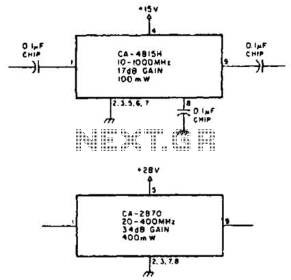
Wideband Power Amplifier Circuit
Using TRW part number CA-815H, a 17 dB gain amplifier capable of delivering 100 mW over a frequency range of 10 to 1000 MHz can be constructed. Additionally, the CA-2870 can provide 0.4 W with a gain of 34 dB...

Signal Generator 20KHz
This function generator IC is specified to work to 20 MHz. So far, this unit works nicely to 50KHz. Since I seldom need signals higher than that, it has taken up a happy home on my workbench and further development...

RF Signal Generator
This signal generator is designed for the realignment of radio receivers. It is an economical and straightforward unit, adequate for its intended application. However, the output is not a pure sine wave, which may limit its suitability for more precise...

Test Signal Generator
This signal generator uses a three channel DAC to generate Composite video signal (CVBS) and S video signal (Y/C separated) at the same time, left one channel is not used in NTSC format. It is assigned for one of the...

Variety of signal generator circuit
The audio function generator integrated circuit ICL8038 is capable of producing square waves, triangle waves, and sine waves. The electrical resistance and potentiometer RP1 are utilized to determine the 8-pin DC potential Ua, which is typically set to 2Ucr/3. A...

Wideband Preamp Circuit
Motorola MWA 110, 120, or 130 are wideband amplifier ICs. This wideband preamp circuit can be used in many applications. Keep the leads short when constructing the circuitry. PC board layout (shading represents copper) and parts layout. X is the...

Signal Generator circuit
The output level was set to 3.8V peak to peak. The initial objective was to compare several different operational amplifiers (op-amps) before further optimizing the circuit. The op-amps evaluated were the TL072, LM4562, and OPA2134. The distortion spectra are presented...