


DTMF FM PLL Receiver
#DTMF
#FM receiver
#PLL synthesizer
#UMA1015
#PIC processor
#LED display
#frequency programming
#audio decoding
#RF communication

Description: This project is a PLL synthesized FM radio which can decode DTMF. The receiving frequency can be set by the PLL circuit from 80-140MHz. The receiver is VERY stable, high sensitivity and easy to build and tune. The FM receiver can decode DTFM signals from a transmitter and present the DTMF data on three LED display. The complete background about this project can be found at my "Wife replace" project. This part is a FM receiver based on a PLL synthesizer UMA1015. The frequency of the PLL synthesizer is programmed by a PIC processor which also control the DTMF circuit and the LED to display information. The Audio output from the FM receiver is connected to a DTMF circuit which is specialised to identify and decode DTMF signals. If there is a valid DTMF tone the PIC will read the data and present it on the LED display. Since I have 3 LED I can display 000 to 999 on the display. More: To the left you will find the preamplifier. It is based on a dualgate fet (You can use almost any dualgate fet). At Gate 1 we have the antenna input. L1 and C1 will tune the antenna for best performance. To find perfect antenna match you can solder the antenna to a tap-point of L1. I can not tell you where to put the tap, you have to experiment yourself (1-2 turns from ground side should be a good place). Gate 2 is biased to give high gain. At drain you will find another tuned circuit L2 and C2. This circuit should also be tuned for best performance. I have chosen L2 to be a transformer slugtuned Inductor. It has an AL value of 7. With 5 turns primary I will get L= n2*AL => 52*7=175nH. This inductor transform the RF to the secondary side 2 turns which is connected to mixer 1. SA615 circuit: In the SA615 you will find an oscillator at pin 3 and 4. This oscillator is connected internally to mixer 1. At pin 4 you can find a coil L3 parallel with a capacitor of 3.9pF. How to make this oscillator voltage controlled? Parallel with the 3.9pF capacitor you will find a varicap diod. The capacitans of this diod is dependent of the voltage over it. So, by applying a voltage to the varicap the internal capacitance will change and so will the resonance frequency. The purpose of the 10pF serie capacitor is to remove the VtuneDC-voltage. By changing the Vtune voltage to the varicap the frequency will slide a few MHz. At pin 3 you will find a resistor Re. This resistor is added to raise the oscillator current. A small portion of the oscillator frequency is probed by a dual gate FET. The FET acts as an amplifier and have a high in impendance. The buffered oscillator signal, then enter the PLL synthesizer at pin 6. In this project I use a bit different PLL synthesizer. The reason I choose this one is because I found 4 of them in some cordless phones I found in a container. Let's have a look at the schematic. A Dualgate FET is used as a buffer from the oscillator. This buffer amplifies the signal and prevent glitches and noise from the PLL to go back into the oscillator. The pin 6 is the input pin for RF signal. The UMA1015 PLL is programmed in serially way and use 3 pins for it (Latch, Clock, Data). I advice you to read the datasheet to find the details about the internal register of this circuit. I did find this circuit easy to use and understand. Pin 18 has a resistor connected to ground. This resistor set the current which the PLL use with the phase comparator and charge pump. In my construction this PLL will lock the PLL to a constant frequency so there is no critical timing to take care of, as it would be if the PLL should jump from one frequency to another. A external crystal module is used as reference frequency. In this construction I use a 12.8MHz module as reference frequency. The PLL has an output to generate the tuning voltage. You can find this output at pin 3. Some capacitor and resistor form a filter and this voltage is then connected back to the varicap at the oscillator. The basic function of the PLL is that the frequency from the oscillator is divided with a programmed ration and compared with the fixed frequency which also is divided with another programmed ration. The phase of the two signals is compared and generate a DC voltage at the PD-output. This DC voltage will regulate the main RF oscillator until the signal in the PLL has the same phase. This will occur when both signals in the PLL has the same phase. The PLL has now locked the RF oscillator to the desired frequency. If you want more detailed information about PLL synthesizer and phase comparators, I suggest you read the zipped document at bottom or search the internet for PLL synthesizer. The mixer 1 mix the RF signal with the oscillator frequency and the IF (Intermediate Frequency) is 455kHz. Two ceramic filters damp all other unwanted frequency and the signal then enter the FM demodulator at pin 14. To demodulate FM the SA615 use a Quad coil. The audio signal can be found at pin 9 and the RSSI signal can be found at pin 7.
The project involves a PLL synthesized FM radio capable of decoding DTMF signals, operating within a frequency range of 80-140 MHz. The system is designed for stability, high sensitivity, and ease of assembly and tuning. The core of the receiver is based on the UMA1015 PLL synthesizer, which is controlled by a PIC processor. This processor manages both the DTMF decoding and the LED display that indicates the decoded DTMF data, allowing for a range of 000 to 999 to be displayed using three LEDs.
The preamplifier stage utilizes a dual-gate FET, with Gate 1 serving as the antenna input. Components L1 and C1 are used to optimize antenna performance. For tuning, the antenna can be connected to a tap-point on L1, with experimentation required to determine the optimal position. Gate 2 is configured for high gain, and a tuned circuit consisting of L2 and C2 is utilized for additional performance enhancement. L2 is a transformer slug-tuned inductor with an AL value of 7, providing a calculated inductance of 175 nH for the RF transformation to the secondary side, which connects to mixer 1.
The SA615 component features an internal oscillator connected to mixer 1, with oscillation controlled by a parallel coil L3 and a capacitor of 3.9 pF at pin 4. A varicap diode is incorporated to allow voltage control of the oscillator's frequency; this diode's capacitance varies with the applied voltage, enabling frequency adjustment. A series capacitor of 10 pF is included to filter out the DC voltage from the tuning signal. A resistor at pin 3 enhances the oscillator current, while a dual-gate FET buffers the oscillator signal before it enters the PLL synthesizer at pin 6.
The UMA1015 PLL synthesizer is programmed serially via three pins (Latch, Clock, Data) and operates with a reference frequency provided by a 12.8 MHz external crystal module. The PLL regulates the oscillator frequency by comparing the phase of the divided oscillator signal with a fixed reference frequency. The output at pin 3 generates a tuning voltage that is filtered before being fed back to the varicap diode. The mixer combines the RF signal with the oscillator frequency, resulting in an intermediate frequency (IF) of 455 kHz. Ceramic filters eliminate unwanted frequencies before the signal reaches the FM demodulator at pin 14, where FM demodulation occurs using a Quad coil. The audio output is accessible at pin 9, and the received signal strength indicator (RSSI) signal can be found at pin 7.This project is a PLL synthesized FM radio which can decode DTMF. The receiving frequency can be set by the PLL circuit from 80-140MHz. The receiver is VERY stable, high sensitivity and easy to build and tune. The FM receiver can decode DTFM signals from a transmitter and present the DTMF data on three LED display. The complete background about this project can be found at my "Wife replace" project. This part is a FM receiver based on a PLL synthesizer UMA1015. The frequency of the PLL synthesizer is programmed by a PIC processor which also control the DTMF circuit and the LED to display information.
The Audio output from the FM receiver is connected to a DTMF circuit which is specialised to identify and decode DTMF signals. If there is a valid DTMF tone the PIC will read the data and present it on the LED display. Since I have 3 LED I can display 000 to 999 on the display. To the left you will find the preamplifier. It is based on a dualgate fet (You can use almost any dualgate fet). At Gate 1 we have the antenna input. L1 and C1 will tune the antenna for best performance. To find perfect antenna match you can solder the antenna to a tap-point of L1. I can not tell you where to put the tap, you have to experiment yourself (1-2 turns from ground side should be a good place). Gate 2 is biased to give high gain. At drain you will find another tuned circuit L2 and C2. This circuit should also be tuned for best performance. I have chosen L2 to be a transformer slugtuned Inductor. It has an AL value of 7. With 5 turns primary I will get L= n2*AL => 52*7=175nH. This inductor transform the RF to the secondary side 2 turns which is connected to mixer 1. SA615 circuit: In the SA615 you will find an oscillator at pin 3 and 4. This oscillator is connected internally to mixer 1. At pin 4 you can find a coil L3 parallel with a capacitor of 3.9pF. How to make this oscillator voltage controlled? Parallel with the 3.9pF capacitor you will find a varicap diod. The capacitans of this diod is dependent of the voltage over it. So, by applying a voltage to the varicap the internal capacitance will change and so will the resonance frequency.
The purpose of the 10pF serie capacitor is to remove the VtuneDC-voltage. By changing the Vtune voltage to the varicap the frequency will slide a few MHz. At pin 3 you will find a resistor Re. This resistor is added to raise the oscillator current. A small portion of the oscillator frequency is probed by a dual gate FET. The FET acts as an amplifier and have a high in impendance. The buffered oscillator signal, then enter the PLL synthesizer at pin 6. In this project I use a bit different PLL synthesizer. The reason I choose this one is because I found 4 of them in some cordless phones I found in a container. Let's have a look at the schematic. A Dualgate FET is used as a buffer from the oscillator. This buffer amplifies the signal and prevent glitches and noise from the PLL to go back into the oscillator.
The pin 6 is the input pin for RF signal. The UMA1015 PLL is programmed in serially way and use 3 pins for it (Latch, Clock, Data). I advice you to read the datasheet to find the details about the internal register of this circuit. I did find this circuit easy to use and understand. Pin 18 has a resistor connected to ground. This resistor set the current which the PLL use with the phase comparator and charge pump. In my construction this PLL will lock the PLL to a constant frequency so there is no critical timing to take care of, as it would be if the PLL should jump from one frequency to another. A external crystal module is used as reference frequency. In this construction I use a 12.8MHz module as reference frequency. The PLL has an output to generate the tuning voltage. You can find this output at pin 3. Some capacitor and resistor form a filter and this voltage is then connected back to the varicap at the oscillator.
The basic function of the PLL is that the frequency from the oscillator is divided with a programmed ration and compared with the fixed frequency which also is divided with another programmed ration. The phase of the two signals is compared and generate a DC voltage at the PD-output. This DC voltage will regulate the main RF oscillator until the signal in the PLL has the same phase. This will occur when both signals in the PLL has the same phase. The PLL has now locked the RF oscillator to the desired frequency. If you want more detailed information about PLL synthesizer and phase comparators, I suggest you read the zipped document at bottom or search the internet for PLL synthesizer.
The mixer 1 mix the RF signal with the oscillator frequency and the IF (Intermediate Frequency) is 455kHz. Two ceramic filters damp all other unwanted frequency and the signal then enter the FM demodulator at pin 14.
To demodulate FM the SA615 use a Quad coil. The audio signal can be found at pin 9 and the RSSI signal can be found at pin 7.
The project involves a PLL synthesized FM radio capable of decoding DTMF signals, operating within a frequency range of 80-140 MHz. The system is designed for stability, high sensitivity, and ease of assembly and tuning. The core of the receiver is based on the UMA1015 PLL synthesizer, which is controlled by a PIC processor. This processor manages both the DTMF decoding and the LED display that indicates the decoded DTMF data, allowing for a range of 000 to 999 to be displayed using three LEDs.
The preamplifier stage utilizes a dual-gate FET, with Gate 1 serving as the antenna input. Components L1 and C1 are used to optimize antenna performance. For tuning, the antenna can be connected to a tap-point on L1, with experimentation required to determine the optimal position. Gate 2 is configured for high gain, and a tuned circuit consisting of L2 and C2 is utilized for additional performance enhancement. L2 is a transformer slug-tuned inductor with an AL value of 7, providing a calculated inductance of 175 nH for the RF transformation to the secondary side, which connects to mixer 1.
The SA615 component features an internal oscillator connected to mixer 1, with oscillation controlled by a parallel coil L3 and a capacitor of 3.9 pF at pin 4. A varicap diode is incorporated to allow voltage control of the oscillator's frequency; this diode's capacitance varies with the applied voltage, enabling frequency adjustment. A series capacitor of 10 pF is included to filter out the DC voltage from the tuning signal. A resistor at pin 3 enhances the oscillator current, while a dual-gate FET buffers the oscillator signal before it enters the PLL synthesizer at pin 6.
The UMA1015 PLL synthesizer is programmed serially via three pins (Latch, Clock, Data) and operates with a reference frequency provided by a 12.8 MHz external crystal module. The PLL regulates the oscillator frequency by comparing the phase of the divided oscillator signal with a fixed reference frequency. The output at pin 3 generates a tuning voltage that is filtered before being fed back to the varicap diode. The mixer combines the RF signal with the oscillator frequency, resulting in an intermediate frequency (IF) of 455 kHz. Ceramic filters eliminate unwanted frequencies before the signal reaches the FM demodulator at pin 14, where FM demodulation occurs using a Quad coil. The audio output is accessible at pin 9, and the received signal strength indicator (RSSI) signal can be found at pin 7.This project is a PLL synthesized FM radio which can decode DTMF. The receiving frequency can be set by the PLL circuit from 80-140MHz. The receiver is VERY stable, high sensitivity and easy to build and tune. The FM receiver can decode DTFM signals from a transmitter and present the DTMF data on three LED display. The complete background about this project can be found at my "Wife replace" project. This part is a FM receiver based on a PLL synthesizer UMA1015. The frequency of the PLL synthesizer is programmed by a PIC processor which also control the DTMF circuit and the LED to display information.
The Audio output from the FM receiver is connected to a DTMF circuit which is specialised to identify and decode DTMF signals. If there is a valid DTMF tone the PIC will read the data and present it on the LED display. Since I have 3 LED I can display 000 to 999 on the display. To the left you will find the preamplifier. It is based on a dualgate fet (You can use almost any dualgate fet). At Gate 1 we have the antenna input. L1 and C1 will tune the antenna for best performance. To find perfect antenna match you can solder the antenna to a tap-point of L1. I can not tell you where to put the tap, you have to experiment yourself (1-2 turns from ground side should be a good place). Gate 2 is biased to give high gain. At drain you will find another tuned circuit L2 and C2. This circuit should also be tuned for best performance. I have chosen L2 to be a transformer slugtuned Inductor. It has an AL value of 7. With 5 turns primary I will get L= n2*AL => 52*7=175nH. This inductor transform the RF to the secondary side 2 turns which is connected to mixer 1. SA615 circuit: In the SA615 you will find an oscillator at pin 3 and 4. This oscillator is connected internally to mixer 1. At pin 4 you can find a coil L3 parallel with a capacitor of 3.9pF. How to make this oscillator voltage controlled? Parallel with the 3.9pF capacitor you will find a varicap diod. The capacitans of this diod is dependent of the voltage over it. So, by applying a voltage to the varicap the internal capacitance will change and so will the resonance frequency.
The purpose of the 10pF serie capacitor is to remove the VtuneDC-voltage. By changing the Vtune voltage to the varicap the frequency will slide a few MHz. At pin 3 you will find a resistor Re. This resistor is added to raise the oscillator current. A small portion of the oscillator frequency is probed by a dual gate FET. The FET acts as an amplifier and have a high in impendance. The buffered oscillator signal, then enter the PLL synthesizer at pin 6. In this project I use a bit different PLL synthesizer. The reason I choose this one is because I found 4 of them in some cordless phones I found in a container. Let's have a look at the schematic. A Dualgate FET is used as a buffer from the oscillator. This buffer amplifies the signal and prevent glitches and noise from the PLL to go back into the oscillator.
The pin 6 is the input pin for RF signal. The UMA1015 PLL is programmed in serially way and use 3 pins for it (Latch, Clock, Data). I advice you to read the datasheet to find the details about the internal register of this circuit. I did find this circuit easy to use and understand. Pin 18 has a resistor connected to ground. This resistor set the current which the PLL use with the phase comparator and charge pump. In my construction this PLL will lock the PLL to a constant frequency so there is no critical timing to take care of, as it would be if the PLL should jump from one frequency to another. A external crystal module is used as reference frequency. In this construction I use a 12.8MHz module as reference frequency. The PLL has an output to generate the tuning voltage. You can find this output at pin 3. Some capacitor and resistor form a filter and this voltage is then connected back to the varicap at the oscillator.
The basic function of the PLL is that the frequency from the oscillator is divided with a programmed ration and compared with the fixed frequency which also is divided with another programmed ration. The phase of the two signals is compared and generate a DC voltage at the PD-output. This DC voltage will regulate the main RF oscillator until the signal in the PLL has the same phase. This will occur when both signals in the PLL has the same phase. The PLL has now locked the RF oscillator to the desired frequency. If you want more detailed information about PLL synthesizer and phase comparators, I suggest you read the zipped document at bottom or search the internet for PLL synthesizer.
The mixer 1 mix the RF signal with the oscillator frequency and the IF (Intermediate Frequency) is 455kHz. Two ceramic filters damp all other unwanted frequency and the signal then enter the FM demodulator at pin 14.
To demodulate FM the SA615 use a Quad coil. The audio signal can be found at pin 9 and the RSSI signal can be found at pin 7.

fm radio receiver
A very simple circuit for an FM receiver that does not require an integrated circuit (IC) and utilizes only a single transistor. The functionality of this transistor is uncertain. This design represents a regenerative or super-regenerative radio receiver. There are...

LED dot display based Battery charge level indicator circuit diagram
In various situations, it is necessary to indicate the amount of battery charge using methods such as LED dot displays or LED bar displays. This circuit utilizes the LM3914 integrated circuit to serve as a battery charge indicator with an...

MT8870D Integrated DTMF Receiver With Enhance Sensitivity
The MT8885 is a monolithic DTMF transceiver equipped with a call progress filter. It is manufactured using CMOS technology, which ensures low power consumption and high reliability. The receiver section is designed based on the industry-standard MT8870 DTMF receiver. The...

CM8870 CMOS Integrated DTMF Receiver
The CAMD CM8888 8888-2 is a fully integrated DTMF transceiver that features adjustable guard time, automatic tone burst mode, call progress mode, and a fully compatible interface for 8051 and 8086/8 microprocessors. It is manufactured using advanced CMOS technology, which...
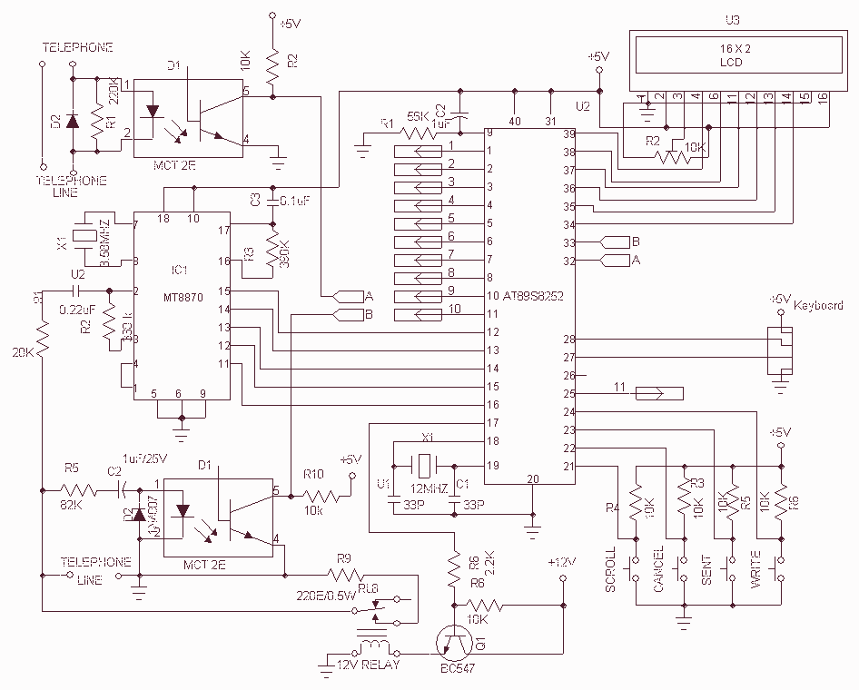
SMS through Telephone with AT89S8252
The main objective of this system is to transmit message or text through ordinary Land Line Telephone from one end (source) to another end (designation). This is achieved by the DTMF technology. It has two sections: one for editing the...

LED Sound level display circuit by using IC LM3915
This is a simple audio sound level LED display circuit diagram. The circuit is entirely based on a single integrated circuit, the LM3915 from National Semiconductor. The LM3915 is a monolithic integrated circuit that displays the audio sound level using...

LED bar peak program meter display for audio
A vertical column of LEDs is configured so that as the audio signal level rises, an increasing number of LEDs illuminate. The LEDs are arranged in increments of 6 dB. The circuit features a fast response time and a one-second...

DTMF COM
The Simple MT 8870 Decoder can be operated using any type of DTMF tones emitted from devices such as landlines, mobile phones, computers, and radio transmitters, including ham radios equipped with DTMF capabilities. This decoder can activate a relay when...

A high-performance FM receiver for audio and digital applicatons
A block diagram and a schematic of the receiver are shown in Figures 2 and 3, respectively. In Figure 3, L6 and L7 are spaced 0.6 inch for a loss of about 0.5 dB. Q4 is the first RF amplifier....