


envelope sampler
#AM demodulator
#AC amplifier
#rectifier
#analog switch
#phase error
#signal voltage
#RF circuit
#demodulation
#envelope detection
#adjustable gain

Description: This is an AM demodulator that remains unaffected by phase errors in the demodulated signal. Phase error is a common issue encountered in simple diode/low pass filter demodulators. The input stage features an adjustable AC amplifier controlled by P1. Rectifiers A1 and A3 charge capacitor C6 with the maximum signal voltage. The analog switches are managed by a clock signal derived from the carrier frequency. Consequently, the sampler can be utilized in various devices such as facsimile machines, radios, and speed processors, as its clock frequency is directly influenced by the received carrier frequency.
The described AM demodulator circuit is designed to effectively handle amplitude modulation signals while minimizing the impact of phase errors, which are prevalent in traditional demodulation methods. The architecture begins with an adjustable AC amplifier, allowing for fine-tuning of the input signal's amplitude, enhancing the overall performance of the demodulator. The potentiometer P1 plays a crucial role in this adjustment, ensuring optimal signal levels for subsequent processing.
Following the amplifier stage, rectifiers A1 and A3 are employed to convert the amplified AC signal into a DC voltage. This rectification process is essential for extracting the envelope of the modulated signal, which contains the original information. Capacitor C6 is charged to the peak voltage of the incoming signal, providing a stable voltage reference for further processing.
The integration of analog switches, controlled by a clock signal derived from the carrier frequency, allows for dynamic sampling of the demodulated signal. This clock signal ensures that the sampling occurs in synchrony with the incoming carrier, thereby mitigating phase errors that could distort the output. The flexibility of this design enables its application in various electronic devices, including facsimile machines, radios, and speed processors, where accurate demodulation is critical.
The system's adaptability to different carrier frequencies makes it particularly valuable in communication systems, where signal integrity is paramount. The ability to directly control the clock frequency based on the received carrier ensures that the demodulator can maintain performance across a range of operating conditions, making it a robust solution for AM demodulation tasks.This is an AM demodulator which is not affected by phase errors in the demodulated signal. Phase error is a type of error commonly found in simple diode/low pass filter demodulators. At the input stage is an AC amplifier which is adjustable through P1. A1 and A3 are the rectifiers that charges C6 with the maximum signal voltage. The analog switche s are controlled by a clock signal. The clock signal is derived from the carrier frequency. In this way the sampler can be applied in different devices like facsimile, radio and speed processors since its clock frequency is directly controlled by the received carrier frequency.
The described AM demodulator circuit is designed to effectively handle amplitude modulation signals while minimizing the impact of phase errors, which are prevalent in traditional demodulation methods. The architecture begins with an adjustable AC amplifier, allowing for fine-tuning of the input signal's amplitude, enhancing the overall performance of the demodulator. The potentiometer P1 plays a crucial role in this adjustment, ensuring optimal signal levels for subsequent processing.
Following the amplifier stage, rectifiers A1 and A3 are employed to convert the amplified AC signal into a DC voltage. This rectification process is essential for extracting the envelope of the modulated signal, which contains the original information. Capacitor C6 is charged to the peak voltage of the incoming signal, providing a stable voltage reference for further processing.
The integration of analog switches, controlled by a clock signal derived from the carrier frequency, allows for dynamic sampling of the demodulated signal. This clock signal ensures that the sampling occurs in synchrony with the incoming carrier, thereby mitigating phase errors that could distort the output. The flexibility of this design enables its application in various electronic devices, including facsimile machines, radios, and speed processors, where accurate demodulation is critical.
The system's adaptability to different carrier frequencies makes it particularly valuable in communication systems, where signal integrity is paramount. The ability to directly control the clock frequency based on the received carrier ensures that the demodulator can maintain performance across a range of operating conditions, making it a robust solution for AM demodulation tasks.This is an AM demodulator which is not affected by phase errors in the demodulated signal. Phase error is a type of error commonly found in simple diode/low pass filter demodulators. At the input stage is an AC amplifier which is adjustable through P1. A1 and A3 are the rectifiers that charges C6 with the maximum signal voltage. The analog switche s are controlled by a clock signal. The clock signal is derived from the carrier frequency. In this way the sampler can be applied in different devices like facsimile, radio and speed processors since its clock frequency is directly controlled by the received carrier frequency.

Adjustable gain amplifier circuit diagram of a test device isolation
An adjustable gain test is conducted in preparation for an isolation amplifier circuit, utilizing the optical coupling isolation amplifier ISO100. This adjustable gain can form part of a test device for the isolation amplifier. The circuit gain can be adjusted...

DZW75-48 50 50II high-frequency rectifier circuit
Alternating positive and negative voltage pulses from the secondary winding of a high-frequency transformer (T) are full-wave rectified by high-frequency switching diodes (V1, V2). The output is then filtered through inductors (L1) and capacitors (C2, C3, C4) which form an...

Zero rectifier regulator schematic
The pre-regulator circuit is connected to a capacitor and a resistor element. The regulator operates in its conducting direction through the input. A capacitor is connected to AC power, and in the blocking direction, it limits the current, allowing the...

Half-wave rectifier
This circuit allows for precise half-wave rectification of the incoming signal. It exhibits a gain of 0 for positive signals and a gain of -1 for negative signals. By reversing the orientation of both diodes, the output polarity can be...

DTL-TTL controlled buffered analog switch
This analog switch utilizes the 2N4860 JFET, which features a low on-resistance of 25 ohms and minimal leakage current. The LM102 is employed as a voltage buffer in the circuit. Additionally, this configuration can be modified for use in a...

Am demodulator
Amplifying and limiting the AM carrier is achieved through the IF gain block, which provides a gain of 55 dB or higher with a limiting level of 40 µV. The limited carrier is then fed to the detector at the...
Zero rectifier regulator schematic
The pre-regulator circuit is connected to a capacitor and a resistor element. The regulator operates in its conducting direction through the input. A capacitor is connected to AC power, and in the blocking direction, it limits the current, allowing the...
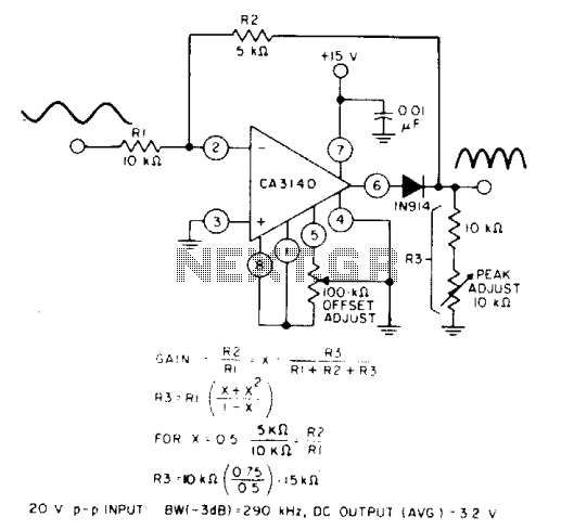
full-wave rectifier
When the equality of two equations is satisfied, the full-wave output of the circuit is symmetrical. The circuit utilizes a CA3140 BiMOS operational amplifier in an inverting gain configuration.
The circuit design featuring the CA3140 BiMOS operational amplifier is characterized by...

Single-phase full-wave rectifier circuit 02 phase
The closed-loop system consists of longitudinal and transverse components. The circuit operates as follows: a control circuit from the stepping motor CNC system issues a command, which the receiver detects. This signal is processed through a phase-sensitive rectifier to convert...