


TV antenna booster

Description: The circuit depicted is a TV antenna booster utilizing the BF180 transistor. It functions within the UHF band and provides a gain of 15 dB. Capacitors C2, C3, C4, and C5, along with inductors L3 and L4, create a UHF band-pass filter. The input signal is directed to the emitter of Q1 via this filter. Resistors R2 and R3 are used to bias the transistor Q1, which is configured in a common base arrangement.
The TV antenna booster circuit employs the BF180 transistor, known for its high-frequency performance, making it suitable for UHF applications. The common base configuration is advantageous in this design as it offers a low input impedance, which is ideal for matching the high-frequency signals typically received by UHF antennas.
The band-pass filter formed by capacitors C2, C3, C4, C5, and inductors L3 and L4 is critical in this circuit. It selectively allows the desired UHF signals to pass while attenuating unwanted frequencies, thus enhancing the overall performance of the antenna system. The gain of 15 dB indicates that the circuit can significantly amplify weak signals, improving the quality of received television broadcasts.
Biasing resistors R2 and R3 ensure that the transistor operates within its optimal range. Proper biasing is essential for maintaining the linearity of the amplifier and preventing distortion of the amplified signal. The circuit's design must also consider power supply decoupling to minimize noise and ensure stable operation under varying load conditions.
Overall, this TV antenna booster circuit is an effective solution for enhancing UHF signal reception, making it a valuable addition to any television setup in areas with weak signal coverage.The circuit shown here is of a TV antenna booster based on the transistor BF180. The circuit operates in the UHF band and has a gain of 15dB. Capacitors C2, C3 C4, C5 and inductors L3, L4 forms a UHF band pass filter. The input signal is fed to the emitter of Q1 through this filter. Resistor R2 and R3 biases the transistor Q1 which is wired in the common base configuration.
The TV antenna booster circuit employs the BF180 transistor, known for its high-frequency performance, making it suitable for UHF applications. The common base configuration is advantageous in this design as it offers a low input impedance, which is ideal for matching the high-frequency signals typically received by UHF antennas.
The band-pass filter formed by capacitors C2, C3, C4, C5, and inductors L3 and L4 is critical in this circuit. It selectively allows the desired UHF signals to pass while attenuating unwanted frequencies, thus enhancing the overall performance of the antenna system. The gain of 15 dB indicates that the circuit can significantly amplify weak signals, improving the quality of received television broadcasts.
Biasing resistors R2 and R3 ensure that the transistor operates within its optimal range. Proper biasing is essential for maintaining the linearity of the amplifier and preventing distortion of the amplified signal. The circuit's design must also consider power supply decoupling to minimize noise and ensure stable operation under varying load conditions.
Overall, this TV antenna booster circuit is an effective solution for enhancing UHF signal reception, making it a valuable addition to any television setup in areas with weak signal coverage.The circuit shown here is of a TV antenna booster based on the transistor BF180. The circuit operates in the UHF band and has a gain of 15dB. Capacitors C2, C3 C4, C5 and inductors L3, L4 forms a UHF band pass filter. The input signal is fed to the emitter of Q1 through this filter. Resistor R2 and R3 biases the transistor Q1 which is wired in the common base configuration.

Antenna Booster for FM AM and SW Receiver
This AM/FM antenna booster circuit amplifies the broadband signal from the antenna. This antenna booster is designed to work for FM, AM, and SW receivers.
The AM/FM antenna booster circuit is an essential component for enhancing radio reception across various...

oscillator mcpos400 plus
This is a UHF oscillator circuit designed to utilize the Mini-Circuits POS-400+ voltage-controlled oscillator chip. By applying a voltage between 0 to 12V on pin 8, it produces a sine wave output ranging from 200MHz to 380MHz on pin 2;...
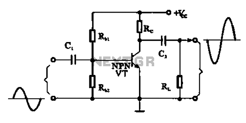
A common emitter amplifier
A common emitter amplifier is a total pole amplification circuit structure featuring a key emitting device. This circuit refers to the emitter of the input signal and the output signal connected to a common ground, forming the basis of fundamental...
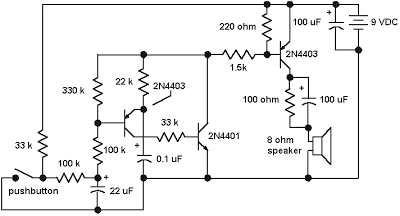
Emergency Siren Simulator
The core of the circuit is a two-transistor flasher, with frequency modulation applied to the base of the first transistor. When the pushbutton is pressed, the oscillation frequency increases to a peak, and upon releasing the button, the frequency decreases...

Simple Transistor Reflex Receivers
This reflex radio project was inspired by Robert Bazian's design. His reflex radio is the "darndest" thing I have seen and his spectacular results inspired me to come up with my own version! These designs are similar to two-transistor circuits...

G STRAIN ENERGY ABSORBER
It is important to know that transistors Q1, Q2, Q3 must not work like an astable (tri-phase) multivibrator (you could verify it on scope (no square waves but NON LINEAR wave between XB, YB, ZB must be displayed on the...

UHF Audio Video Sender Circuit
This audio-video circuit enables wireless audio and visual transmission to a television. The television functions as a receiver, eliminating the necessity for a separate monitor. It can also be connected to a VCR or CCD camera, and can be configured...

XENON STROBE
A two-transistor oscillator generates pulses at approximately 500 Hz to step up the voltage using a 300-mA filament transformer (T1, Radio Shack 273-1384) for charging storage capacitors C2 and C3, which are 250-V electrolytics. At the same time, capacitor C4...

Voice amplifier transistor
Dctl is a two-stage amplifier, with the first stage amplifying the collector voltage of transistor VT1. The second stage, represented by VT2, is proportional to the current flowing through the winding. The RF signal is applied to the sub-base of...