


Remote-sensor-loop-transmitter
#sensor amplifier
#bridge configuration
#voltage to frequency converter
#current loop
#linear output
#integrator
#comparator
#transmitter
#resistance sensor

Description: This circuit features amplifier A1 as a sensor amplifier configured in a bridge arrangement. Amplifiers A2 and A3 are set up as a voltage-to-frequency converter, while A4 functions as the transmitter. The entire sensor/transmitter operates directly from a 4 to 20 mA current loop. The bridge configuration yields a linear output corresponding to variations in the sensor's resistance. The voltage at the output of A1 causes the integrator output of A2 to decrease until it surpasses the comparator threshold voltage of A3. Amplifier A3 activates transistors Q1 and Q2. The output of A2 ramps up at a rate nearly equal to its negative slope, with Q2 providing hysteresis for the comparator. Additionally, Q1 and Q2 mitigate fluctuations in the power supply loop voltage. Amplifier A4 and transistor Q3 are arranged as a constant current sink that activates when the comparator current rises. This increase in loop current transmits the frequency of the voltage-to-frequency converter back to the control circuitry.
The circuit operates on a bridge configuration that enhances sensitivity and linearity in measuring resistance changes from the sensor. The output from amplifier A1 is critical as it translates the resistance variations into a corresponding voltage signal. This voltage is then processed by amplifier A2, which acts as an integrator; its output decreases over time until it reaches a predefined threshold set by amplifier A3, which functions as a comparator. When the output of A2 crosses this threshold, amplifier A3 engages, activating transistors Q1 and Q2.
Transistor Q2 plays a crucial role in providing hysteresis, ensuring that the circuit does not oscillate around the threshold voltage, thus stabilizing the output. Concurrently, Q1 and Q2 help maintain a steady voltage level across the power supply loop, reducing the impact of any voltage variations that could affect the performance of the amplifiers.
Amplifier A4 is designed to operate as a transmitter, while transistor Q3 serves as a constant current sink. When the output from the comparator (A3) increases due to rising current levels, Q3 activates, allowing for the transmission of frequency signals back to the control circuitry. This mechanism enables the system to communicate changes in sensor readings effectively, providing a robust solution for applications requiring precise monitoring of resistance changes in real-time. The overall design ensures that the sensor/transmitter is reliable and efficient, capable of functioning effectively within the specified current loop parameters.This circuit shows amplifier Al as a sensor amplifier in a bridge configuration. Amplifiers A2 and A3 are configured as a voltage to frequency converter and A4 is used as the transmitter. This entire sensor/ transmitter can be powered directly from a 4 to 20 mA current loop. The bridge configuration produces a linear output with respect to the changes in resistance of the sensor.
The voltage at the output of Al causes the integrator output A2 to ramp down until it crosses the comparator threshold voltage of A3. A3 turns on Ql and Q2. Al causes the output of A2 to ramp up at a rate nearly equal to its negative slope, while Q2 provides hysteresis for the comparator. 1n addition, Ql and Q2 help eliminate changes in power supply loop voltage. Amplifier A4 and Q3 are configured as a constant current sink which turns on when the comparator current increases.
The resulting increase in loop current transmits the frequency of the VI F converter back to the control circuitry.
The circuit operates on a bridge configuration that enhances sensitivity and linearity in measuring resistance changes from the sensor. The output from amplifier A1 is critical as it translates the resistance variations into a corresponding voltage signal. This voltage is then processed by amplifier A2, which acts as an integrator; its output decreases over time until it reaches a predefined threshold set by amplifier A3, which functions as a comparator. When the output of A2 crosses this threshold, amplifier A3 engages, activating transistors Q1 and Q2.
Transistor Q2 plays a crucial role in providing hysteresis, ensuring that the circuit does not oscillate around the threshold voltage, thus stabilizing the output. Concurrently, Q1 and Q2 help maintain a steady voltage level across the power supply loop, reducing the impact of any voltage variations that could affect the performance of the amplifiers.
Amplifier A4 is designed to operate as a transmitter, while transistor Q3 serves as a constant current sink. When the output from the comparator (A3) increases due to rising current levels, Q3 activates, allowing for the transmission of frequency signals back to the control circuitry. This mechanism enables the system to communicate changes in sensor readings effectively, providing a robust solution for applications requiring precise monitoring of resistance changes in real-time. The overall design ensures that the sensor/transmitter is reliable and efficient, capable of functioning effectively within the specified current loop parameters.This circuit shows amplifier Al as a sensor amplifier in a bridge configuration. Amplifiers A2 and A3 are configured as a voltage to frequency converter and A4 is used as the transmitter. This entire sensor/ transmitter can be powered directly from a 4 to 20 mA current loop. The bridge configuration produces a linear output with respect to the changes in resistance of the sensor.
The voltage at the output of Al causes the integrator output A2 to ramp down until it crosses the comparator threshold voltage of A3. A3 turns on Ql and Q2. Al causes the output of A2 to ramp up at a rate nearly equal to its negative slope, while Q2 provides hysteresis for the comparator. 1n addition, Ql and Q2 help eliminate changes in power supply loop voltage. Amplifier A4 and Q3 are configured as a constant current sink which turns on when the comparator current increases.
The resulting increase in loop current transmits the frequency of the VI F converter back to the control circuitry.

pippin qrp transmitter
This circuit represents a conventional Colpitts type crystal oscillator, where the output is taken from a low-value collector load resistor. Direct coupling is implemented into the base of a PNP transistor used as an amplifier, resulting in a simplified circuit...

20M Cw Transmitter Circuit
The transmitter features a VXO circuit that drives a keyed amplifier. This keyed amplifier powers an MRF 476 final amplifier, producing approximately 2 watts of output. Additionally, a solid-state T-R switch is incorporated for the receiver. The component values provided...

ATV JR TRANSMITTER 440 MHz
This low-power video transmitter is suitable for remote control applications, surveillance, or amateur radio. It employs seven transistors within a crystal oscillator multiplier RF power amplifier chain, along with a high-level video modulator. A supply voltage ranging from 9 to...

All Transmitter & Receiver schematics
This website was developed to assist students in discovering ideas for their projects or final year projects (FYP). All content presented here is sourced from reliable blogs, websites, and forums. The owner of this website assumes no responsibility for any...
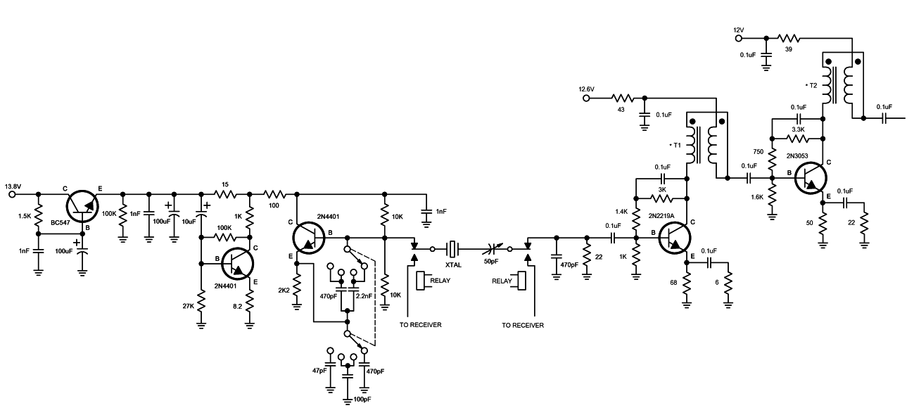
Deluxe Crystal Controlled Transmitter
A high-quality QRP transmitter, named NEXUS 6, is designed to explore issues related to extremely narrow bandwidth communication. This device is not merely a simplified version of a QRP transmitter; it aims to create a cost-effective system that can be...

Command Transmitter-Receiver
The Command Transmitter-Receiver (A3023) is designed to test the command receiver proposed for the Implantable Sensor with Lamp (ISL) in the conceptual design phase. The A3023 consists of two primary components: the Command Transmitter section, which features a 146-MHz (2-m...

50W Tube-Valve SW transmitter
This transmitter operates in the shortwave range from 6 MHz to 22 MHz. Coil L1 serves as the shortwave oscillating coil for the 6SA7 vacuum tube and is commercially available. Capacitor C1 is a variable capacitor with a capacitance range...

Precision QRP Transmitter
This compact transmitter is suitable for less demanding Doppler propagation measurements. It is designed for operation on the 80m band but can be easily adapted for the 40m or 20m bands. The output power is approximately 500mW of unmodulated carrier,...

Projects
This project was inspired by a desire to create something unique rather than with the expectation of it becoming a practical transmitter. At the time of writing, the project is in the breadboarding phase, and a decision has yet to...