


Shutter-speed tester
#solar cell
#FET
#field-effect transistor
#light sensor
#drain current
#gate-source bias
#voltage measurement
#photovoltaic

Description: The solar cell is connected to the input of the field-effect transistor (FET), Q1, allowing it to generate a positive DC voltage at the gate when illuminated by light through the open shutter. This illumination reduces the negative gate-source bias established by the source resistor, resulting in an increase in drain current. Consequently, the drain voltage becomes more negative, leading to a decrease in the base current of Q2. As a result, Q2's collector current diminishes, causing its collector voltage to become more positive. An amplified positive voltage output is observed at the collector, which is applied directly to the oscilloscope's vertical input, producing a waveform that is vertically displaced whenever light strikes the solar cell.
The described circuit operates based on the interaction between a solar cell and a pair of transistors, specifically a field-effect transistor (FET) and a bipolar junction transistor (BJT). The solar cell serves as a light sensor, converting incident light energy into electrical energy. When light strikes the solar cell, it generates a positive DC voltage, which is fed to the gate of the FET (Q1). This voltage effectively reduces the negative bias at the gate-source junction, which is initially established by a source resistor connected to the FET.
As the gate voltage increases, the drain current through the FET also increases due to the enhanced conductivity of the channel formed by the FET. The increase in drain current leads to a more negative voltage at the drain terminal of Q1. This change in voltage influences the operation of the second transistor, Q2, which is configured to respond to variations in the collector current of Q1.
The decrease in the drain voltage of Q1 results in a reduced base current flowing into Q2. Since the base current of Q2 is directly related to its collector current, a reduction in base current leads to a corresponding decrease in collector current. Consequently, the voltage at the collector of Q2 rises due to the reduced current flow, resulting in a more positive collector voltage.
The amplified output at the collector of Q2 is then directed to an oscilloscope's vertical input. This setup allows for real-time visualization of the voltage changes as a waveform on the oscilloscope display. The waveform reflects the intensity of light striking the solar cell; thus, any fluctuations in light levels will cause the waveform to shift vertically. This circuit effectively demonstrates the principles of light-to-voltage conversion and amplification, showcasing the interaction between photovoltaic elements and transistor-based amplification in electronic applications.The solar cell is connected across the input of the FET (field-effect transistor), Ql, so that it will produce positive dc voltage to the gate when activated by light shining through the open shutter, decreasing the negative gate-source bias already established by the source resistor, and causes an increase in drain current. The drain voltage goes more negative which causes a decrease in Q2's base current. Q2's collector current decreases, and its collector voltage becomes more positive. There is an amplified positive-going voltage output at the collector, and it's applied directly to the oscilloscope's vertical input, producing a waveform that is displaced vertically whenever light strikes the cell.
The described circuit operates based on the interaction between a solar cell and a pair of transistors, specifically a field-effect transistor (FET) and a bipolar junction transistor (BJT). The solar cell serves as a light sensor, converting incident light energy into electrical energy. When light strikes the solar cell, it generates a positive DC voltage, which is fed to the gate of the FET (Q1). This voltage effectively reduces the negative bias at the gate-source junction, which is initially established by a source resistor connected to the FET.
As the gate voltage increases, the drain current through the FET also increases due to the enhanced conductivity of the channel formed by the FET. The increase in drain current leads to a more negative voltage at the drain terminal of Q1. This change in voltage influences the operation of the second transistor, Q2, which is configured to respond to variations in the collector current of Q1.
The decrease in the drain voltage of Q1 results in a reduced base current flowing into Q2. Since the base current of Q2 is directly related to its collector current, a reduction in base current leads to a corresponding decrease in collector current. Consequently, the voltage at the collector of Q2 rises due to the reduced current flow, resulting in a more positive collector voltage.
The amplified output at the collector of Q2 is then directed to an oscilloscope's vertical input. This setup allows for real-time visualization of the voltage changes as a waveform on the oscilloscope display. The waveform reflects the intensity of light striking the solar cell; thus, any fluctuations in light levels will cause the waveform to shift vertically. This circuit effectively demonstrates the principles of light-to-voltage conversion and amplification, showcasing the interaction between photovoltaic elements and transistor-based amplification in electronic applications.The solar cell is connected across the input of the FET (field-effect transistor), Ql, so that it will produce positive dc voltage to the gate when activated by light shining through the open shutter, decreasing the negative gate-source bias already established by the source resistor, and causes an increase in drain current. The drain voltage goes more negative which causes a decrease in Q2's base current. Q2's collector current decreases, and its collector voltage becomes more positive. There is an amplified positive-going voltage output at the collector, and it's applied directly to the oscilloscope's vertical input, producing a waveform that is displaced vertically whenever light strikes the cell.
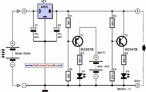
Solar Cell Voltage Regulator
This device is designed to serve as a simple and cost-effective comparator, intended for use in a solar cell power supply system where a quick indication of either too low or acceptable voltage is required. The circuit includes one 5V...

Coulomb meter
Another cause of voltage drift is the input current of IC1, which slowly charges capacitor C1. This effect is particularly noticeable when the output voltage is approximately 0 volts.
The circuit in question involves an integrated circuit (IC1) whose input current...
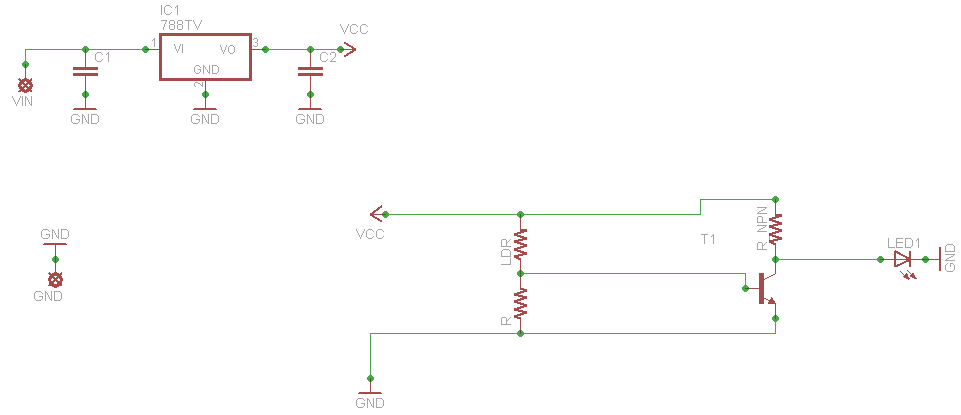
light sensor
When connecting this element in a voltage divider configuration, a high and low signal can be generated based on the amount of light detected by the sensor. An NPN transistor configured as an inverter further filters this signal to produce...

light sensor circuit using pic16c63
This light sensor circuit, utilizing a photosensor, serves as a bridge between light and electronics. It is constructed using an operational amplifier and the PIC16C63 microcontroller to control the sensor. While the circuit is not intended for precision applications, it...

Fet-voltmeter
This FETVM replaces the function of the VTVM and eliminates the need for a standard line cord. Additionally, FET drift rates are significantly better than those of vacuum tube circuits, enabling a full-scale range of 0.5 V, which is not...
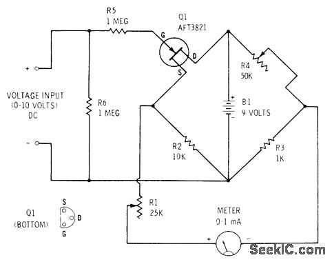
FET VOLTMETER
A Field Effect Transistor (FET) is incorporated into one leg of a Wheatstone bridge, resulting in a meter with an input impedance exceeding 1 megohm. To achieve a zero reading on the meter when no input voltage is present, R4...

EIGHT CHANNEL COMPUTERIZED 3SUP1 SUP SUB2 SUB DIGIT_VM
Displays up to eight different DC voltages on a CRT terminal of a microprocessor under keyboard control, using BASIC commands and a BASIC routine provided in the article. Utilizes a modified Motorola MC14433 dual-lamp integrating analog-to-digital converter. An unknown voltage...

Light Level Droplets Detector
This circuit is a Low-Light Level Drop Detector. It utilizes a self-biasing configuration to detect small changes in light levels.
The Low-Light Level Drop Detector circuit is designed to sense minute variations in ambient light conditions, making it suitable for applications...

FET VOLTMETER
The FETVM serves as a replacement for the VTVM, eliminating the need for a conventional line cord. It features significantly improved drift rates compared to vacuum tube circuits, enabling a full-scale range of 0.5 volts, which is typically unfeasible with...