


Single-supply-wide-range-sync-separator
#sync separator
#video signal
#single supply
#wide range
#peak detector
#comparator
#IC
#buffer
#amplifier

Description: This circuit extracts the synchronization pulses from a video signal across a wide range of amplitudes and operates on a single +15 V supply. IC1 buffers and amplifies the incoming signal and applies it via C3 to the peak detector, which consists of D2 and C4. The signal is also directed to one input of a comparator, IC2. The other input of IC2 is set at a voltage corresponding to approximately 0.065 of the peak video amplitude, using the resistor divider R4/R5. The trigger points of IC2 are positioned near the bottom of the sync pulses to minimize spurious noise. These resistors also provide leakage across C4, necessitating a compromise between excessive ripple and the speed of response to falling signal levels. The output of IC2 swings between 0 and 15 V, making it compatible with CMOS logic levels; however, further buffering is recommended, which is achieved using a CMOS inverter. The maximum input amplitude is limited by the saturation of IC1's output, while the minimum acceptable level is determined by the forward voltage drop of the de-restoring clamp D1, which should be either a germanium or a Schottky diode.
The circuit operates effectively in video signal processing applications by ensuring reliable extraction of sync pulses. The configuration of IC1 as a buffer and amplifier is crucial for maintaining signal integrity, especially in environments with varying input amplitudes. The peak detector formed by D2 and C4 plays a significant role in stabilizing the output by capturing the peak voltage levels, which is essential for accurate sync pulse extraction.
The comparator IC2 is designed to trigger at specific voltage levels that correlate with the sync pulse characteristics, thereby filtering out unwanted noise. The resistor divider R4/R5 is strategically chosen to set the threshold voltage for the comparator, ensuring that it only responds to valid sync pulses while ignoring noise that may appear at lower voltage levels. This design consideration enhances the robustness of the circuit against spurious signals, which is a common challenge in video signal processing.
The output stage of IC2 provides a CMOS-compatible signal, suitable for interfacing with other digital circuits. The recommendation for additional buffering through a CMOS inverter is a prudent design choice, as it enhances the drive capability of the output signal and isolates the comparator from downstream circuits, ensuring that variations in load do not affect the performance of the sync pulse extraction.
Finally, the choice of the de-restoring clamp D1, whether a germanium or Schottky diode, is critical for maintaining the minimum acceptable input signal level. The forward voltage drop characteristics of these diodes are essential for ensuring that the sync pulses are accurately restored and that the overall circuit functions effectively within the specified voltage ranges. This comprehensive approach to circuit design ensures reliable performance across various video signal processing applications.This circuit extracts the sync pulses from a video signal over a wide range of amplitudes and operates a single +15 V supply. IC1 buffers and amplifies the incoming signal and applies it via C3 to the peak detector, consisting of D2 and C4.
It is also applied to one input of a comparator, IC2. The other input of IC2 is set at a voltage corresponding to about 0.065 of the peak video amplitude, by the divider R4/R5. The trigger points of IC2 are set near the bottom of the sync pulses which help prevent spurious noise. These resistors also leak across C4, so they must be chosen as a compromise he tween excessive ripple and speed of response to falling signal levels.
The IC2 output swings between 0 and 15 V and is conveniently CMOS compatible, but further buffering is advisable, hence the CMOS inverter. Maximum input amplitude is set by saturating IC1"s output. The minimum acceptable level is set by the forward voltage drop of the de restoring clamp D1, which should be either a germanium (as shown) or a Schottky diode.
The circuit operates effectively in video signal processing applications by ensuring reliable extraction of sync pulses. The configuration of IC1 as a buffer and amplifier is crucial for maintaining signal integrity, especially in environments with varying input amplitudes. The peak detector formed by D2 and C4 plays a significant role in stabilizing the output by capturing the peak voltage levels, which is essential for accurate sync pulse extraction.
The comparator IC2 is designed to trigger at specific voltage levels that correlate with the sync pulse characteristics, thereby filtering out unwanted noise. The resistor divider R4/R5 is strategically chosen to set the threshold voltage for the comparator, ensuring that it only responds to valid sync pulses while ignoring noise that may appear at lower voltage levels. This design consideration enhances the robustness of the circuit against spurious signals, which is a common challenge in video signal processing.
The output stage of IC2 provides a CMOS-compatible signal, suitable for interfacing with other digital circuits. The recommendation for additional buffering through a CMOS inverter is a prudent design choice, as it enhances the drive capability of the output signal and isolates the comparator from downstream circuits, ensuring that variations in load do not affect the performance of the sync pulse extraction.
Finally, the choice of the de-restoring clamp D1, whether a germanium or Schottky diode, is critical for maintaining the minimum acceptable input signal level. The forward voltage drop characteristics of these diodes are essential for ensuring that the sync pulses are accurately restored and that the overall circuit functions effectively within the specified voltage ranges. This comprehensive approach to circuit design ensures reliable performance across various video signal processing applications.This circuit extracts the sync pulses from a video signal over a wide range of amplitudes and operates a single +15 V supply. IC1 buffers and amplifies the incoming signal and applies it via C3 to the peak detector, consisting of D2 and C4.
It is also applied to one input of a comparator, IC2. The other input of IC2 is set at a voltage corresponding to about 0.065 of the peak video amplitude, by the divider R4/R5. The trigger points of IC2 are set near the bottom of the sync pulses which help prevent spurious noise. These resistors also leak across C4, so they must be chosen as a compromise he tween excessive ripple and speed of response to falling signal levels.
The IC2 output swings between 0 and 15 V and is conveniently CMOS compatible, but further buffering is advisable, hence the CMOS inverter. Maximum input amplitude is set by saturating IC1"s output. The minimum acceptable level is set by the forward voltage drop of the de restoring clamp D1, which should be either a germanium (as shown) or a Schottky diode.

50Ohm driver
To buffer a test generator to the outside world requires an amplifier with sufficient bandwidth and power handling capability. The circuit is a very simple unity gain buffer. It has a fairly high input impedance, a 50-ohm output impedance, a...

Video Operated Relay
Many Video Operated Relay (VOR) circuits have been published in recent years for use in connection with ATV repeater controllers or automatic videotape logging systems. Unfortunately, many of these circuits fail to properly detect certain video signals depending on their...

Amplifiers connecting Bridge
This is a circuit that ensures that you can connect two amplifiers together so you get more power. When called in bridge linking two amplifiers plus you can link the outputs of the amplifiers to the speaker. One of the...
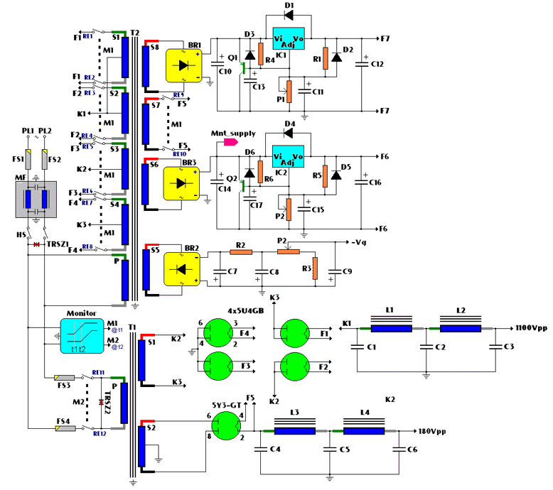
Power Supply For Amplifier
The following circuit illustrates a power supply for an amplifier circuit diagram. Features include ease of construction and adequate electrical response.
The power supply circuit for an amplifier is a crucial component that ensures the amplifier operates effectively. It typically consists...

Video-Out Coupling
To connect a video signal to multiple destinations, a distribution amplifier is required to match the 75-ohm video cable. This amplifier terminates the incoming cable at 75 ohms and provides several outputs, each maintaining a 75-ohm output impedance. Typically, this...
Amplifier Timer
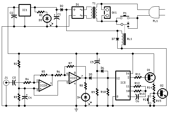
This circuit turns off an amplifier or any other device when a low-level audio signal fed to its input is absent for 15 minutes at least. Pushing P1, the device is switched on, feeding any appliance connected to SK1. Input...

Peak Detector
A 0-to-5 V input drives the negative input of the LM392 comparator if the reset (pin 12) of the DC4060BE is pulled high and then low, causing all outputs of ICF1 to be forced low. This action forces the positive...
%2Busing%2Bop%2Bamp%2B741%2Bic%2B.png "Zero Crossing Detector ZCD Comparator circuit using 741 op amp circuit")
Zero Crossing Detector (ZCD): Comparator circuit using 741 op amp
A zero crossing detector (ZCD) is a voltage comparator that switches its output between +Vsat and -Vsat (where Vsat is the saturation voltage, approximately 14V) when the input crosses the zero reference voltage. Comparators are fundamental operational amplifier circuits that...

Wide-range-peak-detector
IC1 and IC2 form an inverting half-wave precision rectifier and peak detector circuit. Negative input signals that swing with peaks larger than the voltage on C1 cause this capacitor to charge to the new peak voltage. The capacitor retains this...