


Stalled-Output Detector
#stalled-output
#detector
#pulse
#monitoring
#circuit protection
#signal loss
#diagnostic
#feedback
#safety

Description: This circuit can be utilized to detect a stuck output or node in a circuit, or a loss of data or pulses. The pulse train charges capacitor C1 and biases transistor Q1 on, which illuminates the LED. If the input remains high, transistor Q2 turns off the LED.
This circuit functions as a detection mechanism for output states and data integrity in electronic systems. The primary components include a capacitor (C1), two transistors (Q1 and Q2), and an LED indicator.
When a pulse train is applied to the circuit, capacitor C1 begins to charge. This charging process causes transistor Q1 to enter a conducting state, allowing current to flow through the LED, which indicates that the circuit is operational. The illumination of the LED serves as a visual confirmation of a valid signal presence.
If the input signal remains in a high state for an extended period, transistor Q2 becomes activated. The role of Q2 is to monitor the input level, and when it detects that the input does not transition as expected, it turns off the LED. This action signifies that the output may be stuck or that there is a potential loss of data or pulse signals.
The design of this circuit is essential for applications requiring reliable data transmission and output monitoring. It can be particularly useful in digital communication systems, where signal integrity is critical. By incorporating this detection circuit, engineers can ensure that any anomalies in signal behavior are promptly indicated, allowing for timely troubleshooting and maintenance.
Overall, the circuit serves as a crucial tool in maintaining the functionality and reliability of electronic systems, providing both visual feedback and diagnostic capabilities. This circuit can be used to detect a stuck output or node in a circuit, or a loss of data or pulses. The pulse trai n charges CI and biases Ql on, which lights the LED. If the input remains high, Q2 extinguishes the LED.
This circuit functions as a detection mechanism for output states and data integrity in electronic systems. The primary components include a capacitor (C1), two transistors (Q1 and Q2), and an LED indicator.
When a pulse train is applied to the circuit, capacitor C1 begins to charge. This charging process causes transistor Q1 to enter a conducting state, allowing current to flow through the LED, which indicates that the circuit is operational. The illumination of the LED serves as a visual confirmation of a valid signal presence.
If the input signal remains in a high state for an extended period, transistor Q2 becomes activated. The role of Q2 is to monitor the input level, and when it detects that the input does not transition as expected, it turns off the LED. This action signifies that the output may be stuck or that there is a potential loss of data or pulse signals.
The design of this circuit is essential for applications requiring reliable data transmission and output monitoring. It can be particularly useful in digital communication systems, where signal integrity is critical. By incorporating this detection circuit, engineers can ensure that any anomalies in signal behavior are promptly indicated, allowing for timely troubleshooting and maintenance.
Overall, the circuit serves as a crucial tool in maintaining the functionality and reliability of electronic systems, providing both visual feedback and diagnostic capabilities. This circuit can be used to detect a stuck output or node in a circuit, or a loss of data or pulses. The pulse trai n charges CI and biases Ql on, which lights the LED. If the input remains high, Q2 extinguishes the LED.
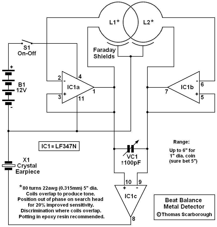
Detector switch circuits
A simple test circuit designed for troubleshooting audio and radio equipment. It can inject a square wave signal rich in harmonics or be used with headphones as an audio tracer. A single-pole double-throw switch is utilized to toggle between injection...

Pulse sequence detector
The resistor divider connected between Q1 and Q2 supplies IH to Q1 after input A triggers it. It also prevents the input from triggering Q2 until Q1 conducts. Consequently, the first input pulse after input A is applied will supply...

Gated pulse descrambler
This circuit includes an amplifier and a video detector along with a secondary subcarrier detector for synchronization recovery. A pulse-former circuit modulates the gain of the main channel, enhancing it during synchronization intervals. Additionally, there is a provision for subcarrier...

Simple Safety Circuit Circuit
The simple two-hand safety control switch consists of two pushbutton switches connected in series; both must be depressed to energize the relay.
The two-hand safety control switch is designed to enhance safety in applications where the operation of machinery or equipment...

Pulse-amplitude-discriminator
A 1-V amplitude pulse activates SCR1, but lacks sufficient amplitude to activate SCR2. A 3-V input pulse is delayed in reaching SCR1 due to the 10-KΩ and 0.001-µF integrating network. Instead, it activates SCR2, subsequently increasing the common emitter voltage...

Detector And Controller
Many applications require analog signals to be sensed and digital signals to be controlled. A way to detect these points is by using a 555 timer in an unconventional configuration. This method will also add hysteresis to the circuit and...

Feedback oscillator
The circuit oscillates because the transistor shifts the phase of the signal 180 degrees from the base to the collector. Each of the RC networks in the circuit is designed to shift the phase 60 degrees at the frequency of...
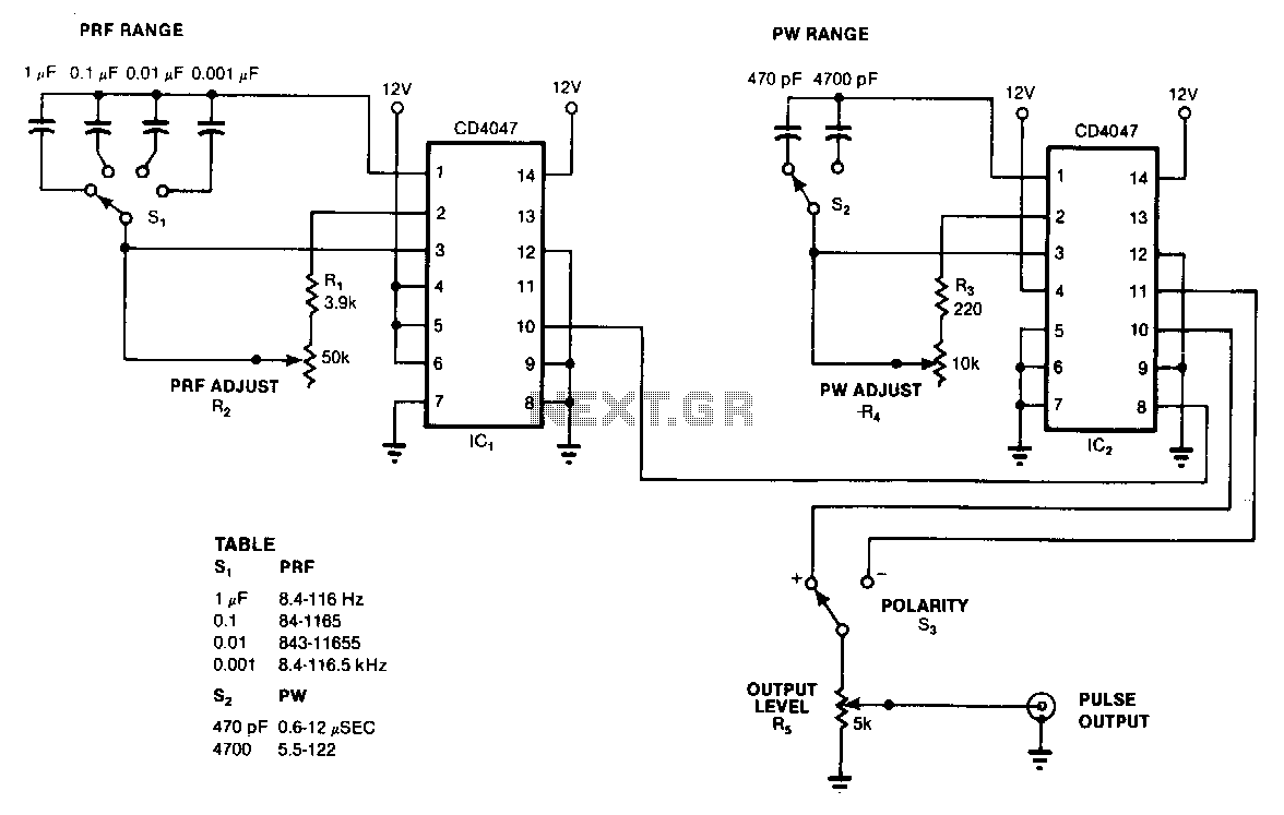
Wide-ranging-pulser
The characteristics of an output pulse depend on the timing components of two multivibrators. The frequency of IC1 in freerunning astable mode determines the pulse repetition frequency (PRF), while the width of the pulse is dictated by the monostable operation...

OCL yourself feedback amplifier analysis
The DC feedback circuit is illustrated in Figure 1-31. In this circuit, resistor R7 is connected to the output terminal, which is the midpoint of the static differential input stage voltage Vr, between the base terminals. This configuration represents a...