


VLQC circuit
#quenching circuit
#transistor
#compact design
#low power
#cross-talk avoidance
#afterpulsing reduction
#detector
#parasitic capacitance
#array
#optical

Description: VLQC is a quenching circuit developed in the laboratory to meet the specific requirements of an array, including high compactness, cross-talk avoidance, and low afterpulsing. In the VLQC design, a single transistor is utilized to perform the sensing, quenching, and reset functions, significantly reducing the overall parasitic capacitance of the detector and consequently lowering system power consumption, as well as minimizing pixel-to-pixel optical coupling and afterpulsing. The accompanying image illustrates a test integrated circuit that incorporates the VLQC. Aside from the output buffer, which is essential for driving pads, the area occupied by the VLQC is comparable to that of a 20µm SPAD.
The VLQC circuit is engineered to optimize performance in applications where space and efficiency are critical. The integration of a single transistor for multiple functions simplifies the design and minimizes the number of components, which contributes to the compactness of the overall system. This arrangement not only enhances the reliability of the circuit by reducing potential points of failure but also allows for easier integration into larger systems.
The quenching process is vital in ensuring that the detector can reset rapidly after a photon detection event, thus enabling it to be ready for the next event without significant downtime. The low afterpulsing characteristic is particularly important in high-speed applications, as it reduces the likelihood of false signals that can arise from residual charge in the detector.
Moreover, the output buffer plays a crucial role by ensuring that the VLQC can effectively interface with external circuits or pads, providing the necessary drive strength to accommodate various load conditions. The compact design of the VLQC, comparable to a 20µm SPAD, allows for high-density arrangements in sensor arrays, making it suitable for applications such as imaging systems, LIDAR, and other optical detection technologies where space and performance are paramount.
In conclusion, the VLQC represents a significant advancement in quenching circuit design, balancing the need for compactness with the operational requirements of modern detection systems. Its innovative use of a single transistor for multiple roles, combined with a design that minimizes parasitic capacitance, positions it as a leading solution in the field of photodetection.VLQC is a quenching circuit designed in our laboratories to perfectly suit the constraints of an array, i. e. high compactness, cross-talk avoidance and low afterpulsing. In VLQC a single transistor performs the sensing, quenching and reset tasks drastically reducing the overall detector parasitic capacitance and thus system power consumption, pixel-to-pixel optical
coupling and afterpulsing. The picture below shows a test integrated circuit comprising the VLQC. A part from the output buffer that is necessary to drive pads, VLQC area is comparable with a 20um SPAD area.
The VLQC circuit is engineered to optimize performance in applications where space and efficiency are critical. The integration of a single transistor for multiple functions simplifies the design and minimizes the number of components, which contributes to the compactness of the overall system. This arrangement not only enhances the reliability of the circuit by reducing potential points of failure but also allows for easier integration into larger systems.
The quenching process is vital in ensuring that the detector can reset rapidly after a photon detection event, thus enabling it to be ready for the next event without significant downtime. The low afterpulsing characteristic is particularly important in high-speed applications, as it reduces the likelihood of false signals that can arise from residual charge in the detector.
Moreover, the output buffer plays a crucial role by ensuring that the VLQC can effectively interface with external circuits or pads, providing the necessary drive strength to accommodate various load conditions. The compact design of the VLQC, comparable to a 20µm SPAD, allows for high-density arrangements in sensor arrays, making it suitable for applications such as imaging systems, LIDAR, and other optical detection technologies where space and performance are paramount.
In conclusion, the VLQC represents a significant advancement in quenching circuit design, balancing the need for compactness with the operational requirements of modern detection systems. Its innovative use of a single transistor for multiple roles, combined with a design that minimizes parasitic capacitance, positions it as a leading solution in the field of photodetection.VLQC is a quenching circuit designed in our laboratories to perfectly suit the constraints of an array, i. e. high compactness, cross-talk avoidance and low afterpulsing. In VLQC a single transistor performs the sensing, quenching and reset tasks drastically reducing the overall detector parasitic capacitance and thus system power consumption, pixel-to-pixel optical
coupling and afterpulsing. The picture below shows a test integrated circuit comprising the VLQC. A part from the output buffer that is necessary to drive pads, VLQC area is comparable with a 20um SPAD area.

Bridge circuit
The transistor is configured as an audio oscillator, utilizing an audio transformer in the collector. The secondary winding is connected to a linear potentiometer. The ratio between the two sections of the potentiometer from the slider is proportional to the...

Phone In Use Electronics Project
Phone In Use Indicator Electronics Project using 5 resistors, 2 NPN transistors, 4 diodes, and 2 light-emitting diodes.
The Phone In Use Indicator is an electronic project designed to visually indicate when a telephone line is active. This circuit employs a...

Two transistor siren
The circuit diagram illustrates a simple two-transistor alarm circuit powered by a 9V PP3 battery. In this configuration, the two transistors are arranged to create an oscillator. The frequency of the oscillator increases when switch S2 is pressed and decreases...

Simple Intercom Circuit Transistor
The circuit diagram represents a simple yet effective intercom system entirely based on transistors. It consists of three stages along with an RC amplifier. When the pushbutton S2 is pressed, the amplifier circuit around transistor T1 is activated.
The intercom circuit...

Low power timer switch
The timing circuit utilizes an electronic switch composed of F1, F2, and VT1 to reduce quiescent current to approximately 1 to 2 A with the 555 timer. Upon initial power-up, the voltage across capacitor C2 cannot instantly change, causing the...
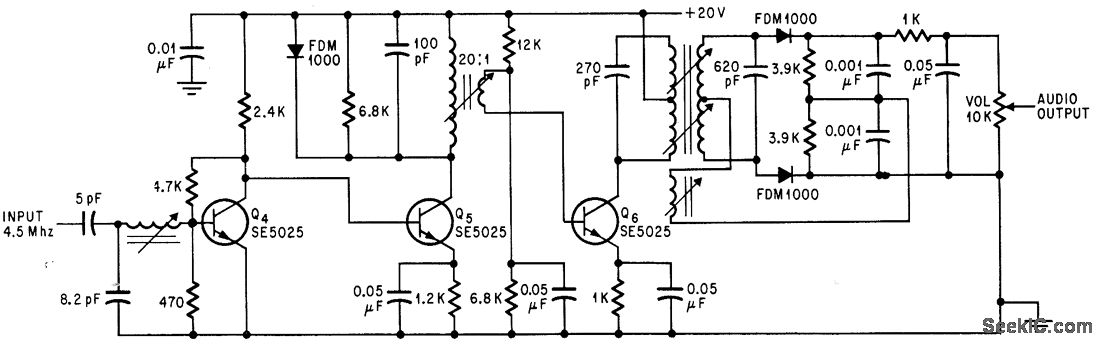
SOUND I F FOR COLOR TV
Utilizes three transistor stages and a Foster-Seeley discriminator to produce an audio output of 1 V peak-to-peak. -D. Bray, Solid State Makes Debut in Big Screen Color TV, Electronics, 39:8, p 99-105.
The circuit in question employs a combination of three...

Low Power Regulator Reference
This is a simple circuit of a low-power voltage regulator reference. This circuit can produce a stable voltage reference.
The low-power voltage regulator reference circuit is designed to provide a consistent output voltage, which is crucial for various electronic applications requiring...

Wilf Rigter`s SIMD1 V2
In the never-ending quest for simplicity, even one extra diode is a price I loathe to pay. To avoid using extra components, it struck me that the two diodes in SIMD1 V1 were connected like the two junctions in one...
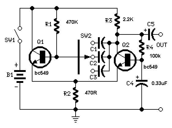
Simple Square wave Generator using transistors ~ Easy Electronics
A useful feature of this circuit is that the frequency can be changed by modifying the capacitor value. A switch can be added to select between various frequencies.
This circuit utilizes a capacitor in conjunction with an oscillator to determine its...