


IRF9540N Gate Charge Test Circuit Schematic and Datasheet
#IRF9540N
#gate charge
#MOSFET
#switching time
#rectifier
#on resistance
#test circuit
#datasheet
#waveforms
#unclamped

Description: The IRF9540N Gate Charge Test Circuit is illustrated in the diagram below. The IRF9540N is recognized as a rectifier device that employs advanced processing techniques to attain an exceptionally low on-resistance per unit area, as stated in the datasheet. In addition to the Gate Charge Test Circuit Schematic, the IRF9540 datasheet also includes information on the Switching Time Test Circuit and Waveforms, Unclamped Inductive Test Circuit, and Peak Diode Recovery dv/dt Test Circuit.
The IRF9540N Gate Charge Test Circuit is designed to evaluate the gate charge characteristics of the IRF9540N MOSFET. This circuit typically consists of a power supply, a resistor to limit the gate current, and measurement equipment to capture the gate charge waveforms. The gate charge, denoted as Qg, is critical for understanding the switching performance of the MOSFET, as it influences the turn-on and turn-off times.
The circuit operates by applying a voltage to the gate of the IRF9540N while monitoring the current through the gate resistor. The charge accumulated on the gate capacitance can be determined by integrating the gate current over time. The results provide insights into the efficiency of the MOSFET in various applications, particularly in high-frequency switching scenarios.
Furthermore, the datasheet's inclusion of the Switching Time Test Circuit and associated waveforms allows for a comprehensive analysis of the IRF9540N's performance in dynamic conditions. The Unclamped Inductive Test Circuit evaluates the device's response to inductive loads, while the Peak Diode Recovery dv/dt Test Circuit assesses the recovery characteristics of the body diode under high dv/dt conditions. Collectively, these tests provide a thorough understanding of the IRF9540N's operational limits and suitability for specific applications in power electronics.IRF9540N Gate Charge Test Circuitis schemed in the diagram below. IRF9540N is known to be rectifier device with advanced processing techniques to achieve extremely low on resistance per silicon area, according to the datasheet. Other thanGate Charge Test Circuit Schematic, you will find such Switching Time Test Circuit and Waveforms, Unclamped Ind
uctive Test Circuit, and Peak Diode Recovery dv/dt Test Circuit in the depth of the IRF9540 datasheet.
The IRF9540N Gate Charge Test Circuit is designed to evaluate the gate charge characteristics of the IRF9540N MOSFET. This circuit typically consists of a power supply, a resistor to limit the gate current, and measurement equipment to capture the gate charge waveforms. The gate charge, denoted as Qg, is critical for understanding the switching performance of the MOSFET, as it influences the turn-on and turn-off times.
The circuit operates by applying a voltage to the gate of the IRF9540N while monitoring the current through the gate resistor. The charge accumulated on the gate capacitance can be determined by integrating the gate current over time. The results provide insights into the efficiency of the MOSFET in various applications, particularly in high-frequency switching scenarios.
Furthermore, the datasheet's inclusion of the Switching Time Test Circuit and associated waveforms allows for a comprehensive analysis of the IRF9540N's performance in dynamic conditions. The Unclamped Inductive Test Circuit evaluates the device's response to inductive loads, while the Peak Diode Recovery dv/dt Test Circuit assesses the recovery characteristics of the body diode under high dv/dt conditions. Collectively, these tests provide a thorough understanding of the IRF9540N's operational limits and suitability for specific applications in power electronics.IRF9540N Gate Charge Test Circuitis schemed in the diagram below. IRF9540N is known to be rectifier device with advanced processing techniques to achieve extremely low on resistance per silicon area, according to the datasheet. Other thanGate Charge Test Circuit Schematic, you will find such Switching Time Test Circuit and Waveforms, Unclamped Ind
uctive Test Circuit, and Peak Diode Recovery dv/dt Test Circuit in the depth of the IRF9540 datasheet.

Linear Light Dimmer by Power Mosfet
Changing the value of R2 alters the intensity of the lamp in this circuit, demonstrating the utility of a MOSFET as a variable resistor. An N-Channel Power MOSFET, designated as Q1, is utilized in the circuit. The specific part number...

Mosfet circuit schematics
Two working examples have been assembled, one utilizing a PNP and an NPN transistor, and the other employing two MOSFETs. Both circuits function correctly, but as anticipated, the MOSFET circuit draws significantly less current (0.1 mA compared to 4.5 mA)....

Full Wave Rectifier Circuit with Averaging Filter
This circuit is an RMS-calibrated AC voltmeter that provides average readings. Removing capacitor C2 eliminates the averaging function, resulting in a precision full-wave rectifier, while removing capacitor C1 transforms the circuit into an absolute value generator. The operation of the...

Single-phase rectifier DC welding power load from road circuit
A single-phase rectifier DC welding power load from the road circuit is presented. The contactor KM utilizes a CJ20-40A model rated for 220V. An adjustment potentiometer RP is employed to ensure proper arcing, while the relay KA2 is designed for...

MOSFET based step-up joule thief circuit
It employs a low threshold MOSFET and two coupled coils to function as a joule thief. An additional MOSFET is utilized for regulation.
The circuit operates as a joule thief, which is a type of DC-DC converter designed to extract energy...

300 watt 1200 watt MOSFET Amplifier for professionals only
When an amplifier with high watt power is required, this circuit is most suitable for applications such as concerts, theaters, and festivals.
This high-power amplifier circuit is designed to deliver significant output power, making it ideal for large-scale audio applications where...
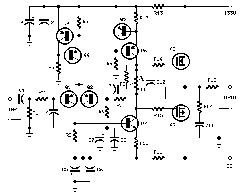
25 Watt MosFet Amplifier
High Quality simple design No need for a preamplifier Can be directly connected to CD players, tuners and tape recorders. Simply add a 10K Log potentiometer (dual gang for stereo) and a switch to cope with the various sources you...

MOSFET Toggle Relay
This circuit is similar to the one above, but uses a N channel mosfet such as IRF530, 540, 640, etc. in place of the NPN transistor. Smaller mosfets could be used, but I don't know the part numbers. I tested...

Bridge Rectifier
This bridge circuit is designed for applications requiring two unequal supply voltages. The lower voltage is obtained using a transformer with symmetric windings and half-wave rectification of the potential across one winding. The higher voltage is derived from the potential...