


Zero volt switching circuit diagrams
#zero volt switching
#AC voltage
#trigger pulse
#555 timer
#comparator
#zero crossing
#circuit diagram
#power electronics

Description: The zero volt switching circuit generates a trigger pulse at the zero crossing of the AC voltage. To facilitate this, the zero crossing of the 555 limit comparator is connected to a single form, with the comparison voltage set by adjusting the static bias voltage at terminal 5 to between 0.7V and 1V. This voltage serves as a reference for a light-emitting diode (LED) device, indicating its presence. A waveform diagram illustrating the working process is provided below. To clarify the concept, a triangle wave is depicted alongside a sine wave, although this does not affect the analysis. Given the low reference voltage, the trigger level is close to zero volts, resulting in a narrower pulse width. Consequently, the SCR switches the AC mains voltage on and off at zero crossings, minimizing the impact of high-frequency radiation interference from adjacent appliances.
The zero volt switching circuit is designed to enhance the efficiency of AC voltage control by utilizing the principle of zero crossing detection. This method is pivotal in reducing electromagnetic interference (EMI) associated with switching operations in electronic circuits. The circuit employs a 555 timer configured as a comparator, which detects the zero crossing point of the AC waveform. By setting the static bias voltage at terminal 5 to a specific range (0.7V to 1V), the circuit establishes a reference voltage that is crucial for triggering the SCR (Silicon Controlled Rectifier) at the precise moment when the AC voltage crosses zero.
In practice, the circuit's operation begins with the AC voltage waveform approaching zero volts. As the waveform crosses this threshold, the 555 timer outputs a pulse that triggers the SCR, allowing current to flow and power to be delivered to the load. This switching action occurs at the zero crossing point, which is beneficial for reducing the generation of electrical noise and minimizing the stress on the connected components. The SCR remains in the conducting state until the current through it falls below a certain threshold, at which point it turns off, effectively stopping the flow of AC voltage to the load.
The waveform diagram referenced in the description illustrates the relationship between the AC voltage, the trigger pulse generated by the 555 timer, and the resultant SCR switching action. The use of a triangle wave in the diagram serves to simplify the visualization of the zero crossing detection process, facilitating a clearer understanding of the timing relationships involved. This method of operation is particularly advantageous in applications where minimizing EMI is critical, such as in sensitive electronic devices and communication equipment.
Overall, the zero volt switching circuit represents a practical solution for effective AC voltage control while maintaining compliance with electromagnetic compatibility standards, thus ensuring reliable operation in various electronic applications. As shown, the zero volt switching circuit in the zero crossing of the AC voltage generated trigger pulse. In order to trigger the zero crossing of the 555 limit comparator conn ected into a single form, the comparison voltage point by setting the corresponding static bias voltage control terminal 5 feet 0.7 ~ 1V, as a comparison with a LED device. It can be used as a reference voltage indicating the presence of a light-emitting. Working Process waveform diagram shown in Figure (b) below. Here, in order to illustrate the problem, it will be drawn into a triangle wave sine wave, but does not affect the analysis process.
Since the reference voltage is relatively low, therefore, the trigger level near zero volts to produce a pulse width narrower. Thus, SCR zero crossing of the AC mains voltage switched on and off, can weaken the impact of high-frequency radiation interference and adjacent appliances.
The zero volt switching circuit is designed to enhance the efficiency of AC voltage control by utilizing the principle of zero crossing detection. This method is pivotal in reducing electromagnetic interference (EMI) associated with switching operations in electronic circuits. The circuit employs a 555 timer configured as a comparator, which detects the zero crossing point of the AC waveform. By setting the static bias voltage at terminal 5 to a specific range (0.7V to 1V), the circuit establishes a reference voltage that is crucial for triggering the SCR (Silicon Controlled Rectifier) at the precise moment when the AC voltage crosses zero.
In practice, the circuit's operation begins with the AC voltage waveform approaching zero volts. As the waveform crosses this threshold, the 555 timer outputs a pulse that triggers the SCR, allowing current to flow and power to be delivered to the load. This switching action occurs at the zero crossing point, which is beneficial for reducing the generation of electrical noise and minimizing the stress on the connected components. The SCR remains in the conducting state until the current through it falls below a certain threshold, at which point it turns off, effectively stopping the flow of AC voltage to the load.
The waveform diagram referenced in the description illustrates the relationship between the AC voltage, the trigger pulse generated by the 555 timer, and the resultant SCR switching action. The use of a triangle wave in the diagram serves to simplify the visualization of the zero crossing detection process, facilitating a clearer understanding of the timing relationships involved. This method of operation is particularly advantageous in applications where minimizing EMI is critical, such as in sensitive electronic devices and communication equipment.
Overall, the zero volt switching circuit represents a practical solution for effective AC voltage control while maintaining compliance with electromagnetic compatibility standards, thus ensuring reliable operation in various electronic applications. As shown, the zero volt switching circuit in the zero crossing of the AC voltage generated trigger pulse. In order to trigger the zero crossing of the 555 limit comparator conn ected into a single form, the comparison voltage point by setting the corresponding static bias voltage control terminal 5 feet 0.7 ~ 1V, as a comparison with a LED device. It can be used as a reference voltage indicating the presence of a light-emitting. Working Process waveform diagram shown in Figure (b) below. Here, in order to illustrate the problem, it will be drawn into a triangle wave sine wave, but does not affect the analysis process.
Since the reference voltage is relatively low, therefore, the trigger level near zero volts to produce a pulse width narrower. Thus, SCR zero crossing of the AC mains voltage switched on and off, can weaken the impact of high-frequency radiation interference and adjacent appliances.

Simple 555 Timer Monostable Circuit
The two circuits below illustrate using the 555 timer to close a relay for a predetermined amount of time by pressing a momentary N/O push button. The circuit on the left can be used for long time periods where the...

555 monostable pulse width modulator
In the 555 datasheet, there is a pulse width modulation circuit that resembles this one, with the only difference being that pin 5 is labeled as 'audio'.
The 555 timer IC is a versatile device commonly used in various applications, including...

555 simple electronic keyboard circuit (2)
Figure 14-41 illustrates a multivibrator circuit utilizing a 555 timer alongside various capacitive and resistive components. The oscillation frequency is determined by the values of Ra, R16, and C3, following the formula f = 1.44 / ((Ra + 2R16) *...
Monoflop practical circuit
Primarily utilized for single-shot timing, shaping, and delay applications. This is achieved through a monostable trigger circuit using the 555 integrated circuit.
The 555 timer IC is a versatile component widely employed in various electronic applications, particularly in generating precise timing...

555 lights remind
The circuit is designed to provide a reminder for lights using a monostable delay configuration. It comprises a monostable delay circuit, a driving circuit, a buzzer, light-emitting diodes (LEDs), and other components. The output signal from the delay circuit, which...
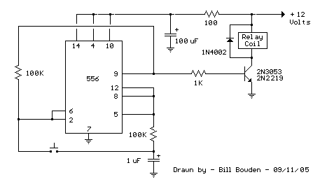
Relay Toggle with 556 schematic
This toggle circuit operates by using a couple 555 timers wired as inverters. Pins 2 and 6 are the threshold and trigger inputs to the first timer and pin 5 is the output. The output at pin 5 will always...

Automobile-ignition
The ignition substitute provides a constant power source for the ignition coil. Its frequency, 0.5-1.0 kHz, is that used by an 8-cylinder engine with an idling speed of 650 RPM, and the unit provides a rapid spark at a 17%...

555 Timer IC For IR Detector Circuit
The circuit illustrates the use of a 555 Timer IC in an infrared (IR) detector configuration. It features a duty cycle of 0.8 milliseconds, a frequency of 120 Hz, and a peak current of 300 mA.
The 555 Timer IC is...

Traffic Lights For Model Cars Or Model Railways
Children today often possess a wide array of toys available in stores. For those with a son or grandson who has a collection of toy cars, a handmade gift such as a set of traffic lights would be greatly appreciated....