


The bilateral band modem circuit composed of NE561B
#NE561B
#modem
#AM modulation
#phase detection
#VCO
#PLL
#bilateral band
#multiplier
#frequency
#signal processing

Description: The figure illustrates a bilateral band modem circuit utilizing the NE561B component. The input modulating signal operates at a loading frequency of f0 = 1 MHz. When the AM modulation signal is applied to the input terminal of the multiplier, it is simultaneously routed to the phase detection circuit through components Rv1, CY1, Y2, and CY2, which establishes the VCO frequency of the PLL at f0.
The bilateral band modem circuit featuring the NE561B is designed to facilitate efficient modulation and demodulation of signals. The NE561B is a versatile integrated circuit widely used in communication systems for its ability to perform analog multiplication and phase detection.
In this specific configuration, the input modulating signal at a frequency of 1 MHz is critical for the operation of the circuit. The amplitude modulation (AM) signal, when fed into the multiplier, is essential for generating the desired output modulation. The phase detection circuit, which includes resistive and capacitive elements (Rv1, CY1, Y2, and CY2), plays a crucial role in maintaining synchronization between the modulated signal and the voltage-controlled oscillator (VCO) frequency of the phase-locked loop (PLL).
The phase detection circuit ensures that any phase discrepancies between the input signal and the VCO output are corrected, thereby stabilizing the frequency output at f0. The use of capacitors and resistors in this configuration helps filter and shape the signals, ensuring that only the desired frequency components are processed.
Overall, this circuit design exemplifies a robust approach to signal modulation, leveraging the NE561B's capabilities to achieve effective communication in various electronic applications. The careful selection of components and their arrangement within the circuit is vital for optimal performance and reliability in real-world scenarios.In the figure is the bilateral band modem circuit composed of NE561B. The loading frequency of the input modulating signal is f0=1MHz. When the AM modulation signal is added on the input terminal of the multiplier, it is also added on the phase detection circuit by Rv1, CY1, Y2 and CY2, and it sets the VCO frequency of PLL at f0..
The bilateral band modem circuit featuring the NE561B is designed to facilitate efficient modulation and demodulation of signals. The NE561B is a versatile integrated circuit widely used in communication systems for its ability to perform analog multiplication and phase detection.
In this specific configuration, the input modulating signal at a frequency of 1 MHz is critical for the operation of the circuit. The amplitude modulation (AM) signal, when fed into the multiplier, is essential for generating the desired output modulation. The phase detection circuit, which includes resistive and capacitive elements (Rv1, CY1, Y2, and CY2), plays a crucial role in maintaining synchronization between the modulated signal and the voltage-controlled oscillator (VCO) frequency of the phase-locked loop (PLL).
The phase detection circuit ensures that any phase discrepancies between the input signal and the VCO output are corrected, thereby stabilizing the frequency output at f0. The use of capacitors and resistors in this configuration helps filter and shape the signals, ensuring that only the desired frequency components are processed.
Overall, this circuit design exemplifies a robust approach to signal modulation, leveraging the NE561B's capabilities to achieve effective communication in various electronic applications. The careful selection of components and their arrangement within the circuit is vital for optimal performance and reliability in real-world scenarios.In the figure is the bilateral band modem circuit composed of NE561B. The loading frequency of the input modulating signal is f0=1MHz. When the AM modulation signal is added on the input terminal of the multiplier, it is also added on the phase detection circuit by Rv1, CY1, Y2 and CY2, and it sets the VCO frequency of PLL at f0..
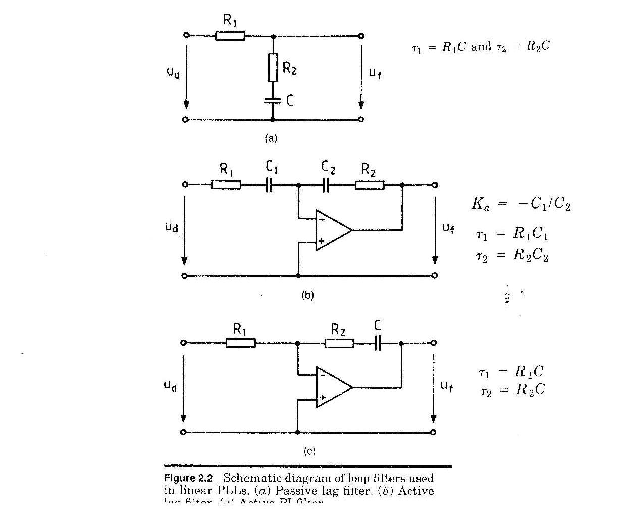
PLL systems
The phase-locked loop (PLL) is a crucial component in maintaining order in various electronic systems. For instance, in an analog television set, a PLL ensures that the image remains stable, keeping the heads at the top of the screen and...

AM base circuit
The circuit is designed for small-signal amplitude modulation (AM). Component C functions as a high-frequency bypass capacitor. Transformers T1 and T2 serve as high-frequency transformers, while the LC resonant circuit operates at the carrier frequency with a passband of 2Fr....

Electronic mosquito repeller circuit diagram
The circuit operates on the principle that insects, such as mosquitoes, can be repelled using sound frequencies in the ultrasonic range (above 20 kHz). It utilizes a Phase-Locked Loop (PLL) integrated circuit, specifically the CMOS 4047, configured as an oscillator...

pll fm demodulator
This circuit is a Phase-Locked Loop (PLL) system designed to function as an FM demodulator. The output of the Voltage-Controlled Oscillator (VCO) tracks the FM signal, and since the input voltage of the VCO is proportional to its output frequency,...

PLL SINGLE TONE DECODER
This circuit can be utilized for Touch-Tone decoding as well as for telephone line and wireless control applications using a single audio frequency. The operating center frequency is determined by components H1 and C1. The resistor R1 should be within...

Internal modem schematics
This diagram illustrates the interaction between an internal SoftV92 Data Fax Modem and a phone line. The modem is manufactured by Zoltrix, although a Conexant utility identifies it as a "Churchill Data Modem." This schematic may be beneficial for repairing...
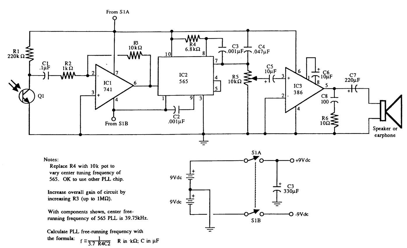
PLL IR LASER LIGHT RECEIVER
Circuit schematics for the 555-based PLL laser light PFM receiver. Although R4 is shown as a resistor, it is advisable to replace it with a 10-kΩ precision potentiometer to allow for fine-tuning of the transmitter's center frequency. Experimentation with the...

Using PLL Phase Locked Loop IC frequency N 1 to 10 of the multiplier circuit
The CMOS IC 4046 Phase-Locked Loop (PLL) operates with a maximum frequency of 1 MHz. It is connected to a programmable divider, allowing it to process input frequencies. As the frequency increases by a factor of t, the circuit's functionality...

VCO Seiler 80Mhz-300Mhz
The voltage-controlled oscillator (VCO) is widely utilized in various RF projects, with a particular emphasis on wideband GHz VCOs over VHF/UHF VCOs. This document outlines a Manhattan Island Pad construction for a VHF VCO, operating from low frequencies of 88...