


Automatic-shutoff
#automatic shutoff
#transistor
#capacitor
#load control
#timer circuit
#delay circuit
#power management
#bias control

Description: When switch S1 is pressed, capacitor C1 begins to charge to the supply voltage. This action creates a forward bias on the gate of transistor Q1, turning it on and allowing current to flow to the load resistor RL. As the charge on capacitor C1 dissipates, the transistor turns off, interrupting the current supply to the load. The load can be a variety of devices, such as a transistor radio or a child's toy. Transistor Q1 is rated for 0.5 A at 60 V DC. With a supply voltage of 9 V DC and capacitor C1 rated at 0.22 µF, a delay of approximately one minute is produced; using a capacitor rated at 10 µF results in a delay of about one hour.
The circuit operates as a simple timing mechanism utilizing a capacitor and a transistor switch. When switch S1 is engaged, the capacitor C1 charges through the supply voltage, which is set at 9 V DC. The charging process allows the voltage across C1 to rise, eventually exceeding the threshold voltage necessary to forward-bias the gate of transistor Q1. This action activates Q1, enabling it to conduct and supply current to the load resistor RL.
The load resistor RL is critical as it determines the current flowing through the connected load, which can be any device that operates within the specifications of the circuit. The choice of transistor Q1 is essential, as it must handle the load current without exceeding its maximum ratings. With a maximum current rating of 0.5 A and a voltage rating of 60 V DC, Q1 is suitable for low-power applications.
As the capacitor C1 discharges through the load when Q1 is activated, it gradually loses its stored charge. Once the voltage across C1 drops below the necessary threshold to keep Q1 in the 'on' state, the transistor will turn off, ceasing current flow to the load. The timing of this process is primarily influenced by the capacitance value of C1. A capacitor rated at 0.22 µF provides a delay of approximately one minute, while a larger capacitor, rated at 10 µF, extends the delay to about one hour. This characteristic allows for flexibility in designing circuits that require specific timing intervals based on the application needs.
Overall, this circuit exemplifies a straightforward approach to creating a timed control mechanism using basic electronic components, with applications ranging from simple toys to more complex electronic devices.When Sl is depressed, Cl begins to charge to the supply voltage. That places a forward bias on the gate of Ql turning it on and supplying current to load resistor RL. When the charge on Clleaks off, the transistor shuts off, cutting off current to the load. That load could be anything from a transistor radio to a child"s toy. Transistor Ql, is rated at 0.5 A at 60 V de. With a supply voltage of 9 V de and with Cl rated at 0.22 J
Related Circuits
The circuit operates as a simple timing mechanism utilizing a capacitor and a transistor switch. When switch S1 is engaged, the capacitor C1 charges through the supply voltage, which is set at 9 V DC. The charging process allows the voltage across C1 to rise, eventually exceeding the threshold voltage necessary to forward-bias the gate of transistor Q1. This action activates Q1, enabling it to conduct and supply current to the load resistor RL.
The load resistor RL is critical as it determines the current flowing through the connected load, which can be any device that operates within the specifications of the circuit. The choice of transistor Q1 is essential, as it must handle the load current without exceeding its maximum ratings. With a maximum current rating of 0.5 A and a voltage rating of 60 V DC, Q1 is suitable for low-power applications.
As the capacitor C1 discharges through the load when Q1 is activated, it gradually loses its stored charge. Once the voltage across C1 drops below the necessary threshold to keep Q1 in the 'on' state, the transistor will turn off, ceasing current flow to the load. The timing of this process is primarily influenced by the capacitance value of C1. A capacitor rated at 0.22 µF provides a delay of approximately one minute, while a larger capacitor, rated at 10 µF, extends the delay to about one hour. This characteristic allows for flexibility in designing circuits that require specific timing intervals based on the application needs.
Overall, this circuit exemplifies a straightforward approach to creating a timed control mechanism using basic electronic components, with applications ranging from simple toys to more complex electronic devices.When Sl is depressed, Cl begins to charge to the supply voltage. That places a forward bias on the gate of Ql turning it on and supplying current to load resistor RL. When the charge on Clleaks off, the transistor shuts off, cutting off current to the load. That load could be anything from a transistor radio to a child"s toy. Transistor Ql, is rated at 0.5 A at 60 V de. With a supply voltage of 9 V de and with Cl rated at 0.22 J
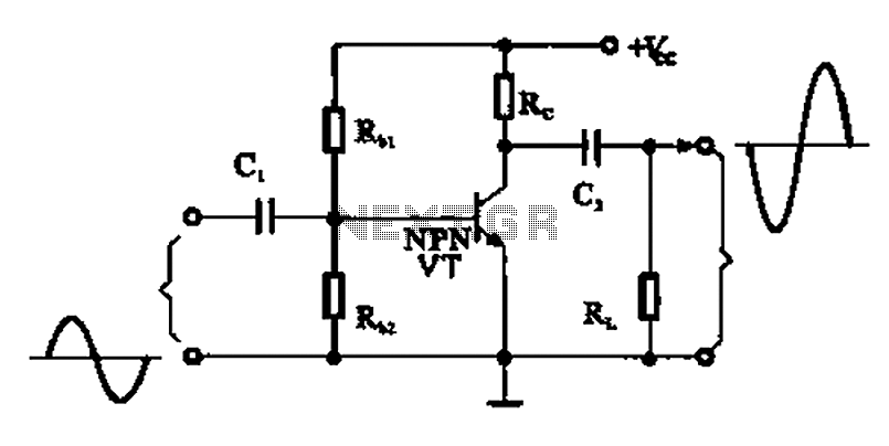
A common emitter amplifier
A common emitter amplifier is a total pole amplification circuit structure featuring a key emitting device. This circuit refers to the emitter of the input signal and the output signal connected to a common ground, forming the basis of fundamental...

12v 10 minute Off-Delay timer
An Xbox 360 console previously experienced a problem known as the 3 Red Lights of Death (3RLOD). To address this issue, the stock heatsinks were removed, and a Koolance external water cooling system was installed. This modification has effectively resolved...

Long-Duration Time Delay
Transistor Q1 and resistors R1, R2, and R3 form a constant current source, with the charge current adjustable to as low as a few nanoamperes. This current is insufficient to activate the UJT, where IP is 0.2 A, unless a...

Transistor Circuit Analysis
The schematic represents a relatively simple transistor circuit. Analyzing such schematics evokes memories of college days spent studying electrical engineering. However, the complexity of the schematic can be daunting after a long time away from the subject. To refresh knowledge,...

audio tone control with 2 transistor
The first BC109C transistor functions as a buffer, offering the circuit an input impedance of approximately 250,000 ohms and a voltage gain just below unity. As the Baxandall tone control circuit is a passive design, it attenuates all audio frequencies....

Basic reference bias circuit transistor - negative voltage feedback
Basic reference bias circuit using a transistor with negative voltage feedback.
The basic reference bias circuit utilizing a transistor with negative voltage feedback is designed to provide a stable output voltage or current that is largely independent of variations in temperature...
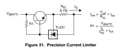
Capacitor Charging Circuit
This Korean SuperCap OEM supports usage in series configurations. Consider whether the implementation will be manual or automatic, such as with a smart battery charger or a power fail backup circuit. It is essential to balance the voltage and provide...

2 channel audio mixer circuit using transistors
This two-channel audio mixer utilizes 2N3904 transistors to create two preamplifiers. The first preamplifier is designed for high gain, suitable for microphone input, while the second preamplifier allows for control over the audio level input. The audio mixer requires a...

1 Transistor Toggle Relay schematic
The circuit below requires a double pole, double throw relay in conjunction with a single transistor to allow toggling the relay with a momentary push button. One set of relay contacts is used to control the load, while the other...