


schematic delay
#delay line
#TDA4661
#baseband
#colour-difference signal
#decoder
#integrated circuit
#signal processing
#video processing

Description: The TDA4661 is an integrated baseband delay line circuit featuring a single line delay. It is designed for use in decoders that produce color-difference signal outputs (R-Y) and (B-Y).
The TDA4661 operates by delaying the baseband signal, which is essential in various video processing applications, particularly in the context of color decoding. The integrated circuit provides a precise delay to the color-difference signals, which helps in synchronizing the chrominance information with the luminance signal in video systems. This synchronization is crucial for maintaining the integrity of the color information during signal processing and transmission.
The circuit typically includes input and output pins for the R-Y and B-Y signals, allowing for straightforward integration into existing decoder architectures. The delay line is implemented using a combination of resistors and capacitors, ensuring that the delay is both stable and adjustable, depending on the specific application requirements.
In practical applications, the TDA4661 can be utilized in television receivers, video monitors, and other devices that require accurate color reproduction. It is important to consider the power supply requirements and the operating temperature range of the TDA4661 to ensure optimal performance in various environments. Proper layout and grounding techniques should also be employed to minimize noise and interference, which can affect the quality of the delayed signals.The TDA4661 is an integrated baseband delay line circuit with one line delay. It is suitable for decoders with colour-difference signal outputs (R-Y) and (B-Y)
The TDA4661 operates by delaying the baseband signal, which is essential in various video processing applications, particularly in the context of color decoding. The integrated circuit provides a precise delay to the color-difference signals, which helps in synchronizing the chrominance information with the luminance signal in video systems. This synchronization is crucial for maintaining the integrity of the color information during signal processing and transmission.
The circuit typically includes input and output pins for the R-Y and B-Y signals, allowing for straightforward integration into existing decoder architectures. The delay line is implemented using a combination of resistors and capacitors, ensuring that the delay is both stable and adjustable, depending on the specific application requirements.
In practical applications, the TDA4661 can be utilized in television receivers, video monitors, and other devices that require accurate color reproduction. It is important to consider the power supply requirements and the operating temperature range of the TDA4661 to ensure optimal performance in various environments. Proper layout and grounding techniques should also be employed to minimize noise and interference, which can affect the quality of the delayed signals.The TDA4661 is an integrated baseband delay line circuit with one line delay. It is suitable for decoders with colour-difference signal outputs (R-Y) and (B-Y)

Video Digitizer Project
This is the original Circuit Cellar ImageWise Transmitter that was initially used. The code was disassembled to capture two half-size images, allowing for the extraction of images from both the odd and even fields. Code was then written to subtract...

Low-Cost Audio Delay Line Uses 1-Bit ADC
Author Jim Walker describes a very low-cost analog delay line circuit using components such as the LM311 comparator and 74HC74 D flip-flop.
The analog delay line circuit presented by Jim Walker utilizes the LM311 comparator and the 74HC74 D flip-flop to...

A practical MS Decoder Circuit
The schematic diagram of the MS Decoder may appear complex, but it is relatively straightforward. Initially, both the Mid and Side signals are buffered using unity gain inverting buffers, which are constructed around IC1b and IC2b. This buffering serves two...
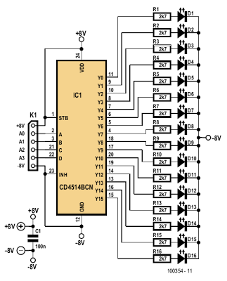
Simple Indicator for Dynamic Limiter Schematic Diagram
The indicator described here is specifically designed for adjusting the dynamic limiter outlined elsewhere in this edition and checking if the maximum level of the reference voltage (P1) requires modification. A 4-to-16 decoder integrated circuit (IC) of type 4514 is...

Background music decoder
This circuit is a background music (SCA) decoder designed to process an input demodulated (multiplex) FM signal. The NE565, a Phase Locked Loop (PLL) integrated circuit, serves as the foundation for this design.
The background music (SCA) decoder circuit utilizes the...

Sca background music decoder
A resistive voltage divider is utilized to establish a bias voltage for the input (pins 2 and 3). The demodulated FM signal is introduced to the input through a two-stage high-pass filter, which serves to provide capacitive coupling and to...

decoder
There is a version without SMD, referred to as version 2.1, which is slightly larger (80 x 100 mm) and features dual drivers capable of handling a 1A load. It operates using the same software. The input voltage from the...

decoder circuit
The PPI-8255 is a general-purpose I/O programmable interface that is typically connected directly to a computer bus. This article demonstrates that the card can serve dual purposes: as an expander port and for direct I/O functionality. The card can be...

low power universal demultiplexer decoder
This circuit functions as a universal decoder, capable of operating either as a dual 1-of-4 decoder or as a single 1-of-8 decoder, depending on the signal applied to the Mode Control (M) input. In the dual mode, each section features...