


Simple Deadband Generator Targets Push-Pull Drivers
#push-pull driver
#npn-pnp transistor
#square-wave signal
#cross conduction
#driver circuit
#inverter
#turn-on characteristics
#turn-off characteristics
#transistor pair
#deadband generator

Description: In typical push-pull driver applications, the NPN-PNP transistor pair is alternately activated and deactivated using a square-wave signal. A basic driver circuit employs an inverter between the V1 and V2 inputs to toggle the output transistors. However, mismatched turn-on and turn-off characteristics of the output transistors can lead to cross conduction during transition periods. This results in high current surges being drawn from the power supply. A simple circuit can be implemented to introduce a desired amount of deadband time between the V1 and V2 control pulses. This circuit utilizes a Schmitt-trigger inverter IC, the 74HC14. With the inclusion of diodes, different time delays can be achieved for the rising and falling edges of the drive waveform. The deadband is determined by the RC time constant. The associated waveforms are self-explanatory. This circuit allows for the use of any type of transistors in the push-pull configuration, reducing the need for matched transistors, which can be costly and effort-intensive to obtain.
In a typical push-pull driver configuration, the NPN and PNP transistors function as complementary devices to drive a load. The operation is controlled via square-wave signals applied to the bases of the transistors, enabling efficient switching. The challenge arises from the inherent differences in the turn-on and turn-off characteristics of the transistors, which can result in simultaneous conduction, known as cross conduction, during the transition phase. This phenomenon can lead to excessive current draw from the power supply, potentially damaging components and reducing overall efficiency.
To mitigate this issue, a circuit can be designed to introduce a deadband between the control signals V1 and V2. By incorporating a Schmitt-trigger inverter, such as the 74HC14, the circuit can provide hysteresis, which enhances noise immunity and provides clean transitions. The use of diodes allows for the adjustment of timing delays for both the rising and falling edges of the output waveform. The deadband duration is primarily influenced by the RC time constant, which can be tailored to suit specific application requirements.
The waveform characteristics, as depicted in the accompanying figures, illustrate the effectiveness of the deadband in preventing cross conduction. The flexibility of this circuit design permits the use of various transistor types in the push-pull arrangement, thus eliminating the need for closely matched pairs. This not only simplifies the design process but also reduces costs associated with sourcing matched transistors, making the circuit more accessible for various applications in electronics.In typical push-pull driver applications, the npn-pnp transistor pair is alternately turned on and off using a square-wave signal. A simple driver circuit uses an inverter between the V1 and V2 inputs to toggle the output transistors.
However, mismatched turn-on and turn-off characteristics of the output transistors can cause cross conduction during the transition periods ( Fig. 1 ). This results in high current surges being drawn from the power supply. The simple circuit shown in Figure 2 can be used to introduce any desired amount of deadband time between V1 and V2 control pulses. The circuit employs a Schmitt-trigger inverter IC, the 74HC14. With the diodes, different time delays can be obtained for the rising and falling edges of the drive waveform.
The deadband is determined by the RC time constant. The waveforms in Figure 3 are self-explanatory. Using this circuit, any type of transistors can be utilized for the push-pull circuit, eliminating the effort and expense required to obtain matched transistors.
In a typical push-pull driver configuration, the NPN and PNP transistors function as complementary devices to drive a load. The operation is controlled via square-wave signals applied to the bases of the transistors, enabling efficient switching. The challenge arises from the inherent differences in the turn-on and turn-off characteristics of the transistors, which can result in simultaneous conduction, known as cross conduction, during the transition phase. This phenomenon can lead to excessive current draw from the power supply, potentially damaging components and reducing overall efficiency.
To mitigate this issue, a circuit can be designed to introduce a deadband between the control signals V1 and V2. By incorporating a Schmitt-trigger inverter, such as the 74HC14, the circuit can provide hysteresis, which enhances noise immunity and provides clean transitions. The use of diodes allows for the adjustment of timing delays for both the rising and falling edges of the output waveform. The deadband duration is primarily influenced by the RC time constant, which can be tailored to suit specific application requirements.
The waveform characteristics, as depicted in the accompanying figures, illustrate the effectiveness of the deadband in preventing cross conduction. The flexibility of this circuit design permits the use of various transistor types in the push-pull arrangement, thus eliminating the need for closely matched pairs. This not only simplifies the design process but also reduces costs associated with sourcing matched transistors, making the circuit more accessible for various applications in electronics.In typical push-pull driver applications, the npn-pnp transistor pair is alternately turned on and off using a square-wave signal. A simple driver circuit uses an inverter between the V1 and V2 inputs to toggle the output transistors.
However, mismatched turn-on and turn-off characteristics of the output transistors can cause cross conduction during the transition periods ( Fig. 1 ). This results in high current surges being drawn from the power supply. The simple circuit shown in Figure 2 can be used to introduce any desired amount of deadband time between V1 and V2 control pulses. The circuit employs a Schmitt-trigger inverter IC, the 74HC14. With the diodes, different time delays can be obtained for the rising and falling edges of the drive waveform.
The deadband is determined by the RC time constant. The waveforms in Figure 3 are self-explanatory. Using this circuit, any type of transistors can be utilized for the push-pull circuit, eliminating the effort and expense required to obtain matched transistors.

Inverter Circuit
This straightforward design of an inverter circuit is capable of delivering high output power with an efficiency of approximately 75%. It provides guidance on constructing an inverter that can meet most power requirements at a reasonable cost. The article outlines...

Inverter Cicuit DIY
This CFL lighting kit is offered by the reputable brand Alfa, recognized for its circuits in inverter-like applications. The kit provides a stable circuit suitable for lighting a PL of 9 watts, 11 watts, or a CFL of up to...

100W Inverter Circuit
This is a 100 Watt inverter circuit designed with a minimal number of components. The circuit utilizes the CD4047 integrated circuit from Texas Instruments to generate 100 Hz pulses, and it employs four 2N3055 transistors to drive the load. The...

Two inverter controlled synchronous motor of the second circuit
Adjust the potentiometers RPi and RPz to modify the speed of two motors.
The circuit utilizes two potentiometers, designated as RPi and RPz, to control the speed of two separate motors. Each potentiometer is connected in a voltage divider configuration, enabling...

500 watt inverter 12vdc to 220vac
The step-up section of this inverter circuit utilizes a transformer with a 12V center-tapped (CT) secondary and a primary winding designed for 0 to 220V. The operating frequency is established by a flip-flop configured to 50 Hz.
The inverter circuit described...
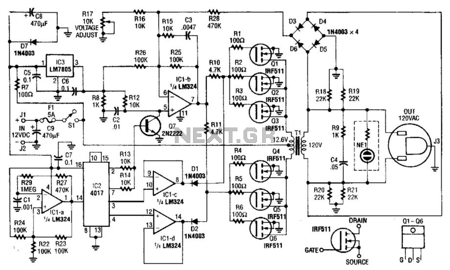
40W 120Vac Inverter
This inverter employs a 12.6-V to 120-V transformer to generate a quasi-sine wave that matches the rms and peak voltage of a pure sine wave. Components Q1 to Q6 require heatsinking, and a 1.5" x 4" aluminum heatsink was utilized...

100w inverter
A 100 Watt inverter circuit utilizing a minimal number of components. It is challenging to construct a reliable inverter with even fewer components. This design employs the CD 4047 integrated circuit from Texas Instruments to generate 100 Hz pulses, along...

Inverter 12V DC to 240V DC circuit diagram
This inverter circuit is designed to power electric razors, stroboscopes, flash tubes, and small fluorescent lamps using a 12-volt car battery. Unlike typical feedback oscillator inverters, this design features a separate oscillator from the output stage, allowing for easy frequency...

inverter
This inverter is designed to power appliances such as televisions and stereos while traveling or camping. It converts 12 VDC (volts direct current) to 120 VAC (volts alternating current).
This inverter functions by utilizing a series of electronic components to transform...