26LS31
26LS31 Quad Differential Line Driver
Overview
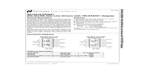
The DS26LS31 is a high-performance quad differential line driver designed for digital data transmission over balanced lines. It features TRI-STATE® outputs and logically ANDed complementary outputs, making it ideal for applications requiring robust noise immunity and high-speed data transfer. The device is fully compatible with LS logic families, with all inputs presenting only one unit load to the driving circuitry.
This component is particularly suited for point-to-point and multi-drop bus communication systems, providing excellent signal integrity in electrically noisy environments. Its differential output configuration minimizes electromagnetic interference (EMI) while maximizing common-mode noise rejection.
Key Features
- Quad differential line driver with complementary outputs
- TRI-STATE outputs for bus-oriented applications
- LS-compatible inputs with single unit loading
- High output current capability: ±20mA typical
- Wide common-mode voltage range: ±7V
- Propagation delay: 15ns typical
- Designed for balanced transmission lines
- Power supply range: 4.5V to 5.5V
- Low power consumption: 85mW typical
- Industrial temperature range: -40°C to +85°C
Applications
The 26LS31 is widely used in various digital communication systems where reliable data transmission is critical:
- RS-422 and RS-485 communication interfaces
- Industrial control systems
- Telecommunications equipment
- Computer peripherals and networking hardware
- Instrumentation and measurement systems
- Automotive electronics
- Medical equipment
- Point-of-sale terminals
- Building automation systems
Electrical Characteristics
Absolute Maximum Ratings
- Supply Voltage (Vcc): 7V
- Input Voltage: 7V
- Output Voltage: ±7V
- Output Short-Circuit Duration: Continuous
- Operating Temperature Range: -40°C to +85°C
- Storage Temperature Range: -65°C to +150°C
Recommended Operating Conditions
- Supply Voltage (Vcc): 4.5V to 5.5V
- Operating Temperature: -40°C to +85°C
- Input High Voltage (VIH): 2V min
- Input Low Voltage (VIL): 0.8V max
- Output Current (High): -20mA
- Output Current (Low): 20mA
DC Electrical Characteristics
- Input High Current (IIH): 20μA max at VIN = 2.7V
- Input Low Current (IIL): -0.4mA max at VIN = 0.4V
- Output High Voltage (VOH): 2.5V min at IOH = -20mA
- Output Low Voltage (VOL): 0.4V max at IOL = 20mA
- Supply Current (ICC): 17mA max (all channels active)
AC Electrical Characteristics
- Propagation Delay (tPLH, tPHL): 15ns typical, 25ns max
- Output Rise/Fall Time: 5ns typical, 10ns max
- Enable Time (tPZH, tPZL): 25ns max
- Disable Time (tPHZ, tPLZ): 25ns max
- Skew Time (tSKEW): 5ns max between complementary outputs
Package Information
The 26LS31 is available in several industry-standard packages:
- 16-pin Plastic Dual In-line Package (PDIP)
- 16-pin Small Outline Integrated Circuit (SOIC)
- 16-pin Shrink Small Outline Package (SSOP)
- 16-pin Thin Shrink Small Outline Package (TSSOP)
Pin Configuration
The device features the following pinout configuration:
- Pin 1: Output Y1 (Channel 1)
- Pin 2: Output Z1 (Channel 1 complement)
- Pin 3: Input A1 (Channel 1 input)
- Pin 4: Input B1 (Channel 1 enable)
- Pin 5: Input A2 (Channel 2 input)
- Pin 6: Input B2 (Channel 2 enable)
- Pin 7: Output Y2 (Channel 2)
- Pin 8: Output Z2 (Channel 2 complement)
- Pin 9: Ground
- Pin 10: Output Y3 (Channel 3)
- Pin 11: Output Z3 (Channel 3 complement)
- Pin 12: Input A3 (Channel 3 input)
- Pin 13: Input B3 (Channel 3 enable)
- Pin 14: Input A4 (Channel 4 input)
- Pin 15: Input B4 (Channel 4 enable)
- Pin 16: VCC (Power supply)
Functional Description
The 26LS31 contains four independent differential line drivers. Each channel consists of an input buffer, a TRI-STATE control gate, and a differential output stage. The outputs are designed to drive balanced transmission lines with controlled impedance.
When the enable input (B) is high, the corresponding driver outputs follow the input state (A), with Y being the non-inverted output and Z being the inverted output. When the enable input is low, both outputs enter a high-impedance state, allowing multiple devices to share a common bus.
Design Considerations
Termination
For optimal performance in point-to-point applications, the transmission line should be terminated at the receiver end with a resistor equal to the characteristic impedance of the line (typically 100Ω for RS-422/485 systems).
Power Supply Decoupling
A 0.1μF ceramic capacitor should be placed as close as possible to the VCC pin to minimize power supply noise and ensure stable operation.
PCB Layout
To maintain signal integrity:
- Keep differential pairs closely coupled
- Maintain consistent trace impedance
- Minimize trace length differences between complementary outputs
- Provide adequate ground plane
Reliability and Quality
The 26LS31 is manufactured using high-reliability processes and undergoes rigorous quality testing, including:
- 100% electrical testing at elevated temperatures
- Burn-in screening (available as an option)
- ESD protection exceeding 2000V (Human Body Model)
- Latch-up immunity testing
Ordering Information
The device is available in various package options with different temperature ranges. Consult the manufacturer's latest datasheet for current ordering codes and packaging options.