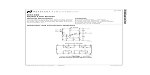
DS3691
DS3691 Low Power Schottky TTL Line Driver
Overview
The DS1691A/DS3691 are low power Schottky TTL line drivers designed to meet the requirements of EIA standards RS-422 and RS-423. These integrated circuits feature four buffered outputs with high source and sink current capability, along with internal short circuit protection for enhanced reliability. The devices offer flexible operation modes through a mode control input, allowing them to function either as four single-ended line drivers or two differential line drivers.
A key feature of the DS3691 is its rise time control capability, enabled through an external capacitor connection. This allows for precise control of signal transition times, particularly useful for suppressing near-end crosstalk in cable applications. The rise time capacitors are primarily intended for waveshaping output signals in single-ended driver mode, though their use in differential mode with waveshaping capacitors requires careful consideration.
Features
- Compliant with EIA standards RS-422 and RS-423
- Flexible operation modes:
- Dual RS-422 line driver when mode pin is low
- Quad RS-423 line driver when mode pin is high
- Four buffered outputs with high current capability
- Internal short circuit protection
- Rise time control via external capacitor
- Low power Schottky TTL technology
- High source and sink current capability
- Designed for waveshaping output signals in single-ended mode
- Operational in both single-ended and differential configurations
Applications
The DS3691 is designed for a wide range of applications in data communication systems:
- RS-422/RS-423 compliant communication interfaces
- Point-to-point and multipoint data transmission systems
- Industrial control systems requiring robust communication
- Telecommunication equipment
- Computer peripheral interfaces
- Networking equipment
- Data acquisition systems
- Instrumentation and measurement systems
Electrical Characteristics
Absolute Maximum Ratings
- Supply Voltage (Vcc): +7V
- Input Voltage: -0.5V to +7V
- Output Short Circuit Duration: Continuous
- Operating Temperature Range: -40°C to +85°C
- Storage Temperature Range: -65°C to +150°C
Recommended Operating Conditions
- Supply Voltage (Vcc): +4.75V to +5.25V
- High-Level Input Voltage: 2.0V min
- Low-Level Input Voltage: 0.8V max
- Operating Free-Air Temperature: -40°C to +85°C
DC Electrical Characteristics
- High-Level Output Voltage (RS-423 mode): 3.5V min at -20mA
- Low-Level Output Voltage (RS-423 mode): 0.4V max at 20mA
- High-Level Output Voltage (RS-422 mode): 2.0V min (differential)
- Low-Level Output Voltage (RS-422 mode): 0.4V max (differential)
- Input Clamp Voltage: -1.5V max at -18mA
- Supply Current (all drivers disabled): 20mA max
- Short-Circuit Output Current: -150mA to +150mA
AC Electrical Characteristics
- Propagation Delay Time (low-to-high): 15ns max
- Propagation Delay Time (high-to-low): 15ns max
- Transition Time (with external capacitor): Adjustable via capacitor value
- Skew Time (differential mode): 5ns max
Package Information
The DS3691 is available in multiple package options to suit different application requirements:
16-Pin Plastic Dual In-Line Package (PDIP)
- Package Code: N
- Dimensions: 19.30mm x 6.35mm
- Lead Pitch: 2.54mm
- Operating Temperature: -40°C to +85°C
16-Pin Small Outline Package (SOIC)
- Package Code: D
- Dimensions: 9.90mm x 3.90mm
- Lead Pitch: 1.27mm
- Operating Temperature: -40°C to +85°C
16-Pin Ceramic Dual In-Line Package (CDIP)
- Package Code: J
- Dimensions: 21.34mm x 7.62mm
- Lead Pitch: 2.54mm
- Operating Temperature: -55°C to +125°C
Functional Description
The DS3691 operates as either four single-ended drivers or two differential drivers based on the state of the mode control pin. When the mode pin is set high, the device functions as four independent RS-423 compatible single-ended drivers. When the mode pin is set low, the device operates as two RS-422 compatible differential drivers.
The rise time control feature allows for adjustment of output signal transition times through an external capacitor connected to the rise time control pin. This feature is particularly valuable in reducing electromagnetic interference (EMI) and minimizing crosstalk in cable applications. The capacitor value directly affects the output signal's rise and fall times, with larger values resulting in slower transitions.
Design Considerations
Mode Selection
The mode pin (typically pin 1) determines the operational configuration of the device. A logic high (>2.0V) selects quad single-ended RS-423 mode, while a logic low (<0.8V) selects dual differential RS-422 mode.
Termination
For RS-422 differential operation, proper termination at the receiver end is critical for signal integrity. A 100Ω termination resistor between the differential pair is typically recommended. For RS-423 single-ended operation, termination should match the cable characteristic impedance.
Power Supply Decoupling
A 0.1μF ceramic capacitor should be placed as close as possible to the Vcc pin to minimize power supply noise and ensure stable operation.
Thermal Management
While the device includes short-circuit protection, prolonged operation at high currents may require thermal considerations. Ensure adequate airflow or heat sinking if operating near maximum ratings.