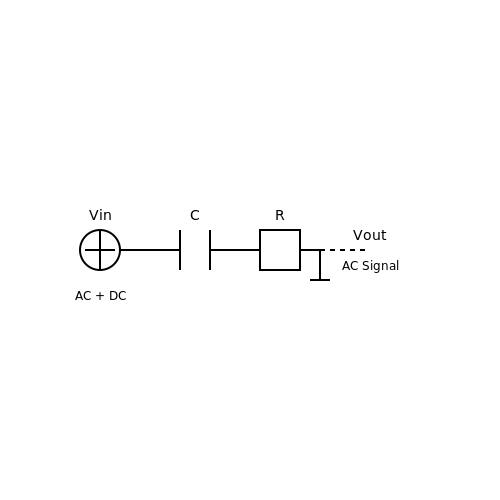
ADC – Basics
1. Definition and Purpose of ADC
1.1 Definition and Purpose of ADC
The Analog-to-Digital Converter (ADC) serves as a crucial interface between the analog world of signals and the digital realm of data processing. Essentially, an ADC transforms continuous signals—such as voltage, sound, or light intensity—into a discrete numerical format that can be utilized by digital systems like microcontrollers or DSPs (Digital Signal Processors). This transformative process is essential for applications ranging from audio recording to scientific measurements in physics and engineering.
At its core, the primary purpose of an ADC is to facilitate the interpretation of analog signals in a digital context. Without ADCs, digital devices would struggle to process real-world data, which is inherently analog. This function is pivotal not only in consumer electronics—such as smartphones and cameras—but also in more sophisticated systems used in research and industry, including sensors in automation and robotics.
Understanding the Operation of ADCs
To grasp how ADCs function, it is important to consider several key parameters: sampling rate, resolution, and quantization error. These parameters collectively determine how accurately and effectively an analog signal can be represented in digital format.
- Sampling Rate: This refers to how frequently the ADC samples the analog signal. It is measured in samples per second (SPS) and is critical for capturing the dynamics of the signal. According to the Nyquist-Shannon sampling theorem, the sampling frequency must be at least twice the highest frequency present in the signal to avoid aliasing.
- Resolution: This indicates the number of discrete values (or levels) that the ADC can represent. It is typically expressed in bits; for example, a 12-bit ADC can represent 4096 (212) distinct levels. Higher resolution results in finer precision in the digital representation of the analog signal.
- Quantization Error: This error arises during the discretization of the signal. Since an analog signal is continuous and the digital levels are finite, the ADC must approximate the value of the signal at any given sample time. The difference between the actual analog value and the digitized value constitutes quantization error.
The interaction of these parameters can be mathematically defined. For instance, let’s denote the analog signal as \( x(t) \) and the sampled signal as \( x[n] \). The relationship can be expressed as:
where \( T \) is the sampling period. The precision of these samples in terms of bits can be translated into the maximum voltage represented by the ADC, which can be mathematically defined as:
Here, \( V_{\text{ref}} \) is the reference voltage, \( N \) is the number of samples, and \( b \) is the bit resolution of the ADC. These equations demonstrate how the parameters impact the quality of signal representation.
Real-World Applications
ADCs are integral in numerous applications. For instance, in medical devices like ECG machines, ADCs convert patient-generated electrical signals into a digital format that can be processed, analyzed, and visualized by healthcare professionals.
Moreover, in telecommunications, ADCs play a vital role in encoding voice signals into digital formats for transmission over digital networks. Similarly, in the domain of robotics, ADCs enable sensors to relay real-time information about the environment to robot control systems, facilitating accurate decision-making processes.
In summary, the ADC is more than just a technical component; it is the vital link that allows for the integration of the analog and digital worlds. Whether in consumer technology or advanced scientific research, understanding the role and function of ADCs is fundamental for engineers, physicists, and researchers alike.
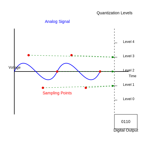
1.2 The Role of ADC in Modern Electronics
The advent of the analog-to-digital converter (ADC) has revolutionized modern electronics, making it an indispensable component in various applications across industries. By converting continuous analog signals into discrete digital data, ADCs facilitate the integration of analog systems with digital processing units, enabling effective data manipulation and analysis.
At the core of any digital system's operation lies the precise conversion of physical phenomena—such as temperature, pressure, and sound—into digital signals. For instance, in audio applications, microphones generate analog audio signals that must be transformed into digital data for processing, storage, or transmission. The effectiveness of this conversion directly impacts the system's fidelity, leading to significant advancements in sound quality in modern audio devices.
Applications Across Domains
In communications, ADCs are vital for converting radio signals into digitized formats for further processing in software-defined systems. This has paved the way for advanced wireless communication technologies such as LTE and 5G, which depend on the efficient transmission and reception of digital signals. Additionally, ADCs are crucial in sensors used in medical devices; for example, electrocardiograms (ECGs) digitize heart signals to enable precise diagnosis and monitoring.
Real-World Innovations Leveraging ADC
Consider smart home technologies: temperature and humidity sensors utilize ADCs to convert environmental readings into digital signals that are processed by microcontrollers. This data is vital for regulating HVAC systems efficiently, improving energy consumption, and enhancing user comfort. Furthermore, the integration of ADCs in wearable devices enables continuous monitoring of health metrics, fostering a proactive approach to health management.
The evolution of ADC technology has also introduced an array of architectures suitable for diverse applications. Techniques such as successive approximation, sigma-delta, and flash conversion each offer distinct advantages in terms of speed, resolution, and power consumption. For instance, flash ADCs are favored in applications requiring very high sample rates while successive approximation offers a good balance between speed and precision for many general-purpose applications.
Challenges and Future Directions
Nevertheless, integrating ADCs into modern systems is not without challenges. Issues such as quantization noise, non-linearity, and power consumption must be addressed to ensure high-performance outcomes. Researchers are continually exploring advanced techniques, such as using oversampling and noise shaping, to minimize these effects and improve overall performance.
Looking forward, the continuous advancement of ADC technology is crucial for the development of emerging fields including the Internet of Things (IoT), artificial intelligence (AI), and autonomous systems. As data acquisition and processing speeds increase, there's a growing demand for higher resolution and lower power consumption, positioning ADCs at the forefront of innovation in these domains.
In conclusion, the role of ADCs in modern electronics cannot be overstated. Their capability to bridge the gap between the analog and digital worlds enables seamless integration and advanced data processing across a multitude of applications.
2. Sampling
2.1 Sampling
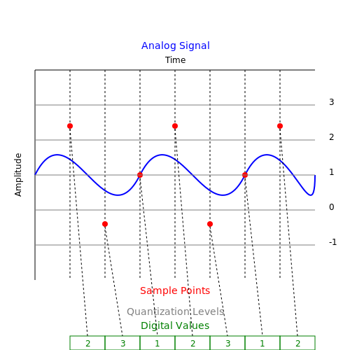
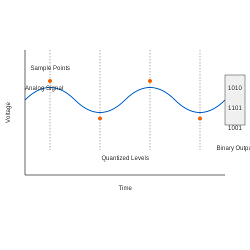
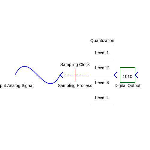
Sampling is a crucial process in the functioning of analog-to-digital converters (ADCs). It involves capturing the value of an analog signal at discrete intervals. The quality and integrity of the resultant digital representation depend heavily on how and when the analog signal is sampled. To understand this, we begin by examining the underlying principles and implications of the sampling process.
Understanding the Sampling Process
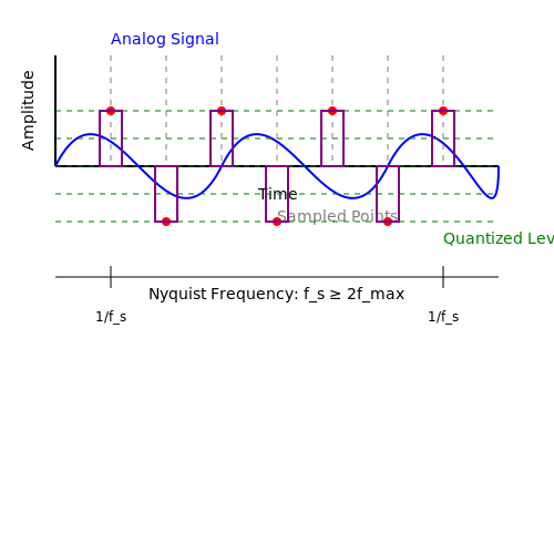
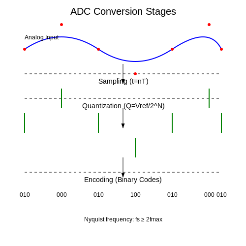
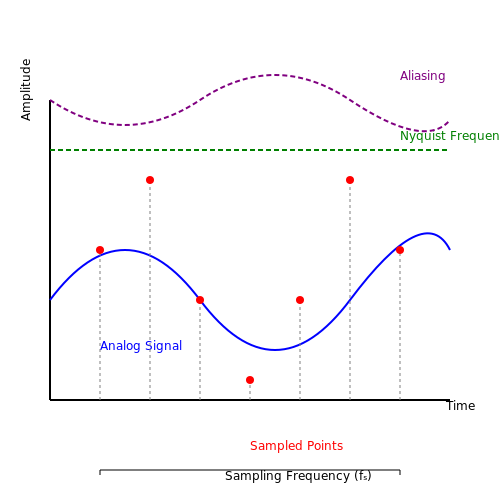
Sampling essentially converts a continuous analog signal into a discrete form by taking measurements at uniform time intervals. The chosen interval, also known as the sampling period (T), directly influences the fidelity of the conversion. To accurately reconstruct the original signal from its samples, the Nyquist-Shannon sampling theorem asserts that the sampling frequency (fs), which is the inverse of the sampling period, must be at least twice the highest frequency present in the analog signal (fmax):
Violation of this theorem leads to aliasing, where high-frequency components of the signal masquerade as lower frequencies, resulting in a distorted output. Therefore, selecting an appropriate sampling rate is paramount, particularly in applications where signal integrity is critical, such as audio processing, telecommunication, and biomedical signal acquisition.
Practical Considerations in Sampling
When implementing sampling in a circuit, several factors must be considered:
- Sampling Rate Selection: The choice of sampling rate is dictated by the nature of the signal. In practice, engineers often use a sampling frequency higher than twice the maximum signal frequency to accommodate real-world signal complexities and hardware limitations.
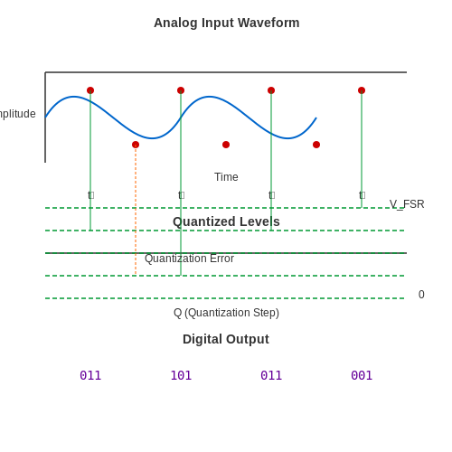
- Quantization Noise: Every sampled value must be quantized to a finite number of levels, introducing quantization error. The finer the quantization (more levels), the closer the digital signal approximates the original analog waveform.
- Anti-aliasing Filters: Before sampling, it is common to implement an anti-aliasing filter, which removes frequencies above half the sampling rate to prevent aliasing.
Real-World Applications of Sampling
Sampling is ubiquitous in modern technology. Here are a few noteworthy applications:
- Audio Processing: Digital music and voice recordings rely on high sampling rates to capture the nuances of sound accurately. For instance, CD audio is sampled at 44.1 kHz, providing frequencies up to 22.05 kHz, conforming to the Nyquist Criterion.
- Image Capture: Digital cameras sample light intensity across an array of sensor pixels, facilitating the creation of digital images. Here, the resolution and bit-depth of color quantization play critical roles in image fidelity.
- Medical Imaging: Imaging modalities such as MRI and CT scans depend on high sampling rates to reconstruct detailed internal views of the human body, thereby aiding in diagnostics and patient care.
In summary, sampling bridges the domain of continuous signals and discrete digital processing. The precise orchestration of this process significantly influences the performance, accuracy, and reliability of a multitude of electronic systems.
2.2 Quantization
Quantization is a fundamental process in analog-to-digital conversion (ADC), serving as the bridge between the continuous world of analog signals and the discrete realm of digital representation. At its core, quantization involves approximating a continuous signal by mapping it to a finite set of discrete levels. This process, while essential for digital signal processing, introduces certain implications that must be carefully considered, particularly in terms of signal fidelity and system performance.Understanding Quantization
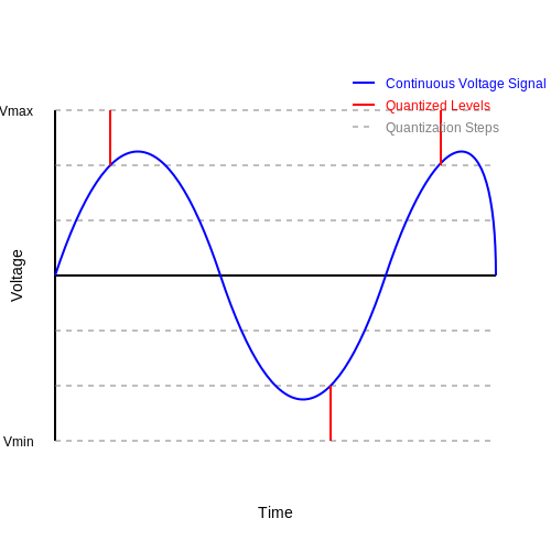
Quantization can be understood as the process of rounding the values of an analog signal to the nearest representable digital value. The number of discrete levels available for approximation is determined by the bit depth of the ADC. For instance, an ADC with a bit depth of \( n \) can represent \( 2^n \) distinct values. This establishment of discrete levels plays a critical role in determining the accuracy and resolution of the digital representation. To illustrate this, consider a simple case of an ADC with a bit depth of 3 bits. This ADC can represent \( 2^3 = 8 \) levels. If we have an analog signal that ranges from 0V to 5V, these discrete levels can be mapped to specific voltage intervals: - 0V to 0.625V → Level 0 - 0.625V to 1.25V → Level 1 - 1.25V to 1.875V → Level 2 - ...and so forth up to Level 7, which corresponds to 5V. The quantization error, defined as the difference between the actual analog value and the quantized digital value, directly affects the performance of an ADC. It is essential to recognize that quantization error introduces noise into the system, which can degrade signal quality. Thus, a critical balance must be struck between the resolution (related to bit depth) and noise floor.Mathematical Representation of Quantization
To formalize the quantization process, we can express the quantization operation mathematically. If \( x \) is the continuous analog input signal, the quantization function \( Q(x) \) can be defined as: $$ Q(x) = \Delta \cdot \text{round} \left( \frac{x}{\Delta} \right) $$ Where: - \( Q(x) \) is the quantized output, - \( \Delta \) is the quantization step size, calculated as \( \Delta = \frac{V_{max} - V_{min}}{L} \), with \( L = 2^n \) representing the number of quantization levels. This equation demonstrates how the continuous signal is converted into its nearest quantization level based on the defined step size. In practical applications, minimizing quantization error demands careful selection of both the ADC's bit depth and its sampling rate. One important consideration in designing systems involving quantization is the introduction of Quantization Noise. This noise, characterized by a uniform distribution within the range of \(-\frac{\Delta}{2}\) to \(+\frac{\Delta}{2}\), affects the system's Signal-to-Noise Ratio (SNR). The theoretical expression for the SNR in dB can be derived from this noise consideration: $$ SNR_{dB} = 6.02n + 1.76 $$ Where \( n \) is the number of bits. This relationship illustrates how increasing the bit depth effectively improves the SNR, thereby enhancing the accuracy of the digital signal representation.Practical Applications of Quantization
Understanding quantization is not merely an academic exercise; it has profound implications across various fields. In audio signal processing, for instance, higher bit depth ADCs capture more detail, improving the quality of digital sound in applications such as music recording and broadcasting. In imaging, quantization plays a crucial role in determining the dynamic range and color fidelity of digital photographs, impacting everything from smartphone cameras to professional digital imaging. Additionally, in telecommunications, quantization affects the overall performance of communication systems, particularly in the fidelity of transmitted signals. Engineers must consider the quantization levels when designing filters or error correction algorithms to maintain signal integrity. In summary, quantization epitomizes the interplay between analog and digital domains, carrying both opportunities for enhanced performance and challenges associated with noise and signal integrity. As technology continues to evolve, the understanding of quantization processes remains essential for engineers and researchers in fields that bridge the analog and digital worlds.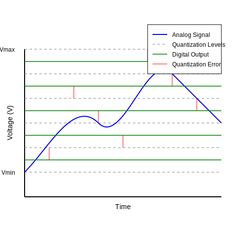
2.3 Encoding
The process of encoding within Analog-to-Digital Converters (ADCs) is fundamental in transforming an input analog signal into a discrete digital representation. Understanding the various encoding methods provides insights into the efficiency, accuracy, and overall performance of ADC systems. In this subsection, we will explore encoding methodologies, their significance in digital signal processing, and real-world applications.
Understanding Encoding
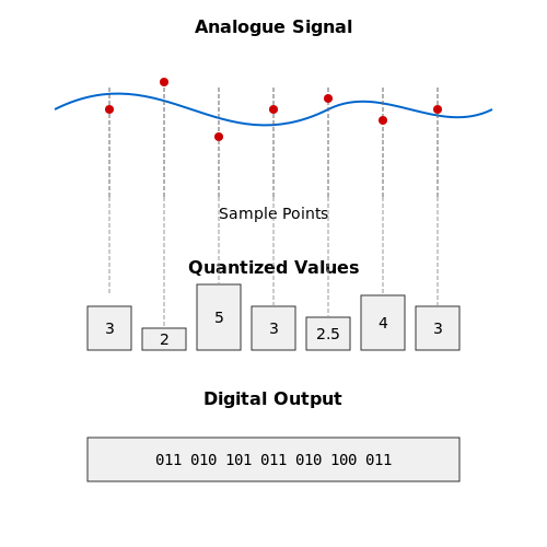
Encoding refers to the method by which ADCs assign binary values to quantized analog signal levels. This process is vital because the binary format is the standard representation for digital systems, allowing for high-speed processing and storage. Since signals can assume an infinite range of values, encoding also involves decisions about how to convert these values into a manageable number of discrete levels.
Several encoding schemes can be employed, with the most commonly used being Binary Encoding, Two's Complement Encoding, and Gray Code Encoding. Each method has its strengths and weaknesses depending on the application requirements.
Binary Encoding
In binary encoding, each quantized value is represented by a unique binary code. For an N-bit ADC, the number of quantization levels is \(2^N\), meaning each sample from the analog signal corresponds directly to its integer representation in binary format. For instance, a 3-bit ADC yields 8 quantization levels:
Binary encoding is straightforward and widely used due to its simplicity and efficiency in digital logic. However, it can be susceptible to errors, particularly in environments where signal integrity is paramount.
Two's Complement Encoding
Two's complement is particularly useful for representing negative values alongside positive values. Each negative analog signal level is stored as a binary number that complements its positive counterpart. For example, in a 4-bit two's complement system, the range can accommodate values from -8 to +7 as shown in the table below:
| Decimal Value | Binary Representation |
|---|---|
| -8 | 1000 |
| -7 | 1001 |
| -1 | 1111 |
| 0 | 0000 |
| 7 | 0111 |
This method excels in arithmetic operations but requires the ADC to include additional processing overhead.
Gray Code Encoding
Gray code represents signals where two adjacent values differ by only one binary digit. This characteristic minimizes the risk of error during transitions, making it particularly suited for rotary encoders and other applications where signal integrity during quantization is critical. For instance, the Gray encoding for a 3-bit system can be depicted as follows:
| Binary | Gray Code |
|---|---|
| 000 | 000 |
| 001 | 001 |
| 010 | 011 |
| 011 | 010 |
| 100 | 110 |
| 101 | 111 |
| 110 | 101 |
| 111 | 100 |
By reducing the potential for errors during value transitions, Gray code enhances the reliability of ADC outputs under dynamic conditions.
Real-World Applications
The choice of encoding scheme greatly influences ADC performance. For applications requiring fast arithmetic operations and efficiency—like digital signal processing in communication systems—binary encoding is ideal. Conversely, when precise position tracking is needed in robotics, Gray code is preferable due to its resilience to errors. Two’s complement is ubiquitous in audio and video processing, where both positive and negative signals are prevalent.
In summary, understanding different encoding methods paves the way for selecting the appropriate ADC design tailored to specific application needs. This knowledge is essential for engineers and researchers aiming to optimize signal acquisition systems in various fields.
3. Successive Approximation Register (SAR) ADC
3.1 Successive Approximation Register (SAR) ADC
The Successive Approximation Register (SAR) ADC is a vital component in modern electronic systems, bridging the gap between the analog and digital realms. It provides an efficient method for converting continuous signals to a discrete digital representation, making it invaluable in applications ranging from audio processing to industrial control systems. The fundamental operation of the SAR ADC is based on a binary search mechanism that achieves fast conversion while maintaining high accuracy.
Operational Principles of SAR ADC
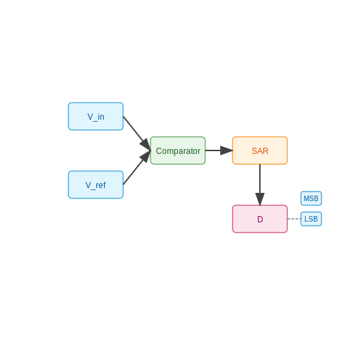
The SAR ADC employs a systematic approach to digitize an analog input voltage. It utilizes a binary search algorithm which operates through a series of steps that successively refine the approximation of the input voltage. This process begins with a reference voltage, typically the maximum allowable analog input, which is scaled down progressively until the closest digital representation is found.
At the heart of the SAR ADC is the successive approximation register itself, which is responsible for controlling the conversion process. The general steps involved are:
- The initial guess is set by loading the most significant bit (MSB) of the digital output to one.
- The comparator checks if the input voltage exceeds this reference voltage.
- Based on this comparison, the SAR either keeps the bit set or resets it, then moves to the next lesser significant bit.
- This cycle continues until all bits of the digital output are set or cleared.
This method allows the SAR ADC to convert an n-bit analog input into a digital output in n clock cycles, resulting in increased speed and reduced circuitry complexity compared to other types of ADCs, such as flash ADCs.
Mathematical Framework
To understand the performance of the SAR ADC, we can introduce some key equations. First, let’s denote the analog input voltage as Vin and the reference voltage of the ADC as Vref. The digital output, in an n-bit ADC, is calculated as:
Here, D represents the digital output value, which ranges from 0 to 2n - 1. This equation illustrates how the output voltage correlates directly with the input voltage and is influenced by the reference voltage.
Real-World Applications
SAR ADCs are widely used in various fields due to their balance of performance and efficiency. Common applications include:
- Data acquisition systems: SAR ADCs can accurately convert sensor outputs to digital signals for data processing.
- Audio applications: They facilitate high-quality audio digitization in sound processing environments.
- Industrial automation: In controlling systems where precision is critical, SAR ADCs deliver reliable measurements.
- Medical devices: They are pivotal in biomedical instruments, providing the required resolution and conversion speed.
Through their ability to accurately capture and convert analog signals, SAR ADCs play a significant role in advancing technology across various industries.
Conclusion
The Successive Approximation Register ADC stands out as a critical innovation in the field of analog-to-digital conversion. By employing a systematic approach through successive approximations, SAR ADCs combine speed, efficiency, and accuracy, making them an ideal solution for a myriad of applications. As technology continues to evolve, the role of SAR ADCs in developing high-fidelity electronic systems remains paramount.
3.2 Sigma-Delta ADC
The Sigma-Delta Analog-to-Digital Converter (ADC) is a sophisticated type of ADC that leverages oversampling and noise shaping to achieve high-resolution digital outputs. Unlike traditional ADCs which convert voltage levels directly, Sigma-Delta ADCs operate more like a modulator, emphasizing the importance of signal shape over mere voltage measurements.
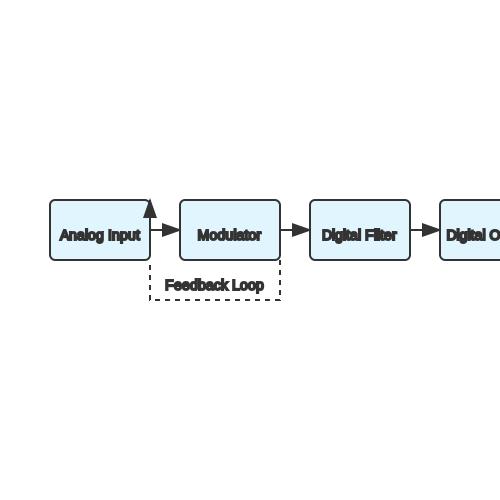
At its core, the Sigma-Delta ADC employs a feedback loop which incorporates a modulator and a digital filter. The fundamental operation begins with an analog signal being fed into a modulator that oversamples this signal, generating a 1-bit data stream. This process allows for a high degree of precision, primarily because the noise introduced during modulation can be shaped and filtered out.
Understanding Oversampling and Noise Shaping
To grasp the operational advantage of the Sigma-Delta ADC, we must first understand the concepts of oversampling and noise shaping. Oversampling refers to the practice of sampling the input signal at a frequency significantly higher than the Nyquist rate. This is mathematically beneficial because:
where \( f_{max} \) is the maximum frequency present in the signal. This technique enables the Sigma-Delta ADC to distribute quantization noise over a broader frequency range.
Noise shaping is where the inherent advantages of Sigma-Delta convertors become truly visible. The feedback loop in the modulator proactively controls the quantization noise. By implementing a second-order or higher feedback loop, a significant amount of the noise can be shifted to frequencies outside the bandwidth of interest, thereby enhancing the effective resolution of the converter.
Block Diagram of a Sigma-Delta ADC
As a visual reference, consider the following block diagram which illustrates the core components of a Sigma-Delta ADC:
Real-World Applications
The Sigma-Delta ADC is widely utilized in contexts that necessitate high accuracy and stability, particularly in applications such as:
- Audio Processing: Its high resolution and low noise make it ideal for digital audio converters.
- Medical Devices: In devices like digital X-ray and ECG machines, where precision is critical.
- Industrial Sensors: They are commonly found in applications that convert signals from thermocouples and pressure transducers.
In conclusion, the Sigma-Delta ADC is a powerful tool in the arsenal of modern electronics, being particularly well-suited for applications where high accuracy and precision are paramount. The sophisticated interplay between oversampling, noise shaping, and digital filtering enables it to achieve resolutions often unattainable in conventional conversion methods.
3.3 Flash ADC
The Flash ADC, also known as a parallel ADC, represents one of the fastest types of analog-to-digital converters available, making it a critical component in applications requiring high-speed signal processing. Unlike other ADC architectures such as successive approximation or integrating ADCs, the Flash ADC employs a unique mechanism that allows for instant conversion of an analog signal into its digital equivalent, hence its name.
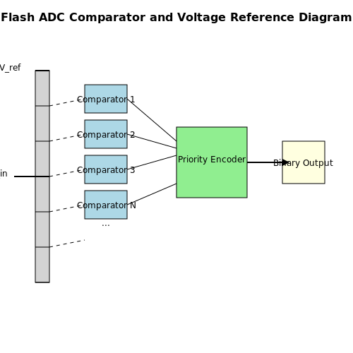
At its core, the Flash ADC utilizes a large array of comparators to determine the levels of the input voltage against predefined thresholds. These thresholds are typically created using a resistive ladder network, which divides the reference voltage (Vref) into a number of discrete steps. For a Flash ADC with N bits of resolution, this requires 2N - 1 comparators due to the fact that each comparator is responsible for one level of discrete voltage. As a result, a 4-bit Flash ADC would necessitate 15 comparators to cover the range from 0 to Vref adequately.
Understanding the Mechanism
The operation of a Flash ADC can be broken down into a few crucial steps. Firstly, the incoming analog voltage (Vin) is fed into all comparators simultaneously. Each comparator outputs a digital signal indicating whether Vin is greater than its respective reference level. The resulting outputs from the comparators are then encoded into a binary format by a priority encoder, which produces the final digital output.
This all occurs in a matter of nanoseconds, thus enabling the Flash ADC to achieve very high sampling rates. In fact, Flash ADCs can operate at speeds exceeding several gigasamples per second (GSPS), making them particularly suitable for high-frequency applications such as radar and video processing.
Advantages and Limitations
Flash ADCs are celebrated for their speed and simplicity in design. However, they also carry certain disadvantages. Notably, the need for a significant number of comparators increases the complexity and cost of the ADC design. Also, as the number of bits increases, the sensitivity to noise and offset errors becomes more pronounced, which can affect the accuracy of the conversion.
- High Speed: Flash ADCs are among the fastest available, capable of processing signals in the nanosecond range.
- Simplicity of Design: The straightforward architecture allows for rapid implementation into various systems.
- Large Area Requirement: The use of numerous comparators necessitates a larger chip area, which can limit integration into compact devices.
Applications
The rapid conversion speed of Flash ADCs makes them indispensable in a range of applications including:
- Video Signal Processing: Used in high-definition video processing to ensure instantaneous real-time adjustments to the signal.
- Radar Systems: Employed in military and aviation radar for precise distance measurement and target detection.
- High-Frequency Communications: Essential in digital communications where signals are modulated at high frequencies, ensuring minimal latency.
In summary, the Flash ADC is a striking example of a technology designed for unyielding performance at high speeds, balancing the need for speed with the complexities of analog signal processing and digital conversion. While they pose some challenges regarding power consumption and circuit complexity, the benefits often far outweigh the downsides in high-performance environments.
3.4 Dual Slope ADC
The Dual Slope Analog-to-Digital Converter (ADC) is a widely utilized conversion technique known for its high accuracy and noise resistance. It leverages a unique integration process that distinguishes it from other types of ADCs, primarily by its method of charging and discharging a capacitor. This section delves deeper into the operating principles, advantages, and practical applications of Dual Slope ADCs, giving a comprehensive overview appropriate for advanced practitioners in the field.
Working Principle
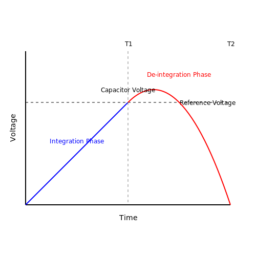
At the heart of the Dual Slope ADC is the integration of an analog signal over a specific period followed by a balancing process, where the capacitor is discharged at a reference voltage. This method allows for precise measurement of the input voltage by calculating the time it takes to discharge the capacitor back down to zero. The process is often broken into two primary phases: the integration phase and the de-integration phase.
Integration Phase
During the integration phase, the analog signal is fed into the ADC, where it causes the voltage across a capacitor to increase linearly. The integration time is governed by a clock signal, during which the output voltage ramps up. This can be described mathematically as:
Here, \( V_c(t) \) is the voltage across the capacitor, \( C \) is the capacitance, and \( I(t) \) is the input current. This phase continues until the clock signal indicates that the integration period is complete.
De-integration Phase
In the de-integration phase, a reference voltage (typically a known, stable voltage) is applied to discharge the capacitor. The time it takes to return to zero voltage is measured and is directly proportional to the magnitude of the input voltage during the integration phase. This can be represented by:
In this equation, \( t_d \) is the discharge time, and \( V_{ref} \) is the reference voltage used for the discharge. After the discharge cycle, the elapsed time is counted and translated into a digital output that corresponds to the original input voltage.
Advantages and Disadvantages
The Dual Slope ADC offers several notable advantages:
- High Accuracy: The averaging effect of the integration over time helps in mitigating the influence of noise, yielding higher accuracy in readings.
- Temperature Stability: The use of a reference voltage aids in improving temperature stability, which is critical for precision applications.
- Simple Design: Despite its sophisticated workings, the Dual Slope ADC can be less complex when compared to high-speed ADCs, making it easier to implement in various systems.
However, it is essential to consider its drawbacks:
- Conversion Speed: The Dual Slope ADC is typically slower than other types, like successive approximation or flash converters, making it less suitable for applications requiring rapid measurements.
- Components Sensitivity: The performance may be sensitive to the precision of the external components, such as the capacitor and resistors used.
Practical Applications
Despite its slow conversion rate, the Dual Slope ADC remains relevant, particularly in applications where precision is paramount. Common use cases include:
- Desktop Multimeters: Due to their requirement for high-resolution voltage measurements, Dual Slope ADCs are frequently used in digital multimeters.
- Industrial Measurement Systems: In environments where the electrical noise may impact performance, the noise-resistant characteristics of Dual Slope ADCs make them a good choice.
- Medical Equipment: Applications such as ECG or EEG machines benefit from the accuracy provided by these converters, ensuring precise data for diagnosis.
In conclusion, the Dual Slope ADC stands out in the realm of analog-to-digital conversion techniques, providing reliability and precision where it is most valued. For engineers and researchers, understanding its operation and applications can lead to more informed decisions in selecting the right ADC for their specific use cases.
4. Resolution
4.1 Resolution
The concept of resolution in Analog-to-Digital Converters (ADCs) plays a pivotal role in determining how finely an analog signal can be represented in the digital domain. Resolution refers to the smallest change in an analog input signal that results in a change in the output of the ADC. Understanding resolution is crucial for engineers and researchers as it directly impacts the fidelity of the digitized signal. To quantify resolution, one can look at the bit-depth of an ADC. The bit-depth is defined by the number of discrete levels into which the input voltage range can be divided. For instance, a typical 12-bit ADC can represent \(2^{12} = 4096\) distinct levels. This intrinsic relationship offers both theoretical and practical insights into the performance of the ADC. Mathematical Representation of Resolution The resolution \(R\) of an ADC can be mathematically expressed as follows: 1. Determine the full-scale range (FSR) of the ADC, denoted by \(V_{max} - V_{min}\). 2. The resolution can be expressed as: $$ R = \frac{V_{max} - V_{min}}{2^n} $$ where \(n\) is the number of bits of the ADC. For example, if an ADC has a voltage range from 0V to 5V and is 12-bit, the resolution calculated would be: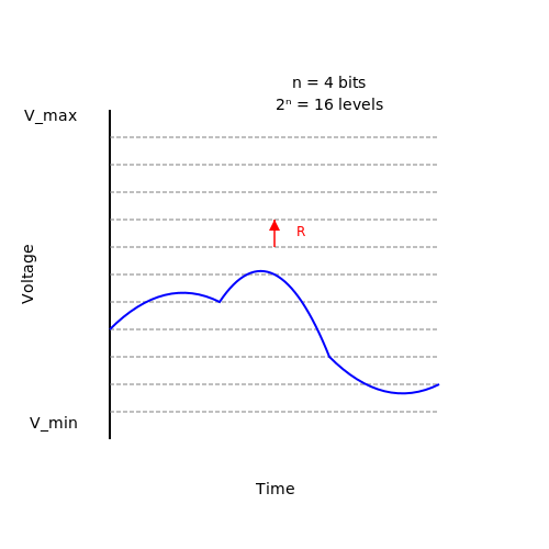
4.2 Sampling Rate
In the realm of Analog-to-Digital Converters (ADCs), the concept of sampling rate stands as a cornerstone, determining how effectively a continuous signal can be represented in digital form. This parameter dictates how frequently the analog signal is sampled per unit time, influencing both the resolution and fidelity of the digital representation. As we delve into this intricate subject, it's vital to appreciate the relationship between sampling rate, signal characteristics, and the inherent limitations dictated by the Nyquist-Shannon sampling theorem.The Nyquist Criterion
The Nyquist-Shannon sampling theorem states that in order to avoid aliasing—a phenomenon where different signals become indistinguishable when sampled—the sampling rate must be at least twice the highest frequency component of the signal. This minimum rate is known as the Nyquist rate. Mathematically, this can be expressed as:Impact of Sampling Rate on Signal Quality
When signals are sampled below their Nyquist rate, aliasing occurs, which introduces distortions that can obscure the original signal characteristics. On the other hand, sampling at higher-than-necessary rates results in increased data sizes, which can impose impractical demands on storage and processing systems. Hence, balance is paramount; finding the right sampling rate facilitates efficient data acquisition while ensuring signal integrity. Consider, for example, an audio signal containing frequencies up to 20 kHz. According to the Nyquist theorem, one would require a minimum sampling rate of 40 kHz to faithfully reconstruct the audio waveform. However, in practice, standard audio sampling rates, such as 44.1 kHz or 48 kHz, are often utilized to provide a margin of safety and handle any potential unforeseen frequency content.Quantifying Sampling Rate
In numerous applications, the sampling rate not only determines how the information is captured but also how quickly the ADC can produce digital output. This rate is typically described in samples per second (S/s) or Hertz (Hz). High-performance systems may require sampling rates in the megahertz (MHz) range, especially in fields like digital communications and high-speed signal processing. To further illustrate, the following equation provides a means of determining the minimum bandwidth \( B \) needed based on the desired sampling rate:Real-World Applications
In practical applications, the choice of sampling rate is influenced by several factors. In digital audio recording, a common practice is to employ a sampling rate of 44.1 kHz for music production and over 96 kHz for professional recordings. This ensures not only adherence to the Nyquist criterion but also provides sufficient headroom for the signal processing applied during mixing and mastering. Moreover, in industrial settings, data acquisition systems for sensor inputs often sample at rates around 1 kHz to 1 MHz, depending on the dynamics of the process or phenomena being monitored, such as vibration analysis or temperature fluctuations. Each sector has its performance benchmarks tailored to the specific requirements of accuracy, resolution, and data bandwidth.Conclusion
In summary, the sampling rate is pivotal in digital signal processing, dictating how analog signals are captured and represented in their digital form. The delicate balance between rate, signal integrity, and resource demands necessitates a deeper understanding among engineers and practitioners in the field. As technologies evolve and applications expand, mastering the intricacies of sampling rates will remain imperative to the advancement of high-fidelity signal processing systems.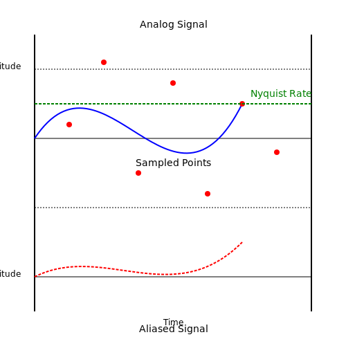
4.3 Signal-to-Noise Ratio (SNR)
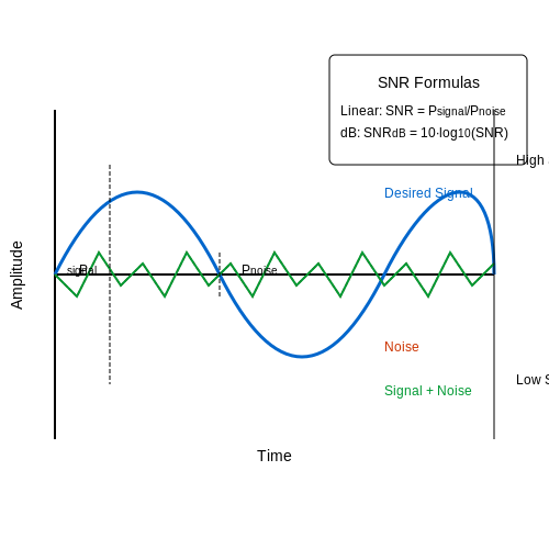
Signal-to-Noise Ratio (SNR) is a pivotal parameter in the realm of Analog-to-Digital Converters (ADCs), reflecting the quality of the signal being processed. It quantitatively describes the level of the desired signal relative to the level of background noise, serving as a vital indicator of the performance of an ADC. A higher SNR indicates a clearer signal, which is crucial for accurate digital representation.
Understanding SNR starts with recognizing that both the signal and noise can be represented in terms of their power. Mathematically, SNR is defined as:
Where:
- Psignal is the power of the desired signal.
- Pnoise is the power of the noise signal.
In many practical applications, especially in communication systems and measurement technologies, SNR is often expressed in decibels (dB). The conversion from a power ratio to decibels is achieved using the following expression:
Now, let's delve deeper into the implications of SNR in ADCs. The performance of an ADC can be significantly affected by the SNR, as it determines the quantization error and the overall fidelity of the digital representation of the analog signal.
Practical Implications of SNR in ADCs
In practice, SNR is influenced by various factors, including:
- Sampling Rate: Higher sampling rates can improve SNR but may also introduce more noise if the system bandwidth is not appropriately managed.
- Quantization Noise: Every time an analog signal is sampled, inherent quantization noise is introduced. An ADC with higher resolution (more bits) typically offers lower quantization noise, leading to improved SNR.
- Analog Signal Processing: Utilizing filters and amplifiers effectively can enhance the desired signal while suppressing noise, ultimately improving the SNR before it reaches the ADC.
Case Study: Real-World Application of SNR in ADCs
One prominent application of SNR assessment is in medical imaging devices, such as MRI machines. Here, it is vital to achieve high SNR to ensure accurate and detailed imaging of internal structures. Low SNR in MRI can lead to artifacts, making interpretation challenging. Techniques such as echo planar imaging enhance SNR significantly by optimizing the sampling strategy and sequence timing.
Understanding SNR and employing techniques to optimize it can dramatically enhance the effectiveness of ADCs. In telecommunications, for example, SNR is critical in defining the clarity of communication signals. As engineers design systems, balancing the SNR against other parameters like bandwidth and latency becomes essential for achieving optimal performance.
Ultimately, the vital role of SNR in ADCs encapsulates the interplay between signal fidelity and noise, guiding engineers and researchers toward innovations in signal processing technologies.
Linearity and Differentiation
In this subsection, we will delve into the key concepts of linearity and differentiation in the context of Analog-to-Digital Converters (ADCs). Understanding these concepts is crucial as they directly impact the performance and accuracy of the ADC in real-world applications, such as signal processing, instrumentation, and telecommunications.Linearity of ADCs
Linearity refers to the ability of an ADC to produce output codes that are proportional to the input voltage levels across its entire range. A perfectly linear ADC would have a transfer function that can be described as a straight line passing through the origin. In practice, this is not always the case due to several non-ideal effects such as quantization error, integral non-linearity (INL), and differential non-linearity (DNL). - Quantization Error: This error arises from the finite resolution of the converter. Each analog input level must be rounded to the closest digital output level, leading to a discrepancy. - Integral Non-Linearity (INL): This represents the deviation of the actual transfer function from the ideal linear function. It is typically specified as the maximum deviation in least significant bits (LSBs) across the entire range. - Differential Non-Linearity (DNL): DNL is concerned with the difference in width between the actual output levels. In an ideal ADC, the widths of the output states must be uniform. A DNL error indicates that the step sizes are not consistent.Mathematical Representation of Linearity
To assess linearity quantitatively, we can characterize it through a simple mathematical model. The idealized linear model can be expressed as: $$ V_{out} = k \cdot V_{in} \quad \text{for } V_{in} \in [0, V_{ref}] $$ where: - \( V_{out} \) is the digital output, - \( V_{in} \) is the analog input, - \( k \) is the scale factor dependent on the ADC resolution. To incorporate non-linearity, we can extend this equation to include a non-linear error term \( E(V_{in}) \): $$ V_{out} = k \cdot V_{in} + E(V_{in}) $$ Here, the error function \( E(V_{in}) \) accounts for both INL and DNL. Evaluating these characteristics is essential since they dictate the performance of the ADC in practical applications. An ADC with high linearity is desirable for applications requiring precise measurements, such as digital voltmeters, audio systems, and sensor interfacing.Differentiation in ADCs
Differentiation relates to how the ADC responds to changes in the input signal, which has pivotal implications for signal streaming and dynamic range applications. ADCs with rapid sampling rates must differentiate between quickly changing signal inputs effectively. When considering differentiation, two significant metrics emerge: sampling rate and anti-aliasing. The sampling rate determines how often the ADC captures the input signal. If the signal contains frequency components higher than half the sampling rate (the Nyquist limit), aliasing occurs, distorting the input signal representation. To effectively differentiate a waveform through an ADC, it is paramount to choose a suitable sampling rate based on the following: $$ f_{s} > 2 \cdot f_{max} $$ where \( f_{s} \) is the sampling rate, and \( f_{max} \) is the highest frequency present in the input signal.Practical Applications
In real-world scenarios, linearity and differentiation are critical during the design of signal processing networks. Poor linearity can lead to distorted signals, adversely affecting the detected data integrity in applications like radar systems or medical imaging. Conversely, sufficient differentiation ensures that rapid changes in the signal can be accurately captured, which is crucial in communications systems for high-speed data conversion.Visual Representation
To better understand the concepts of linearity and differentiation, consider a graph showcasing the ideal vs. actual transfer function of an ADC. The x-axis represents the analog input voltage, while the y-axis represents the digital output. The ideal linear graph is a straight line, while the actual response will exhibit deviations indicative of non-linearity.Conclusion
In summary, understanding the aspects of linearity and differentiation gives critical insights into ADC performance. Evaluating these parameters allows engineers and researchers to select the right ADC characteristics based on application requirements, ultimately leading to more reliable electronic designs and systems. With a robust understanding of these principles, the subsequent sections will explore ADC design considerations and further enhancements to optimize system performance.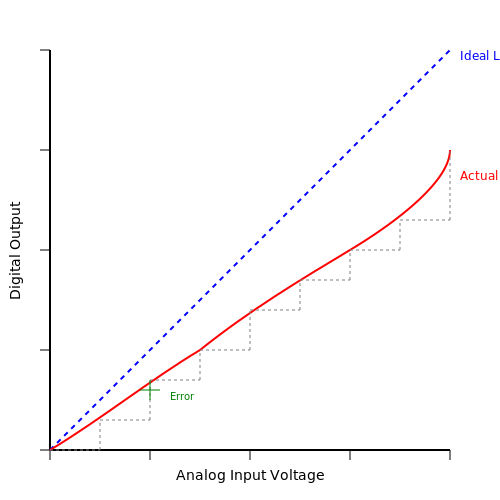
5. Audio Signal Processing
5.1 Audio Signal Processing
In the realm of electronics and signal processing, understanding how Analog-to-Digital Converters (ADCs) relate to audio signal processing is essential for developing modern audio applications—from music production to telecommunications. This subsection navigates the intricate relationship between ADCs and audio signals, elucidating key concepts and mechanisms.Understanding Audio Signals
At the most fundamental level, audio signals are analog waveforms representing sound. These waveforms can vary in amplitude, frequency, and phase, which correspond respectively to the volume, pitch, and characteristics of the sound being produced. To process these signals digitally—such as in a digital audio workstation (DAW) for music production—we rely on ADCs, which convert the continuous analog signals into discrete digital data. To appreciate the conversion process, consider the amplitude of an audio signal, which can be represented mathematically as a function of time, denoted by \( A(t) \). In many applications, this requires capturing the signal at specific intervals (sampling) and quantifying each sample to a set number of levels (quantization).The Sampling Theorem
The foundation of effective audio signal processing rests on the Nyquist-Shannon Sampling Theorem, which states that in order to accurately reconstruct an analog signal, it must be sampled at a frequency that is at least twice the highest frequency present in the signal. This frequency is referred to as the Nyquist rate, denoted as \( f_N \). In practical terms, for audio processing, this theorem dictates a minimum sampling rate of 44.1 kHz for standard CD audio, intended to capture frequencies up to 20 kHz, which reflects the upper limit of human hearing.Quantization and Bit Depth
Once the audio signal is sampled, each sample must be quantized, which entails mapping the sampled amplitudes to discrete values. The resolution of this quantization is determined by the ADC's bit depth; for instance, a 16-bit ADC can represent each amplitude with \( 2^{16} \) (or 65,536) distinct values. The quantization process introduces some error or distortion, referred to as quantization noise. To characterize the relationship between quantization error (\( e \)) and bit depth (\( n \)), we express the maximum quantization error as:Real-World Applications
The principles of ADC in audio signal processing are foundational to numerous real-world applications:- Music Production: Music studios utilize ADCs for converting live instruments and vocals into digital signals for editing and mixing.
- Telecommunications: Voice signals are digitally encoded for transmission over cellular networks, where ADCs are essential for converting sound waves into data packets.
- Speech Recognition: Devices like smartphones and smart speakers rely on ADCs to digitize speech for processing by natural language processing algorithms.
Conclusion
In summary, a robust understanding of audio signal processing and the role of ADCs is crucial for engineers and researchers in the field of electronics. By applying the principles of sampling, quantization, and bit depth, one can effectively manipulate audio data across various platforms and technologies, enhancing the clarity and quality of sound reproduction. With this foundation, we can proceed to explore specific implementations and advanced topics within the domain of audio signal processing, paving the way for innovation in sound technologies.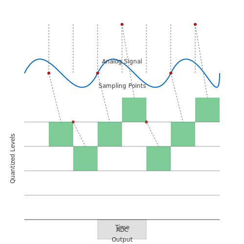
5.2 Image Processing
In the realm of electronics and signal processing, the concept of Analog-to-Digital Conversion (ADC) intertwines seamlessly with image processing, unleashing a plethora of applications that span from digital photography to computer vision. Image processing relies heavily on the conversion of continuous analog signals, harvested from sensors, into discrete digital values, which can then be manipulated and analyzed by powerful algorithms. An image can be viewed as a two-dimensional array of pixels, where each pixel possesses a specific value that corresponds to its intensity or color. The process begins when light hits the sensor—this could be a Charge-Coupled Device (CCD) or Complementary Metal-Oxide-Semiconductor (CMOS)—that generates an analog signal proportional to the intensity of light received. To delve into how ADC serves as a pivotal mechanism in image processing, we must consider the first critical step: quantization. In quantization, the continuous voltage reading from the sensor is sampled at discrete intervals. This fundamentally transforms the analog signal into a series of digital values. The performance of an ADC can be characterized by its bit depth, a parameter that dictates the number of discrete levels available for representation. The relationship is expressed as: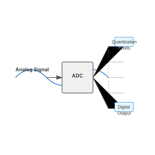
5.3 Data Acquisition Systems
Introduction to Data Acquisition
Data Acquisition Systems (DAS) play a pivotal role in collecting, analyzing, and processing signals from various sources. They convert real-world physical phenomena, such as temperature, pressure, and light, into digital data that can be manipulated and displayed. A fundamental component of a DAS is the Analog-to-Digital Converter (ADC), which bridges the analog world of sensors and signals to the digital realm of computers and data analysis software.
Core Components of a Data Acquisition System
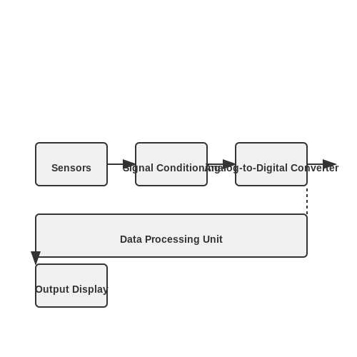
A typical data acquisition system consists of several key components:
- Sensors: Devices that convert a physical parameter (such as voltage, temperature, or pressure) into an electrical signal.
- Signal Conditioning: This includes amplification, filtering, and sometimes isolation to ensure that the signal is in a suitable form for the ADC.
- Analog-to-Digital Converter (ADC): Converts the conditioned analog signal into digital data.
- Data Processing Unit: Typically a microcontroller or a computer that processes the digital data for analysis.
- Output Interface: Displays the processed data, often in the form of graphs or logs for further review.
Signal Conditioning and Its Importance
Signal conditioning is crucial for enhancing the quality of signals prior to ADC conversion. It involves various techniques aimed at improving signal integrity. Notably, filtering removes unwanted frequency components, while amplification raises the signal level to match the ADC's input range. In cases where the source impedance is mismatched with that of the ADC, impedance matching using buffers can be critical to ensure accurate readings.
Understanding ADC Parameters
When selecting an ADC for a DAS, several parameters are vital to consider:
- Resolution: Defined by the number of bits of the ADC. Higher resolution allows for finer distinctions in the analog signal. For example, a 12-bit ADC can represent 4096 discrete values, while a 16-bit ADC can represent 65,536.
- Sampling Rate: Indicates how frequently the ADC can sample the input signal. Higher sampling rates can capture fast-changing signals but require more processing power and storage.
- Signal-to-Noise Ratio (SNR): This ratio helps in evaluating the quality of the conversion process. A higher SNR indicates a clearer and more accurate representation of the analog input.
Practical Applications of Data Acquisition Systems
Data acquisition systems find applications across various fields. In industrial automation, they monitor system performance, detect anomalies, and optimize processes. In environmental monitoring, they collect data on air quality, temperature, and humidity, crucial for understanding climate change impacts. Additionally, in medical applications, DAS are integral for monitoring patient vitals and ensuring accurate diagnostic measurements.
Case Study: Temperature Monitoring System
Consider a temperature monitoring system aimed at preventing overheating in industrial settings. The system includes thermocouples as sensors, an instrumentation amplifier for signal conditioning, and a high-resolution ADC. The digital output is processed in real-time, allowing operators to respond promptly to any dangerous temperature spikes, thereby increasing safety and efficiency within the facility. This case underlines the significance of effective data acquisition systems in industrial applications.
In conclusion, Data Acquisition Systems are indispensable in bridging the analog-digital divide, offering significant advantages in data quality and analysis capabilities. Understanding their components, operation, and application can enhance system design and functionality across various scientific and engineering domains.
6. Quantization Error
6.1 Quantization Error
When delving into the realm of Analog-to-Digital Converters (ADCs), one crucial concept that engineers and physicists must grasp is quantization error. This phenomenon directly impacts the accuracy and fidelity of digital representations of analog signals. Before exploring this topic in detail, it is essential to understand the quantization process. Quantization refers to the conversion of a continuous range of values into a finite range of discrete values. In the context of ADCs, this means mapping the infinitely varying input analog signal into a limited number of digital levels. For instance, an 8-bit ADC can produce 256 discrete levels, whereas a 12-bit ADC can represent 4096 distinct values. The choice of resolution significantly determines the granularity of the output signal. As we transition into the mathematical underpinnings of quantization error, we can observe that this error arises from the discrepancies between the actual analog signal and the quantized digital output. Specifically, the quantization error can be defined as the difference between the actual analog voltage (\(V_{in}\)) and the quantized voltage level (\(V_{out}\)). To delve deeper, consider that every time an analog signal is converted, there are distinct quantization levels defined by the formula: $$ V_{level} = \frac{V_{max} - V_{min}}{2^n} $$ Where: - \(V_{level}\) is the voltage step corresponding to each quantization level, - \(V_{max}\) and \(V_{min}\) are the maximum and minimum voltage values of the analog signal, - \(n\) is the number of bits used in the ADC. This indicates that the quantization error can be expressed mathematically as: $$ Q = V_{in} - V_{out} $$ Which can be bounded: $$ |Q| \leq \frac{V_{level}}{2} $$ This inequality reveals that the maximum quantization error is half of the voltage step, encapsulating the essence of quantization noise. Practically, as the number of bits in an ADC increases, the effective quantization error approaches zero, enhancing the resolution of the system and minimizing distortion in the output signal. In practical terms, quantization error manifests in various applications, such as digital audio and video processing, radar systems, and telecommunications. For example, in audio signal processing, higher bit depths (16-bit, 24-bit) are employed to capture a wider dynamic range and lower quantization noise, allowing for a more faithful reproduction of the original sound. To visualize the concept of quantization error, consider the following representation: imagine a continuous sine wave being tracked by distinct digital levels. Each segment of the sine wave that falls between two levels will be represented by either of those levels, introducing an error represented graphically as the vertical distance between the original waveform and the nearest quantization point.  In conclusion, understanding quantization error is pivotal for any advanced work involving ADCs. It not only enables finer control over signal representation but also informs the design choices that lead to optimal performance in various electronic applications. Future discussions will build upon this foundation by examining methods for mitigating quantization error and enhancing overall signal integrity in digital systems.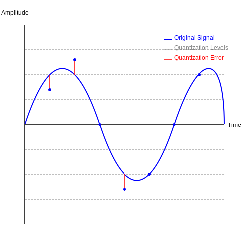
6.2 Aliasing
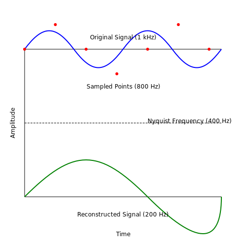
Understanding aliasing is crucial for engineers and researchers involved with analog-to-digital conversions (ADC). Aliasing occurs when a signal is sampled below its Nyquist frequency, leading to incorrect interpretations of the signal's frequency content. A comprehensive grasp of aliasing will enable you to make informed decisions when designing systems that utilize ADCs. The Nyquist theorem states that to accurately reconstruct a sampled signal, it must be sampled at a rate that exceeds twice its highest frequency component, known as the Nyquist frequency. Mathematically, if the highest frequency present in a signal is \( f_{max} \), then the sampling frequency \( f_s \) must satisfy- Loss of Information: Frequencies higher than half the sampling rate can produce misleading representations of the original signal.
- Design Complexity: Engineers must take care to design sampling systems that either avoid aliasing through higher sampling rates or implement filters to limit the frequency content before sampling, such as anti-aliasing filters.
6.3 Temperature Drift
Temperature drift represents one of the critical challenges in the design and application of analog-to-digital converters (ADCs). As electronic components heat up or cool down, their electrical properties—such as resistance, capacitance, and gain—often change. This variability directly impacts the accuracy and precision of ADC measurements, which is especially crucial in high-stakes applications like industrial automation, medical devices, and telecommunications.
In the context of ADCs, temperature drift refers to the change in the output value of the ADC (i.e., the digitized representation of the input signal) that occurs due to temperature variations. It can manifest in several forms:
- Offset Drift: This occurs when the output for a zero input (or any reference input) changes with temperature, effectively shifting the baseline of the signal.
- Gain Drift: Fluctuations in sensitivity or scale, where the ADC output corresponding to a known input signal deviates as temperature varies.
Understanding Temperature Drift
To analyze temperature drift quantitatively, we can employ a model that encapsulates both offset and gain drift. This is expressed mathematically through the following key equations:
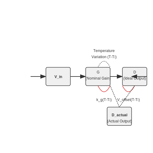
Assume we have an ideal ADC with a gain of \( G \) at a nominal temperature \( T_0 \). The digital output \( D \) for an input voltage \( V_{in} \) without drift can be expressed as:
Now, considering temperature drift, let the gain change with a temperature coefficient represented as \( k_g \) (in terms of volts per degree Celsius) and the offset shift represented as \( V_{offset} \). At temperature \( T \), the modified output can be approximated as:
Here, \( T \) is the operating temperature, \( T_0 \) is the reference temperature, and \( D_{actual} \) represents the output of the ADC after accounting for temperature effects.
Real-World Implications
The adverse impacts of temperature drift are particularly evident in high-precision measurement systems. Consider a medical instrumentation device that requires accurate temperature readings for patient monitoring. If the ADC used in such a device exhibits significant drift, the resulting errors could lead to misdiagnosis or inappropriate treatment. Thus, engineers must take care to minimize this effect through various means, including:
- Temperature Compensation: Implementing circuits or algorithms that automatically adjust the ADC output based on ambient temperature readings.
- Component Selection: Using components with low temperature coefficients to enhance the thermal stability of the ADC.
- Calibration Techniques: Regularly calibrating the ADC system to account for drift observed over time, especially in applications where environmental conditions vary widely.
Conclusion
The understanding and management of temperature drift are essential for the effective use of ADCs in many critical applications. By recognizing this phenomenon and designing accordingly, engineers can significantly enhance the performance and reliability of digital measurement systems.
7. Choosing the Right ADC for Your Project
7.1 Choosing the Right ADC for Your Project
When embarking on a project that requires analog-to-digital conversion (ADC), selecting the right ADC is paramount for achieving both performance and cost-effectiveness. An appropriate choice not only enhances efficiency but also ensures accuracy and reliability in data acquisition. As ADCs are critical in various fields, including telecommunications, medical devices, and instrumentation, a thorough understanding of the parameters involved is critical.Understanding ADC Specifications
Before diving into specific applications, let’s examine the basic specifications that should influence your choice. Typically, the following specifications need careful consideration:- Resolution: Indicated in bits, resolution defines the number of discrete values the ADC can output. A higher resolution leads to a finer granularity of the signal, thus improving accuracy. For instance, a 12-bit ADC offers 4096 discrete levels, while a 16-bit ADC offers 65536 levels.
- Sampling Rate: This specification illustrates how quickly the ADC can sample the input analog signal, expressed in samples per second (SPS). Depending on the application, you may need faster sampling rates for high-frequency signals.
- Input Voltage Range: This parameter specifies the maximum and minimum voltages the ADC can handle. Ensure the input voltage range aligns with your application’s expected signal levels to prevent clipping or distortion.
- Dynamic Range: This denotes the range of input signals an ADC can accurately convert, typically expressed in decibels (dB). A broad dynamic range is essential for detecting both high and low-level signals without distortion.
- Total Harmonic Distortion (THD): This specification is vital for applications in audio processing and RF signals. Low THD values indicate fidelity in the signal reproduction.
Application-Specific Considerations
Once you have a solid grasp of the specifications, it's essential to match these with the requirements of your specific application. For instance: - Medical Instruments: In medical applications like ECG monitoring, you may prioritize resolution and low noise to ensure accurate readings. A common choice in this domain might be a 24-bit ADC with a sample rate of at least 1 kSPS. - Audio Processing: Here, you will want an ADC with high sampling rates (44.1 kHz or greater) and low THD to support high-fidelity sound reproduction. - Industrial Automation: Applications might require fast sampling rates for real-time monitoring. For instance, an industrial sensor could demand an ADC with a sampling rate in the kHz range alongside decent resolution (10–16 bits).Cost versus Performance Trade-Off
While selecting an ADC, a crucial factor becomes balancing cost with performance. Most high-performance ADCs come at a premium, so determining your project’s acceptable performance threshold is vital. - If the project operates under a tight budget and the performances can be compromised, consider using a lower-resolution ADC with a fewer number of discrete steps. This can dramatically reduce costs without significantly degrading the required functionalities. - Conversely, if high accuracy and fidelity are non-negotiable due to regulatory standards—as seen in various sectors including aviation or healthcare—a higher-investment ADC may be necessary.Testing and Prototyping
After narrowing down your options based on specifications, applications, and costs, testing several ADC models in a prototyping phase is advisable. By comparing actual performance against datasheets and specifications in real-world scenarios, you can better assess the ADC’s functionality. - Evaluate aspects like thermal performance, nonlinearities, and noise factors that often do not make it onto specification sheets. Testing these factors ensures that the chosen ADC will perform adequately in the intended environment. In conclusion, choosing the right ADC for your project is a multifaceted decision requiring a careful assessment of specifications, applications, and trade-offs. By understanding these dimensions, you equip yourself with the knowledge to make an informed decision that aligns with your project’s objectives and constraints. Strong familiarity with the nuances of ADC operation will serve you well, ensuring you take full advantage of the powerful capabilities these devices offer.7.2 Interfacing ADCs with Microcontrollers
Understanding the interfacing of Analog-to-Digital Converters (ADCs) with microcontrollers is vital for engineers and researchers working across various application domains. Integrating these components allows for the effective conversion of analog signals from the environment into the digital domain, enabling microcontrollers to process and act on real-world data. This section will explore the principles and methodologies of interfacing ADCs with microcontrollers, placing a particular emphasis on practical implementation considerations.
Connection Methods
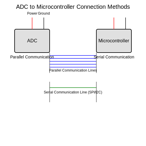
Two primary methods dominate the ADC to microcontroller interfacing landscape: parallel and serial communication.
- Parallel Communication: In this method, multiple data lines are used to transfer binary information simultaneously. This technique offers a faster data transfer rate due to the simultaneous nature of the connections. However, it requires a larger number of pins on the microcontroller, which may not be feasible for compact designs.
- Serial Communication: Serial connections, using protocols like SPI (Serial Peripheral Interface) or I2C (Inter-Integrated Circuit), send data one bit at a time over a single line. While this reduces the number of required pins, the communication speed can be a limiting factor.
Choosing the Appropriate Protocol
The choice between parallel and serial communication often depends on specific application requirements such as speed, complexity, and the number of available input/output (I/O) pins. For instance, high-speed applications such as digital oscilloscopes might favor parallel communication, while simpler sensors may work efficiently with I2C.
Data Acquisition and Control Mechanisms
Once the ADC is properly connected to the microcontroller, the next key aspect is understanding the data acquisition process. The ADC typically operates in a sample and hold mode:
- Sampling: The analog signal is sampled at discrete intervals, which must meet the Nyquist criterion to accurately reconstruct the original signal.
- Quantization: Each sample is converted into a digital number. The resolution of this conversion (often expressed in bits) plays a critical role in determining the fidelity of the digital representation.
Let’s delve deeper into the mathematical representation of the ADC process. The basic relationship governing the output of an ADC can be expressed as:
In this equation:
- D: The digital output (from 0 to 2n - 1, where n is the resolution in bits).
- Vin: The input analog voltage.
- Vref: The reference voltage against which the input is scaled.
- n: Number of bits of resolution, determining the granularity of the output.
This relationship underlines the critical nature of both the selection of Vref and the ADC’s resolution, as they directly affect the quality and accuracy of the digital output.
Real-World Applications
The principles of interfacing ADCs with microcontrollers extend across a broad spectrum of applications from consumer electronics to scientific instrumentation. Examples include:
- Automotive applications involving data acquisition from various sensors.
- Medical devices monitoring vital signs.
- Environmental sensing systems tracking temperature and humidity.
For any successful project utilizing ADCs, careful consideration must be given to both the hardware and software aspects to ensure seamless data handling and to achieve the desired performance metrics.
7.3 Filtering and Signal Conditioning
In the realm of analog-to-digital conversion (ADC), the integrity and quality of the sampled signal are crucial for accurate digital representation. Signal conditioning, which includes filtering, becomes an essential step in this process. Understanding the principles of filtering and the various types of filters can greatly enhance ADC performance.Understanding Signal Conditioning
Signal conditioning encompasses any manipulation of an electrical signal to make it suitable for processing. This step is particularly significant when interfacing sensors with ADC systems, where electrical noise and interference can distort the signal. By ensuring a clean, well-defined input, the ADC can produce a more precise digital output. Signal conditioning primarily adjusts the signal's amplitude, bandwidth, and impedance. Key techniques include amplification, level shifting, and filtering, each of which plays a vital role in preparing the analog signal for conversion. Among these techniques, filtering is essential for eliminating unwanted frequencies and noise from the signal before it is fed into the ADC.Filtering Defined
Filtering is a process that selectively removes or attenuates certain frequencies from a signal while allowing others to pass through. The choice of filter depends on the type of noise present and the characteristics of the desired signal. Several filter types can be employed in signal conditioning, including:- Low-pass filters (LPF): Allow frequencies below a certain cutoff frequency to pass while attenuating higher frequencies. They are particularly useful for removing high-frequency noise from a signal.
- High-pass filters (HPF): Permit frequencies above a specified cutoff frequency to pass while attenuating lower frequencies. They are typically used to eliminate DC offsets or low-frequency noise.
- Band-pass filters (BPF): Allow a specific range of frequencies to pass through while rejecting frequencies outside this range. BPFs are ideal for isolating specific signals from a broader spectrum.
- Notch filters: Designed to eliminate a narrow band of frequencies while passing all others. They are useful for excluding specific interference, such as the hum from electrical equipment.
Theoretical Background of Filters
Filter design typically involves defining transfer functions that describe how an input signal is transformed. The transfer function \( H(f) \) can be represented in the frequency domain, demonstrating the relationship between the input \( X(f) \) and output \( Y(f) \) as follows: $$ Y(f) = H(f)X(f) $$ Where: - \( Y(f) \) is the output signal in the frequency domain - \( H(f) \) is the frequency response of the filter - \( X(f) \) is the input signal in the frequency domain For a first-order low-pass filter, the transfer function can be expressed as: $$ H(f) = \frac{1}{1 + j\frac{f}{f_c}} $$ Where \( f_c \) is the cutoff frequency, and \( j \) is the imaginary unit. To derive its frequency response, we consider the magnitude and phase, given by: $$ |H(f)| = \frac{1}{\sqrt{1 + \left(\frac{f}{f_c}\right)^2}} $$ The filter's cutoff frequency \( f_c \) determines the frequency at which the output signal power falls to half its maximum value. This defines the effective filtering action of the low-pass filter.Real-World Application of Filters
In practical applications, filtering is crucial for enhancing ADC performance in various fields, such as biomedical instrumentation, audio processing, and industrial automation. For example, in ECG signal acquisition, the human body's electrical signals are often contaminated with electromagnetic interference. Employing a band-pass filter can help isolate the heart's activity from this noise. Similarly, in audio applications, low-pass filters are frequently used in digital signal processing to prevent aliasing effects by limiting the bandwidth before sampling. Each filter’s design and implementation depend on the specific requirements of the application, including the desired frequency response, linearity, and stability. In summary, filtering and signal conditioning are foundational components of effective ADC systems, playing a significant role in signal integrity and system performance. Understanding how different filters operate and applying them correctly can lead to substantial improvements in measurement accuracy and signal fidelity.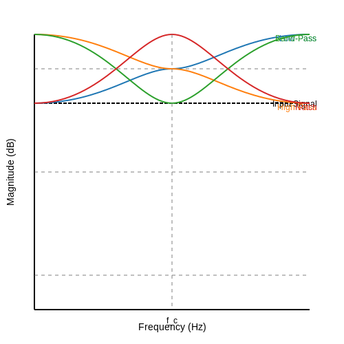
8. Increasing Resolution and Speed
8.1 Increasing Resolution and Speed
As we delve into the intricacies of Analog-to-Digital Converters (ADCs), the objectives of increasing resolution and speed become paramount, especially in advanced applications ranging from telecommunications to medical diagnostics. The interplay between these two parameters is fundamental to improving performance and accuracy in digital signal processing. To understand these enhancements, we must first define what we mean by resolution and speed. Resolution refers to the smallest increment of measurement or the number of discrete levels an ADC can output, typically represented in bits. A higher resolution means finer detail and a capability to distinguish smaller voltages in the input signal. Speed, on the other hand, is measured in samples per second (S/s) or conversions per second (C/s), signifying how quickly an ADC can process incoming signals. Achieving higher resolution often necessitates specific design considerations and architectural adjustments. In particular, the following techniques are commonly employed:Oversampling
Oversampling involves sampling an analog signal at a frequency significantly higher than the Nyquist rate (twice the highest frequency of interest in the signal). By averaging multiple samples, one can effectively improve resolution. Consider a scenario in which a 12-bit ADC outputs data from an analog input. If we oversample by a factor of 4, the effective resolution can be improved. This is mathematically expressed as:Delta-Sigma Converters
Delta-sigma (ΔΣ) ADCs are renowned for their ability to achieve high resolutions through oversampling. They utilize a feedback loop to minimize the distortion produced by quantization. The principle behind ΔΣ ADCs is to convert the analog signal into a high-frequency pulse-density-modulated signal. This high-frequency noise can then be filtered out, resulting in a much purer and more accurate lower-frequency signal output. The filtering and noise shaping techniques leveraged in ΔΣ converters contribute significantly to their performance, enabling resolutions of up to 24 bits and beyond with relatively low-speed designs. This architecture is particularly advantageous in audio applications and high-fidelity systems.Improving Speed
While resolution enhancement is crucial, increasing the speed of data acquisition is equally vital in situations demanding real-time digital signal processing. ADC speed improvements can be approached in various methods, including: - Parallel Conversion: Implementing concurrent conversion channels can significantly boost overall speed. Instead of relying on a single ADC, utilizing multiple ADCs working in tandem allows for simultaneous signal sampling. - Pipeline Architecture: Pipelined ADCs use multiple stages that enable data to be processed in a staggered fashion. By simultaneously processing different segments of the input signal, these architectures can drastically increase throughput while maintaining high resolution. - Reduced Latency Techniques: Employing techniques like direct sampling, where the signal is digitized immediately as it enters the ADC, helps lower latency, making the system more responsive. In practical applications, the choice between enhanced resolution or speed often requires a careful trade-off. For instance, in medical imaging systems, where detail is critical, higher resolution is typically favored. Conversely, in telecommunication systems, where data must be processed at high rates, speed becomes the priority. The synergy of resolution and speed plays a crucial role in applications such as radar systems, digital oscilloscopes, and high-speed data acquisition systems, where both characteristics directly influence the effectiveness of the technology. In conclusion, advancing the resolution and speed of ADCs requires a multifaceted approach, involving both technological innovations and architectural decisions. As we navigate these parameters, the balance between them will ultimately define the capacity of our electronic systems to handle increasingly complex and nuanced signals.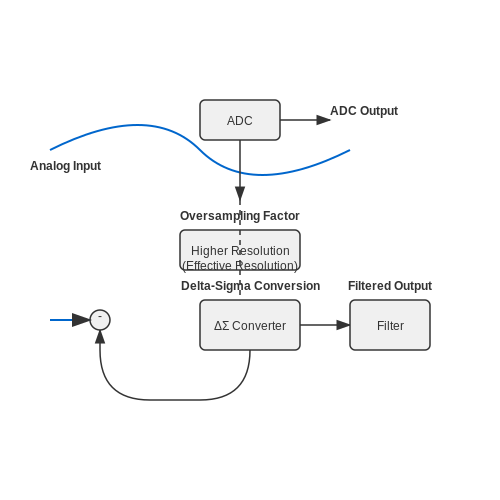
8.2 Integration with Other Components
When considering the role of an Analog-to-Digital Converter (ADC) within a broader electronic system, it is imperative to delve into its integration with various components. Understanding how an ADC interacts with other elements not only enhances the performance of digital systems but also improves overall functionality, enabling complex operations such as data acquisition, signal processing, and control systems.Interfacing with Sensors
The ADC's primary function is to convert analog signals from sensors into digital data that can be processed by microcontrollers or digital signal processors. Sensors, such as temperature, light, or pressure sensors, generate continuous electrical signals that need to be quantized by the ADC to be usable in digital formats. For example, a thermocouple sensor typically produces a millivolt-level signal that must be amplified to meet the input requirements of the ADC. This amplification not only ensures compatibility but also enhances the resolution of the temperature readings due to reduced noise levels.Signal Conditioning
Before the signal reaches the ADC, it often requires a process known as signal conditioning. This can involve:- Amplification: Increasing the signal strength to match the ADC's input range.
- Filtering: Removing high-frequency noise using low-pass filters or band-pass filters, ensuring that the ADC only processes desired frequency components.
- Level Shifting: Adjusting the voltage levels to fall within the ADC's acceptable input range, particularly important in multi-sensor systems.
Microcontroller Communication
Once an ADC has digitized the analog signal, the next step involves communication with a microcontroller (MCU). Most MCUs offer several communication protocols such as SPI (Serial Peripheral Interface) or I2C (Inter-Integrated Circuit). Each of these protocols has its pros and cons. For instance, SPI provides high-speed data rates and simpler hardware architecture, making it a strong candidate for applications requiring rapid data acquisition. Meanwhile, I2C allows for connecting multiple devices with minimal wiring at the cost of lower speeds. The choice of communication method will depend not just on data rate requirements but also on system complexity and flexibility. A microcontroller can then execute algorithms for data processing, storage, and analysis, paving the way for real-world applications in robotics, automation systems, and IoT (Internet of Things) devices.Integration into Control Systems
In control systems, the role of the ADC extends into feedback and signal processing for system stability. By converting real-world signals into digital data, the ADC aids in decision-making processes within digital controllers, enhancing performance in applications like motor control, temperature regulation, or active suspension systems. The implications of ADC integration in control systems can be illustrated through a simple feedback loop. The digital signal from the ADC feeds into a controller, which then adjusts an actuator based on predefined parameters to maintain desired operating conditions, such as a specific temperature or position. Feedback loops enhance system reliability and accuracy, critical in fields such as aerospace and automotive systems.Case Study: Data Acquisition Systems
Data acquisition systems (DAS) are a prime example of ADC integration where multiple sensor inputs are converted into digital formats for analysis. In these systems, ADCs must operate under varying conditions, making attributes such as sampling rate, resolution, and noise performance critical. Consider a multi-channel DAS monitoring environmental parameters. Each sensor's output must be conditioned appropriately and subsequently digitized by the ADC. The processed data can be analyzed in real-time to detect anomalies, trends, or changes in conditions, facilitating timely decision-making in fields like environmental monitoring or industrial automation. In conclusion, the integration of ADCs with other components, particularly sensors and microcontrollers, is foundational for the functionality of modern electronic systems. Understanding these relationships will allow engineers and researchers to design more efficient and robust systems across various applications.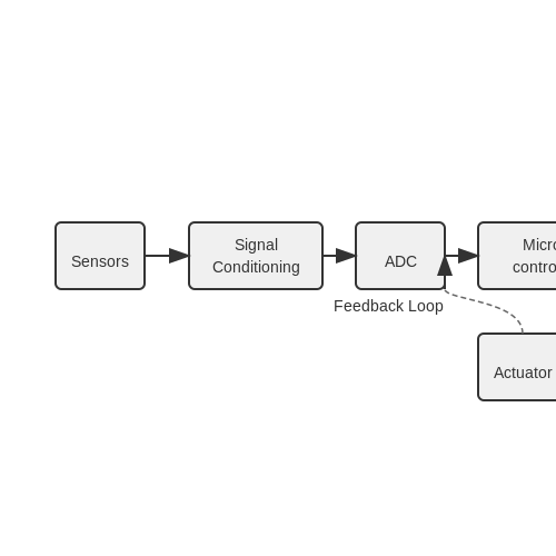
8.3 Emerging Applications
Within the realm of electronics, the significance of Analog-to-Digital Converters (ADCs) has skyrocketed as technology pushes toward greater integration and efficiency. This subsection uncovers the emerging applications of ADCs, exploring their critical roles in fields such as healthcare, telecommunications, and renewable energy.
Advancements in Healthcare Technology
In healthcare, the integration of ADCs in medical devices has transformed patient monitoring and diagnostics. Wearable health technology, such as glucose monitors and heart rate sensors, relies on ADCs to translate analog signals into digital data that a microcontroller can process.
For instance, a continuous glucose monitor (CGM) uses analog sensors to detect glucose levels in interstitial fluid. These analog signals are converted by high-resolution ADCs, allowing for real-time data processing and analysis. The application of high-resolution ADCs (up to 24-bit precision) enhances the accuracy of readings, which can significantly affect patient care decisions.
Wireless Communication and Data Transmission
In telecommunications, ADCs serve as essential components in various systems, from smartphones to satellite communication. They facilitate the process of capturing and converting analog signals transmitted over the air into digital formats that can be efficiently processed and transmitted. This conversion is crucial for applications such as:
- 4G/5G Networks: ADCs enable higher data rates and improved signal integrity, essential for modern high-speed mobile networks.
- Software-Defined Radio (SDR): By digitizing radio signals, ADCs allow for more flexible and adaptable communication systems based on software algorithms.
The shift toward digital wireless communication also underscores the importance of low-latency ADCs. As the demand for instantaneous data transfer grows, ADC architectures that minimize conversion time and maximize bandwidth are increasingly pursued.
Renewable Energy Systems
As society increasingly shifts towards renewable energy sources, ADCs play a pivotal role in optimizing the performance of solar panels and wind turbines. In photovoltaic systems, ADCs measure voltage and current levels to evaluate power generation efficiency. They enable Maximum Power Point Tracking (MPPT) algorithms that adjust the load conditions to harvest the maximum available power from the solar panels.
Moreover, in wind energy applications, ADCs facilitate the monitoring of environmental conditions, such as wind speed and direction, thus allowing for adaptive control of the turbine systems. These integrations help maximize energy extraction and ensure that the systems operate within safe parameters.
Innovations in Consumer Electronics
Consumer electronics are rapidly evolving towards more intelligent devices that utilize ADCs extensively. Innovations such as smart speakers and augmented reality (AR) devices rely on high-performance ADCs to digitize audio signals and environmental data effectively. For instance:
- Smart Speakers: Utilize multiple high-resolution ADCs to process voice commands accurately and reproduce sound in high fidelity.
- AR Devices: Rely on ADCs to capture spatial data, enhancing the interaction between digital and physical environments.
The precise functionality of ADCs in these various applications illustrates their integral role in shaping modern technological landscapes, providing bridges between analog phenomena and digital solutions. As innovations continue to proliferate, the evolution and enhancement of ADC technologies will undeniably drive further advancements across multiple domains.
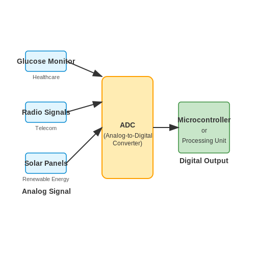
9. Recommended Books
9.1 Recommended Books
- Analog-to-Digital Conversion by Marcel Pelgrom — This book offers a comprehensive guide on the principles and operation of ADCs, addressing key concepts from noise shaping to oversampling, making it perfect for researchers and engineers seeking in-depth technical knowledge.
- Data Conversion Handbook by Walt Kester — The book provides insights and practical information on data conversion techniques, blending foundational theory with real-world applications, ideal for advanced-level readers involved in high-precision projects.
- Analog Circuit Design by Rudy J. van de Plassche — Aimed at advanced professionals, this text explores the intricacies of analog circuit design with an emphasis on ADCs and DACs, delving into the mathematical underpinnings of each component.
- CMOS: Mixed-Signal Circuit Design by R. Jacob Baker — A detailed exploration of mixed-signal design, including extensive coverage of ADC circuits within CMOS technology, making it essential for those looking to innovate within the semiconductor industry.
- A/D and D/A Converter Design by M.H. Zaki — This resource provides a systematic approach to converter design, offering insights into architectural choices and system integration challenges faced during the engineering process.
- IEEE Std 1241-2010: Standard for Terminology and Test Methods for Analog-to-Digital Converters — A definitive standard providing a universal framework for terminology, testing, and classification of ADCs, invaluable for engineers ensuring compliance with industry benchmarks.
- Digitally Assisted, Fully Integrated, Wideband Transmitters for High-Speed Millimeter-Wave Wireless Communication Links — Though primarily focusing on transmitters, this book includes detailed discussions on ADC requirements for high-speed digital communications, crucial for developing next-generation wireless systems.
- Time-interleaved Analog-to-digital Converters: Lab Demonstrations and a Hands-on Learning Approach — An excellent tool for those seeking a practical understanding of time-interleaved ADC systems, featuring lab demonstrations and hands-on exercises to bridge the gap between theory and practice.
9.2 Academic Journals
In this section, we will explore a curated list of academic journals that provide advanced insights into Analog-to-Digital Converters (ADC). These resources are particularly useful for engineers, physicists, and researchers seeking to deepen their understanding of ADC technologies and applications.- A Comprehensive Review of ADC Architectures — This IEEE article offers an in-depth review of various ADC architectures, focusing on their design principles, performance metrics, and exemplary applications in modern electronics.
- IEEE Transactions on Circuits and Systems II — This journal publishes research papers focused on the latest advances in integration technologies of digital systems, including groundbreaking studies on ADC design and implementation.
- Journal of Solid-State Circuits — Known for articles on cutting-edge solid-state circuit theories and practices, this journal includes innovative ADC research crucial for understanding advancements in circuit integration.
- Microelectronics Journal — A well-regarded publication for research in the microelectronics field, providing extensive analysis on ADC trends, design techniques, and integration strategies.
- Proceedings of the IEEE — This prestigious journal offers in-depth reviews and surveys on emerging areas of current interest to researchers in ADC technology and other electronic systems.
- Analog Integrated Circuits and Signal Processing — Features scholarly articles on the design, development, and implementation of ADCs, focusing on techniques for enhancing signal processing in analog circuits.
- International Journal of Circuit Theory and Applications — Offers comprehensive research articles and review papers on circuit theory, including detailed discussions on improving ADC technologies.
9.3 Online Resources
- Analog Devices Education Library — Offers a myriad of resources on ADCs and related concepts, including datasheets, technical guides, and tutorials crafted by experts in analog and mixed-signal technologies.
- Selecting ADCs for Your Application — A focused application note from Maxim Integrated detailing the considerations when choosing an ADC, complete with examples and real-world applications.
- EE Times - Introduction to ADCs — Provides an introductory overview of ADCs, their function, and characteristics with early insights into the history and technological advancements in ADCs.
- Texas Instruments - Understanding Data Converters — An extensive whitepaper that breaks down the architecture and operational principles of data converters, including ADCs, with a focus on design and performance optimization.
- Microchip Technology - ADC Solutions — A comprehensive resource hub featuring ADC-centric microcontroller applications, development kits, and prototypes aimed at smoothing out ADC integration in embedded systems.
- ResearchGate - ADC for Microcontroller Applications — Scholarly articles on the employment of ADCs in microcontroller applications with empirical data and theoretical analysis relevant for both academic and industrial contexts.
- EDN Network - Things You Need to Know About ADCs — A multi-part article series simplifying the knowledge needed to comprehensively understand ADC architectures, offering clear visuals and theoretical insights.
- DigiKey - Understanding ADCs — An instructional article that breaks down the fundamental operation and specifications of ADCs for engineers designing systems for precise data conversion.