Op-Amp Basics
1. Definition and Key Characteristics
1.1 Definition and Key Characteristics
An operational amplifier (op-amp) is a high-gain, DC-coupled differential amplifier with a single-ended output. Its behavior is primarily governed by negative feedback, enabling precise control over gain, bandwidth, and linearity. The ideal op-amp model assumes infinite gain, infinite input impedance, zero output impedance, and infinite bandwidth—though real-world devices exhibit deviations.
Fundamental Properties
The op-amp's transfer function is expressed as:
where AOL is the open-loop gain (typically 105 to 106), and V+, V- are the non-inverting and inverting inputs, respectively. In practical circuits, feedback networks reduce the effective gain to a finite, stable value:
where β is the feedback factor.
Non-Ideal Characteristics
Real op-amps exhibit critical limitations:
- Input Offset Voltage (VOS): A small DC voltage (µV to mV) required to null the output, caused by transistor mismatches.
- Common-Mode Rejection Ratio (CMRR): Measures the ability to reject signals common to both inputs, typically 70–120 dB.
- Slew Rate: The maximum rate of output change (V/µs), limiting large-signal bandwidth.
- Gain-Bandwidth Product (GBW): For a frequency f, the closed-loop bandwidth is GBW/ACL.
Practical Implications
In precision instrumentation, VOS and CMRR dictate accuracy, while slew rate and GBW define dynamic performance. For example, audio amplifiers require high slew rates (>20 V/µs) to avoid distortion, whereas sensor interfaces prioritize low VOS.
Symbol and Pin Configuration
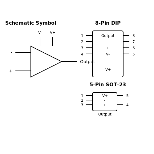
The operational amplifier (op-amp) is universally represented in schematics by a triangular symbol, denoting its high-gain differential amplification behavior. The standard symbol consists of two inputs—inverting (−) and non-inverting (+)—and a single output, with power supply pins often omitted in simplified diagrams but critical for practical implementation.
Standard Op-Amp Symbol
The idealized op-amp symbol includes:
- Non-inverting input (+): A positive voltage change here produces an in-phase output.
- Inverting input (−): A positive voltage change here produces an output 180° out of phase.
- Output: High-impedance node delivering the amplified differential input signal.
Physical Pin Configuration
Real-world op-amps (e.g., 741 in an 8-pin DIP package) follow standardized pinouts:
- Pin 2: Inverting input (−)
- Pin 3: Non-inverting input (+)
- Pin 6: Output
- Pins 7 and 4: Positive (VCC) and negative (VEE) supply rails
- Pins 1 and 5: Offset null for precision calibration
Power Supply Considerations
Op-amps require symmetric dual supplies (e.g., ±15V) or single-supply operation with biasing. The open-loop gain AOL is derived from the internal transistor stages:
where V+ and V− are the non-inverting and inverting input voltages, respectively. Modern rail-to-rail op-amps minimize headroom constraints by allowing inputs and outputs to operate near supply rails.
Historical Context
The triangular symbol originated from analog computers in the 1940s, where op-amps performed mathematical operations. The 741’s pinout (introduced by Fairchild in 1968) became an industry standard, influencing subsequent IC designs.
1.3 Ideal vs. Real Op-Amps
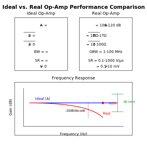
The operational amplifier (op-amp) is often analyzed under idealized assumptions, but real-world devices exhibit deviations that must be accounted for in precision circuit design. Understanding these differences is critical for applications requiring high accuracy, stability, and bandwidth.
Ideal Op-Amp Characteristics
An ideal op-amp is defined by the following characteristics:
- Infinite open-loop gain (AOL): The output voltage is unbounded for any differential input.
- Infinite input impedance: No current flows into the input terminals.
- Zero output impedance: The output can drive any load without signal degradation.
- Infinite bandwidth: No frequency-dependent roll-off in gain.
- Zero input offset voltage (VOS): The output is exactly zero when inputs are equal.
- Zero noise: No thermal or flicker noise contributions.
These assumptions simplify circuit analysis but are unattainable in practice.
Real Op-Amp Non-Idealities
Finite Open-Loop Gain and Bandwidth
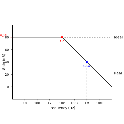
Real op-amps exhibit a finite open-loop gain, typically ranging from 104 to 106, and a frequency-dependent roll-off due to internal compensation. The gain-bandwidth product (GBW) describes this relationship:
where AOL is the DC open-loop gain, f is the frequency, and fc is the corner frequency. The GBW is constant for frequencies above fc:
Input Offset Voltage and Bias Currents
Mismatches in the input stage transistors produce an input offset voltage (VOS), typically in the range of µV to mV. Additionally, input bias currents (IB+ and IB-) flow into the terminals due to finite input impedance. The input offset current (IOS) is the difference between these:
These errors can be mitigated with external trimming or chopper-stabilized designs.
Output Impedance and Slew Rate
Real op-amps have non-zero output impedance (Zout), typically between 10 Ω to 1 kΩ, which affects load driving capability. The slew rate (SR) limits the maximum rate of output voltage change:
This is determined by internal compensation capacitance and bias currents.
Practical Implications
In precision applications such as instrumentation amplifiers or active filters, these non-idealities introduce errors:
- Gain error: Finite AOL reduces closed-loop gain accuracy.
- Phase margin: Limited bandwidth can cause instability in feedback networks.
- DC errors: VOS and IB create output offsets.
Modern op-amps, such as auto-zero or precision types, minimize these effects but require careful PCB layout and supply decoupling.
2. Inverting Amplifier
2.1 Inverting Amplifier
The inverting amplifier configuration is one of the most fundamental op-amp circuits, providing precise voltage gain with a phase inversion. Its operation relies on negative feedback to stabilize the gain while maintaining high input impedance and low output impedance.
Circuit Analysis
The standard inverting amplifier consists of an operational amplifier with two resistors: R1 (input resistor) and Rf (feedback resistor). The non-inverting input is grounded, while the inverting input forms a virtual ground due to the op-amp's high open-loop gain.
Voltage Gain Derivation
Applying Kirchhoff's current law at the inverting input (virtual ground):
Solving for the closed-loop voltage gain Av:
The negative sign indicates phase inversion. The gain depends solely on the resistor ratio, making it stable against op-amp parameter variations.
Input and Output Impedance
The input impedance is approximately R1, as the virtual ground presents a low-impedance node. The output impedance remains very low (typically <1Ω) due to the op-amp's negative feedback.
Practical Considerations
- Bandwidth limitations: The gain-bandwidth product (GBW) of the op-amp affects frequency response
- Resistor selection: Values between 1kΩ-100kΩ balance noise, power, and bias current effects
- DC offset: Input bias currents may require a compensation resistor on the non-inverting input
Advanced Applications
Inverting amplifiers form the basis for more complex circuits:
- Summing amplifiers (multiple inputs)
- Integrators (capacitor as feedback element)
- Transimpedance amplifiers (photodiode receivers)
2.2 Non-Inverting Amplifier
The non-inverting amplifier configuration is a fundamental op-amp circuit that provides a voltage gain greater than unity while preserving the phase of the input signal. Unlike the inverting amplifier, the input signal is applied directly to the non-inverting terminal, making the input impedance extremely high—a critical advantage in many applications.
Circuit Configuration and Operation
The basic non-inverting amplifier consists of an operational amplifier with a feedback network formed by resistors R1 and Rf. The input signal Vin is connected to the non-inverting terminal (+), while the inverting terminal (-) is tied to a voltage divider between the output and ground.
Gain Derivation
Using the ideal op-amp assumptions (infinite input impedance, zero output impedance, and infinite open-loop gain), the voltage at the inverting terminal must equal the voltage at the non-inverting terminal due to negative feedback. Applying Kirchhoff's current law at the inverting node:
The feedback current through Rf and R1 creates a voltage divider relationship:
Setting these equal and solving for the closed-loop gain Av:
Practical Considerations
Input Impedance: The non-inverting configuration exhibits extremely high input impedance, typically in the gigaohm range for modern FET-input op-amps, making it ideal for sensor interfaces and high-impedance signal sources.
Bandwidth Limitations: The gain-bandwidth product (GBW) of the op-amp imposes a frequency-dependent roll-off. For an op-amp with GBW = 1 MHz, a closed-loop gain of 100 will yield a bandwidth of approximately 10 kHz.
Noise Performance: The non-inverting configuration tends to have better noise performance than the inverting amplifier because the signal path doesn't flow through the feedback resistors. However, resistor thermal noise and op-amp voltage noise still contribute to the total output noise.
Advanced Applications
Voltage Buffers: When Rf = 0 and R1 → ∞, the circuit becomes a unity-gain buffer (Av = 1), used for impedance transformation without voltage amplification.
Precision Instrumentation: The high input impedance makes this configuration ideal for medical instrumentation, strain gauge amplifiers, and other applications where minimal signal loading is critical.
Composite Amplifiers: Multiple non-inverting stages can be cascaded to achieve higher gains while maintaining phase coherence, though stability must be carefully analyzed using Bode plots or Nyquist criteria.
2.3 Differential Amplifier
The differential amplifier is a fundamental op-amp configuration that amplifies the difference between two input signals while rejecting common-mode signals. Its ability to suppress noise and interference makes it indispensable in precision instrumentation, medical electronics, and communication systems.
Basic Operation
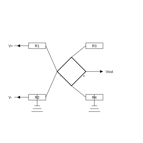
A differential amplifier consists of two matched input paths, where the output voltage Vout is proportional to the difference between the non-inverting (V+) and inverting (V−) inputs. The transfer function is derived using superposition:
where Ad is the differential gain and Acm is the common-mode gain. An ideal differential amplifier has Acm = 0.
Circuit Analysis
The standard implementation uses a resistor network to set the gain. For a balanced differential amplifier with resistors R1 and R2:
When R3 = R1 and R4 = R2, the equation simplifies to:
Common-Mode Rejection Ratio (CMRR)
The effectiveness of a differential amplifier is quantified by its CMRR, defined as:
High CMRR (typically >80 dB) ensures robust noise rejection. Mismatched resistors degrade CMRR, necessitating precision components or trimming in critical applications.
Practical Considerations
- Input Impedance: Non-inverting inputs should have matched impedance to avoid common-mode bias errors.
- Bandwidth: Gain-bandwidth product (GBW) limitations affect high-frequency performance.
- DC Offsets: Input bias currents can introduce output errors, mitigated by bias compensation resistors.
Applications
Differential amplifiers are pivotal in:
- ECG/EEG systems for rejecting 50/60 Hz interference.
- Balanced audio lines to eliminate ground loop noise.
- Wheatstone bridge interfaces for strain gauges and load cells.
2.4 Summing Amplifier
The summing amplifier, a fundamental application of operational amplifiers, performs weighted addition of multiple input signals. Its output voltage is a scaled sum of the input voltages, with each input's contribution determined by the ratio of feedback and input resistances.
Circuit Configuration
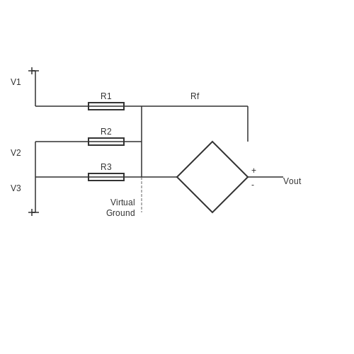
A summing amplifier extends the inverting amplifier configuration by incorporating multiple input branches. Each input voltage Vn connects to the inverting terminal through a corresponding resistor Rn, while a single feedback resistor Rf connects the output to the inverting input. The non-inverting terminal is grounded.
Mathematical Derivation
Applying Kirchhoff's current law at the inverting terminal (virtual ground):
Solving for Vout yields the general summing amplifier equation:
For equal input resistors (R1 = R2 = ... = Rn = R), the expression simplifies to:
Practical Considerations
Key design parameters include:
- Input impedance: Each input branch presents impedance Rn to its signal source
- Bandwidth limitations: The finite gain-bandwidth product affects high-frequency performance
- Noise contributions: Thermal noise increases with additional input branches
- DC offsets: Input bias currents may require compensation techniques
Applications
Summing amplifiers find extensive use in:
- Audio mixers for combining multiple input channels
- Digital-to-analog converters (DACs) using binary-weighted resistors
- Analog computation circuits performing mathematical operations
- Sensor signal conditioning with multiple transducer inputs
Variations and Extensions
The basic summing amplifier can be modified for non-inverting operation or combined with other op-amp circuits:
- Non-inverting summing amplifier: Uses a resistive network at the non-inverting input
- Weighted summer: Implements custom scaling factors through resistor selection
- Difference amplifier: Combines summing with subtraction capabilities
Design Example
Consider a three-input summing amplifier with R1 = 10 kΩ, R2 = 20 kΩ, R3 = 30 kΩ, and Rf = 60 kΩ:
This configuration provides integer scaling factors while maintaining reasonable resistor values. The input currents remain below 1 mA for signal voltages under 10 V, ensuring practical operation with common op-amps.
Integrator and Differentiator Circuits
Operational Amplifier as an Integrator
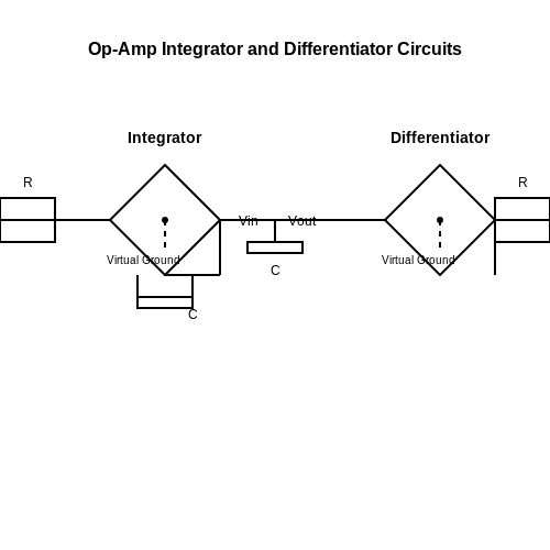
The op-amp integrator performs mathematical integration of the input signal, producing an output proportional to the integral of the input voltage. The circuit replaces the feedback resistor in an inverting amplifier with a capacitor, exploiting the current-voltage relationship in a capacitor:
Applying Kirchhoff's current law at the inverting input (virtual ground) gives:
Solving this differential equation yields the output voltage:
where Vout(0) represents the initial condition. In practical implementations, a large resistor is often placed in parallel with the feedback capacitor to prevent DC drift.
Frequency Response Analysis
The transfer function of an ideal integrator is:
This results in a constant -90° phase shift and a gain that decreases at 20 dB/decade. The integrator's unity-gain frequency occurs at:
Operational Amplifier as a Differentiator
The differentiator circuit produces an output proportional to the time derivative of the input signal. It swaps the positions of the resistor and capacitor from the integrator configuration:
The transfer function for an ideal differentiator is:
This produces a +90° phase shift and a gain increasing at 20 dB/decade. Practical differentiators require modifications to prevent high-frequency instability:
- A small capacitor in parallel with the input resistor limits high-frequency gain
- A resistor in series with the input capacitor reduces the circuit's Q-factor
Practical Considerations and Applications
Integrators find extensive use in:
- Analog computers for solving differential equations
- Waveform generation (triangular waves from square waves)
- PID controllers in the integral term implementation
Differentiators are employed in:
- Edge detection in pulse signals
- Frequency modulation circuits
- Rate-of-change measurements in control systems
Both circuits require careful compensation for real-world limitations. The integrator suffers from DC drift due to input bias currents and offset voltages, while the differentiator is prone to high-frequency noise amplification. Modern implementations often use active compensation techniques or switched-capacitor approaches to mitigate these issues.
Stability Analysis
The stability of these circuits depends on the op-amp's gain-bandwidth product and phase margin. For the integrator, the dominant pole introduced by the RC network generally improves stability. The differentiator, however, introduces a zero in the transfer function that can reduce phase margin. A stability analysis should consider:
where ωc is the crossover frequency and A(jω) is the op-amp's open-loop gain. Ensuring adequate phase margin (>45°) prevents oscillation in practical implementations.
3. Open-Loop Gain
3.1 Open-Loop Gain
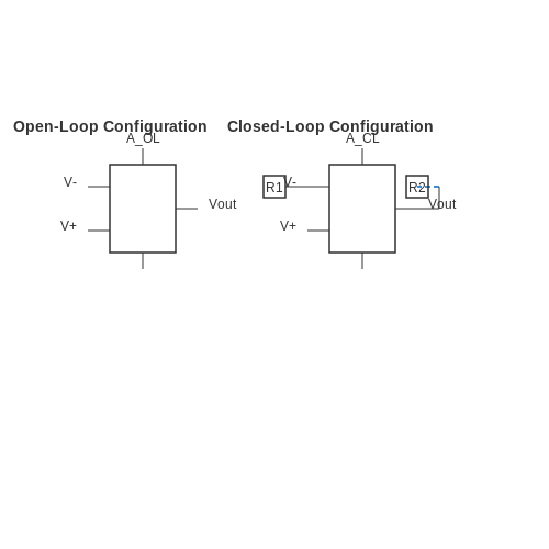
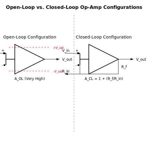
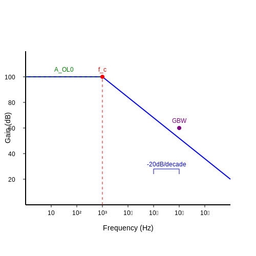
The open-loop gain (AOL) of an operational amplifier (op-amp) is the intrinsic voltage amplification achieved without any external feedback. In ideal conditions, AOL approaches infinity, but real-world op-amps exhibit finite gain due to semiconductor physics and design constraints. For precision applications, understanding the limitations imposed by finite AOL is critical.
Mathematical Definition
The open-loop gain is defined as the ratio of the output voltage (Vout) to the differential input voltage (Vdiff):
For a real op-amp, AOL is frequency-dependent and typically modeled as a first-order low-pass response:
where AOL0 is the DC open-loop gain, f is the operating frequency, and fc is the dominant-pole corner frequency.
Practical Implications
Finite AOL introduces errors in feedback configurations. For a non-inverting amplifier with feedback resistors R1 and R2, the closed-loop gain (ACL) deviates from the ideal value due to AOL:
where β is the feedback factor (β = R1 / (R1 + R2)). For AOLβ >> 1, this simplifies to 1/β, but at high frequencies or low AOL, the error becomes significant.
Frequency Response and Gain-Bandwidth Product
The gain-bandwidth product (GBW) is a key figure of merit, linking AOL and bandwidth:
For a voltage-feedback op-amp, GBW remains constant; doubling the closed-loop gain halves the usable bandwidth. This trade-off is critical in high-speed signal conditioning and filtering applications.
Measurement Techniques
Open-loop gain is measured using:
- DC sweep tests: Apply a small differential input and measure Vout.
- AC analysis: Use a network analyzer to plot AOL(f).
- SPICE simulation: Leverage op-amp macromodels with accurate AOL roll-off.
Case Study: Precision Instrumentation
In a 24-bit ADC driver circuit, a Texas Instruments OPA2205 (AOL0 = 140 dB) ensures < 1 LSB error at DC. However, at 10 kHz, AOL drops to 80 dB, necessitating bandwidth-aware design.
3.2 Input and Output Impedance
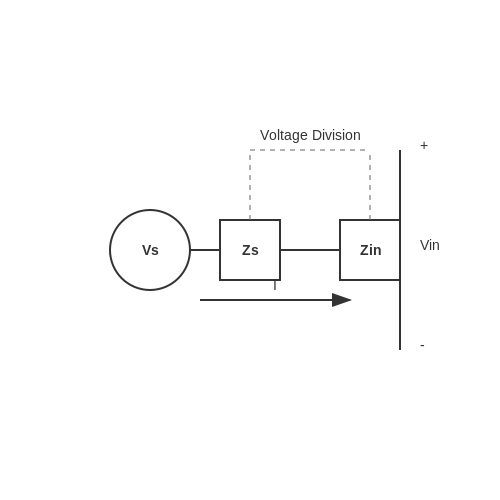
The input and output impedance of an operational amplifier (op-amp) are critical parameters that determine its interaction with external circuits. These impedances influence signal integrity, loading effects, and overall system performance.
Input Impedance
The input impedance of an op-amp defines how much it loads the preceding circuit. For an ideal op-amp, the input impedance is infinite, meaning no current flows into the input terminals. However, real op-amps exhibit finite input impedance, which varies depending on the configuration:
- Differential Input Impedance (Zid) — The impedance between the non-inverting and inverting inputs. For a bipolar junction transistor (BJT) input op-amp like the LM741, Zid is typically in the range of 2 MΩ to 6 MΩ.
- Common-Mode Input Impedance (Zicm) — The impedance from either input to ground. This is usually higher than Zid, often exceeding 100 MΩ for precision op-amps.
In a non-inverting amplifier configuration, the input impedance is significantly increased due to negative feedback:
where \( A_{ol} \) is the open-loop gain and \( \beta \) is the feedback factor.
Output Impedance
The output impedance (Zout) determines how much the op-amp's output voltage drops under load. An ideal op-amp has Zout = 0, but real op-amps exhibit a small but finite output impedance, typically in the range of 10 Ω to 100 Ω for general-purpose devices.
Negative feedback reduces the effective output impedance:
This equation highlights why closed-loop configurations (e.g., voltage followers) exhibit much lower output impedance than open-loop operation.
Practical Implications
Understanding input and output impedance is essential for:
- Impedance Matching — Ensuring minimal signal reflection and maximum power transfer between stages.
- Loading Effects — Preventing excessive current draw from high-impedance sources (e.g., sensors).
- Stability — Avoiding oscillations due to capacitive loading on high-output-impedance amplifiers.
For example, when driving a low-impedance load (e.g., a speaker), an additional buffer stage may be necessary to prevent signal degradation.
3.3 Bandwidth and Slew Rate
Bandwidth Limitations in Op-Amps
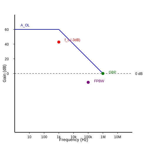
The open-loop gain (AOL) of an operational amplifier is frequency-dependent, exhibiting a first-order roll-off characteristic due to internal compensation. The gain-bandwidth product (GBP) defines the frequency at which the gain drops to unity (0 dB). For a dominant-pole compensated op-amp, the transfer function is:
where fc is the corner frequency. The GBP is constant, meaning:
In closed-loop configurations, bandwidth (f-3dB) scales inversely with gain:
Slew Rate: Large-Signal Dynamics
Slew rate (SR) quantifies the maximum rate of change of the output voltage, dictated by internal current limitations:
where Imax is the maximum available charging current and Ccomp is the compensation capacitance. For a sinusoidal input V(t) = V_p \sin(2\pi ft), the maximum slope occurs at the zero-crossing:
To avoid distortion, the slew rate must satisfy:
Full-Power Bandwidth
The full-power bandwidth (FPBW) is the frequency at which the op-amp's output reaches its maximum swing without slew-induced distortion:
For example, an op-amp with SR = 20 V/µs and Vmax = 10 V has FPBW ≈ 318 kHz.
Practical Implications
- High-speed applications (e.g., video amplifiers, ADCs) require op-amps with high GBP and SR.
- Trade-offs exist between bandwidth, noise, and power consumption.
- Compensation techniques (e.g., Miller compensation) stabilize amplifiers but reduce SR.
3.4 Common-Mode Rejection Ratio (CMRR)
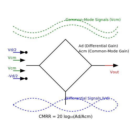
The Common-Mode Rejection Ratio (CMRR) quantifies an operational amplifier's ability to reject signals that appear simultaneously and in-phase on both inputs. This parameter is critical in applications where differential signals must be amplified while suppressing noise or interference common to both inputs, such as in instrumentation amplifiers, biomedical sensors, and communication systems.
Mathematical Definition
CMRR is defined as the ratio of the differential gain (Ad) to the common-mode gain (Acm):
Expressed logarithmically in decibels (dB):
For an ideal op-amp, Acm is zero, making CMRR infinite. In practice, mismatches in transistor pairs and resistor tolerances limit CMRR to finite values, typically ranging from 70 dB to over 120 dB in precision amplifiers.
Practical Derivation
Consider a non-inverting amplifier with a differential input signal Vd and a common-mode signal Vcm. The output voltage is:
To isolate CMRR, rewrite the equation in terms of the common-mode rejection ratio:
This shows that the effective error due to common-mode signals scales inversely with CMRR.
Factors Affecting CMRR
- Resistor Mismatch: In differential amplifiers, even slight mismatches in feedback resistors degrade CMRR. For a differential pair with resistor tolerances ΔR/R, CMRR is approximately:
- Transistor Mismatch: In the op-amp's input stage, variations in BJT or MOSFET parameters introduce common-mode gain.
- Power Supply Rejection: Poor power supply rejection (PSRR) can indirectly worsen CMRR if supply noise couples into the signal path.
Measurement Techniques
CMRR is measured by applying a common-mode signal and observing the output. A standard test setup involves:
- Configuring the op-amp in unity-gain mode.
- Applying a known common-mode voltage (Vcm).
- Measuring the output deviation (ΔVout).
The common-mode gain is then:
CMRR is calculated using the previously defined ratio.
Applications and Design Considerations
High CMRR is essential in:
- Instrumentation Amplifiers: Used in strain gauges and thermocouples where signals are small and noise is prevalent.
- Medical Electronics: ECG and EEG amplifiers must reject 50/60 Hz interference from power lines.
- Communication Systems: Differential signaling in twisted-pair cables relies on CMRR to suppress electromagnetic interference.
To maximize CMRR in designs:
- Use matched resistors (0.1% or better tolerance).
- Select op-amps with high intrinsic CMRR (>100 dB).
- Employ guard traces and shielding to minimize common-mode noise pickup.
4. Power Supply Requirements
4.1 Power Supply Requirements
Operational amplifiers require carefully designed power supply configurations to maintain proper functionality across their specified operating conditions. The power supply architecture directly impacts key performance parameters including output voltage swing, common-mode rejection ratio (CMRR), and total harmonic distortion (THD).
Single vs. Dual Supply Operation
Most operational amplifiers support both single-supply and dual-supply configurations, with the choice depending on application requirements:
- Dual-supply (±VCC): Provides symmetric voltage rails about ground, enabling bidirectional output swing. The total supply voltage VTOT = VCC+ - VCC- determines the maximum differential input range.
- Single-supply (VCC/GND): Requires input signals to remain above ground potential, with output limited to the range VOL to VCC - VOH.
where VSAT represents the output saturation voltage, typically 1-2V below rail for modern amplifiers.
Power Supply Rejection Ratio (PSRR)
The PSRR quantifies an op-amp's ability to reject power supply variations from appearing at the output:
High-performance amplifiers achieve PSRR > 100 dB at DC, degrading at higher frequencies due to limited internal compensation. The PSRR curve typically shows a pole-zero structure related to the amplifier's internal biasing networks.
Current Consumption and Thermal Considerations
The total supply current IQ consists of quiescent current and load current:
Junction temperature rise must be calculated using the thermal impedance θJA:
where TA is ambient temperature and θJA is package-dependent (typically 50-150°C/W for SOIC packages).
Decoupling and Stability
Proper power supply decoupling is critical for maintaining stability and preventing oscillation:
- Place 0.1 μF ceramic capacitors within 5 mm of each supply pin
- Add bulk capacitance (10-100 μF) for systems with dynamic loads
- Use separate feedthrough inductors for sensitive analog stages
The impedance of the power delivery network should satisfy:
across the entire frequency range of operation.
Modern Low-Voltage Design Challenges
With supply voltages decreasing to 1.8V or lower in modern systems, several considerations emerge:
- Input common-mode range must include both supply rails (rail-to-rail input)
- Output stages require complementary folded-cascode topologies for rail-to-rail swing
- Increased sensitivity to ground bounce and supply noise
The minimum usable supply voltage VMIN is determined by:
where VGS is the gate-source voltage, VDSAT the saturation voltage, and VMARGIN accounts for process variations.
4.2 Offset Voltage and Bias Current
Input Offset Voltage
The input offset voltage (VOS) is a critical non-ideal characteristic of operational amplifiers, defined as the differential DC voltage required between the inputs to force the output to zero. In an ideal op-amp, VOS would be zero, but manufacturing mismatches in the input differential pair introduce this error. For precision applications, VOS can introduce significant DC errors, especially in high-gain configurations.
where Rf is the feedback resistor and Rin is the input resistor. Bipolar and CMOS op-amps exhibit different typical offset ranges, with precision amplifiers offering VOS as low as 1 µV.
Input Bias Current
Input bias current (IB) arises from the finite base or gate current required by the input transistors. Bipolar op-amps exhibit higher bias currents (nA to µA) due to base current requirements, while CMOS op-amps have fA to pA levels. The bias current flows through external impedances, generating offset voltages:
where Req is the equivalent resistance seen by the input. To minimize this effect, match the impedances at both inputs.
Input Offset Current
The input offset current (IOS) is the difference between the two bias currents (IB+ − IB−). Even with matched impedances, IOS introduces an error:
Compensation Techniques
Several methods mitigate offset and bias effects:
- External Nulling: Use a potentiometer to inject a compensating voltage at the offset null pins.
- Chopper Stabilization: Dynamically corrects offset via auto-zeroing techniques, reducing drift.
- Impedance Balancing: Matching resistances at both inputs minimizes bias-induced offsets.
Practical Implications
In instrumentation amplifiers, uncorrected offset voltages can saturate the output or introduce measurement errors. For example, a 1 mV offset in a medical ECG amplifier with 1000x gain produces a 1 V error, masking critical signals. Low-offset amplifiers like the OPA333 or LTC2050 are preferred for such applications.
Temperature Drift
Offset voltage and bias current vary with temperature, quantified by:
where TCVOS is the temperature coefficient (µV/°C). Precision amplifiers specify drift to ensure stability across operating conditions.
4.3 Stability and Compensation Techniques
Open-Loop Gain and Phase Margin
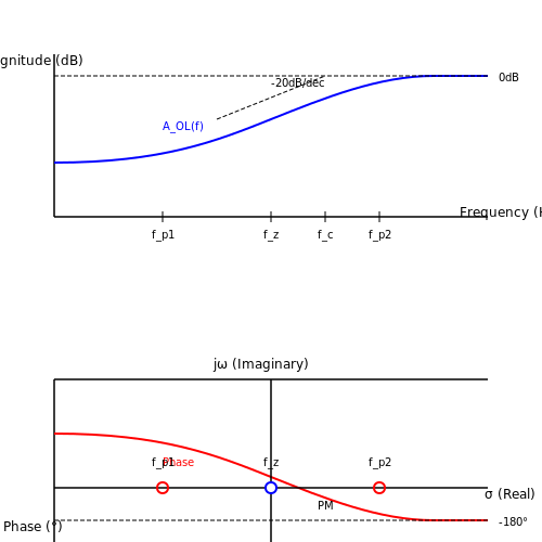
Stability in operational amplifiers is determined by the open-loop gain and phase response. The open-loop gain AOL rolls off with frequency due to internal poles, typically following a first-order response:
where A0 is the DC gain and fp1 is the dominant pole frequency. Phase margin (PM) is a critical metric for stability, defined as:
where fc is the crossover frequency (where |AOL| = 1). A phase margin below 45° leads to excessive ringing or oscillation, while >60° ensures a well-damped response.
Pole Splitting and Miller Compensation
Many op-amps use Miller compensation to stabilize the amplifier by introducing a dominant pole. A compensation capacitor CC is placed across a high-gain stage, effectively splitting the poles:
Here, gm2 is the transconductance of the second stage, R1 and R2 are resistances at the first and second stages, and CL is the load capacitance. This technique pushes the non-dominant pole to higher frequencies, improving phase margin.
Lead-Lag Compensation
For amplifiers with multiple poles, lead-lag compensation introduces a zero to counteract phase lag. The transfer function modifies to:
where τz and τp are the time constants of the zero and pole, respectively. Proper placement of the zero (fz < fp2) can extend the phase margin without sacrificing bandwidth.
Practical Compensation Techniques
- Dominant-Pole Compensation: Reduces bandwidth but ensures stability by rolling off gain before secondary poles affect phase.
- Feedforward Compensation: Bypasses high-frequency signals around slow stages to reduce phase lag.
- Output-Stage Compensation: Uses small capacitors at the output to suppress high-frequency oscillations.
In high-speed amplifiers, current-feedback architectures often employ resistive compensation to maintain stability across varying gains.
Stability in Feedback Networks
The feedback network's phase contribution must be considered. For resistive feedback, stability is primarily governed by the op-amp's internal dynamics. However, capacitive feedback introduces additional poles:
If fp,FB is too close to the amplifier's crossover frequency, instability may arise. A common solution is to add a small feedback capacitor Cf to introduce phase lead:
This ensures the zero cancels the feedback pole, preserving phase margin.
4.4 Noise and Thermal Considerations
Noise Sources in Operational Amplifiers
Operational amplifiers exhibit several intrinsic noise mechanisms, primarily categorized as thermal noise, flicker noise (1/f noise), and shot noise. Thermal noise arises from the random motion of charge carriers in resistive elements and is described by the Nyquist relation:
where k is Boltzmann's constant (1.38 × 10⁻²³ J/K), T is the absolute temperature, R is the resistance, and B is the bandwidth. Flicker noise, dominant at low frequencies, follows an inverse frequency dependence:
where Kf is a device-specific constant. Shot noise, prevalent in semiconductor junctions, is given by:
where q is the electron charge (1.6 × 10⁻¹⁹ C) and IDC is the DC current.
Equivalent Input Noise Model
The total noise of an op-amp is often modeled as a combination of voltage and current noise sources at the input. The equivalent input noise voltage density (en) and current density (in) are specified in datasheets. The total output noise is computed by integrating these contributions over the bandwidth:
where Rs is the source resistance. For wideband applications, the noise bandwidth must account for the filter roll-off.
Thermal Effects and Drift
Temperature variations introduce offset voltage drift (dVos/dT) and bias current drift (dIb/dT), typically specified in µV/°C and nA/°C, respectively. These drifts are critical in precision applications, such as instrumentation amplifiers or medical devices. The thermal resistance (θJA) of the package determines the junction temperature rise:
where Ta is the ambient temperature and Pd is the power dissipation.
Minimizing Noise and Thermal Drift
- Component Selection: Choose op-amps with low en and in for sensitive applications (e.g., LT1028, AD797).
- Bandwidth Limiting: Use filters to restrict noise bandwidth to the signal's useful range.
- Thermal Management: Employ heat sinks or low-θJA packages to stabilize temperature.
- Balanced Layouts: Symmetric PCB traces reduce thermocouple effects and EMI pickup.
Case Study: Low-Noise Photodiode Amplifier
In a transimpedance amplifier for photodiodes, the feedback resistor (Rf) dominates thermal noise. For a 1 MΩ resistor at 300 K and 10 kHz bandwidth:
Using a lower Rf or cooling the circuit reduces noise. Parallel amplifiers or chopper stabilization may further mitigate flicker noise.
5. Negative Feedback and Stability
5.1 Negative Feedback and Stability
Negative feedback is a fundamental mechanism in operational amplifier (op-amp) circuits that ensures stability, linearity, and predictable behavior. By feeding a portion of the output signal back to the inverting input, the system counteracts deviations from the desired operating point, reducing gain sensitivity to component variations and nonlinearities.
Feedback Network Analysis
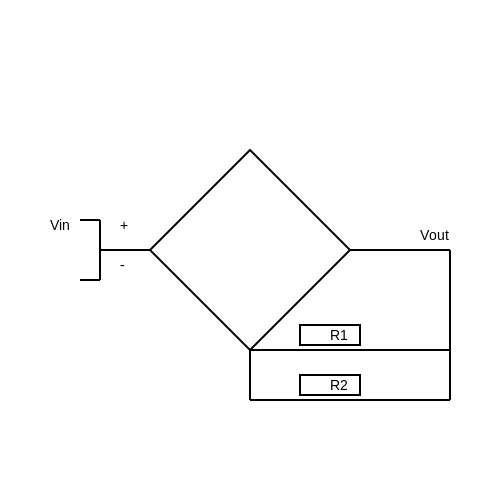
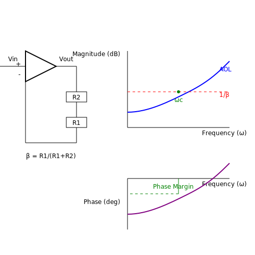
Consider a basic non-inverting amplifier configuration, where the output voltage Vout is fed back to the inverting input through a resistive divider network R1 and R2. The feedback factor β is defined as:
The closed-loop gain ACL of the system is then derived from the open-loop gain AOL and feedback factor:
For large open-loop gains (AOLβ ≫ 1), this simplifies to:
Stability Criteria and Phase Margin
Stability in feedback systems is governed by the Barkhausen stability criterion, which states that oscillations occur if the loop gain AOLβ satisfies:
To ensure stability, the phase margin—the difference between the loop gain phase shift and 180° at the frequency where |AOLβ| = 1—must be positive. A phase margin of 45° or more is typically required to avoid excessive ringing and overshoot in transient responses.
Frequency Compensation Techniques
Many op-amps incorporate internal frequency compensation to ensure stability under various feedback conditions. Dominant-pole compensation introduces a low-frequency pole that rolls off the gain at -20 dB/decade, preventing the loop gain from reaching unity before excessive phase shift occurs.
External compensation techniques include:
- Miller Compensation: A capacitor placed across a high-gain stage to introduce a dominant pole.
- Lead-Lag Compensation: A combination of resistors and capacitors to adjust phase response.
- Input Filtering: Reducing high-frequency feedback signals that could induce instability.
Practical Implications
In real-world applications, parasitic capacitances and inductances can introduce unintended phase shifts, potentially destabilizing the circuit. Careful PCB layout, proper grounding, and judicious selection of feedback components are critical to maintaining stability. For instance, stray capacitance across R2 in a feedback network can create an unintended high-frequency pole, degrading phase margin.
Modern op-amps often include built-in compensation for unity-gain stability, but higher-performance designs may require external compensation tailored to specific closed-loop gain requirements.
Mathematical Derivation of Stability Conditions
Analyzing the transfer function of a feedback system reveals stability constraints. Consider a generic second-order system:
where ωp1 and ωp2 are pole frequencies. The loop gain is:
The phase shift at frequency ω is:
For stability, the phase margin PM must satisfy:
where ωc is the crossover frequency where |L(jωc)| = 1.
5.2 Active Filters Using Op-Amps
Active filters leverage operational amplifiers to achieve frequency-selective responses without relying on passive components alone. Unlike passive LC filters, active designs avoid bulky inductors, offering compactness, precise tuning, and impedance isolation. The op-amp's high input impedance and low output impedance enable cascading stages without loading effects, while feedback networks define filter characteristics.
First-Order Active Filters
The simplest active filter is a first-order low-pass or high-pass configuration. For a low-pass filter, a resistor-capacitor (RC) network feeds into the op-amp's inverting input, with the transfer function given by:
Here, Rf sets the DC gain, while the pole frequency fp = 1/(2πRfC) determines the cutoff. A high-pass variant swaps the resistor and capacitor positions, yielding:
Second-Order Sallen-Key Topology
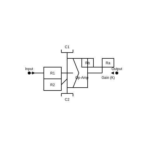
Butterworth, Chebyshev, or Bessel responses require at least second-order stages. The Sallen-Key architecture, a non-inverting configuration, uses two RC pairs and a gain-setting network. For a low-pass filter:
where K = 1 + Rb/Ra is the passband gain. The quality factor Q and cutoff frequency ω0 are:
State-Variable Filters
For independently tunable parameters, state-variable filters employ multiple op-amps to separate low-pass, high-pass, and band-pass outputs. A typical implementation uses three integrators and a summing amplifier:
This topology allows precise control over Q (via R3) and ω0 (via R1, R2, C1, C2), making it ideal for parametric equalizers.
Practical Considerations
- Op-amp bandwidth must exceed the filter's cutoff frequency to avoid phase margin degradation.
- Component tolerances affect Q and f0; 1% resistors and NP0 capacitors are recommended for critical applications.
- Noise gain peaks near the cutoff in high-Q designs, necessitating low-noise op-amps.
5.3 Precision Rectifiers
Standard diode rectifiers suffer from a forward voltage drop (VF), typically 0.7 V for silicon diodes, which introduces significant error in low-voltage signal processing. Precision rectifiers leverage operational amplifiers to eliminate this nonlinearity, enabling accurate AC-to-DC conversion even for signals in the millivolt range.
Half-Wave Precision Rectifier
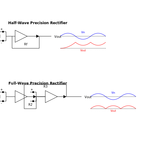
The simplest form consists of an op-amp configured as an inverting amplifier with a diode in the feedback path. When the input signal Vin is positive, the op-amp output goes negative, reverse-biasing the diode and forcing the output to zero. For negative inputs, the op-amp drives the diode into conduction, producing a positive output:
The op-amp's high open-loop gain compensates for the diode's forward voltage, reducing the effective dead zone to microvolts. Practical implementations often include a second diode to prevent saturation during positive half-cycles.
Full-Wave Precision Rectifier (Absolute Value Circuit)
A more advanced configuration combines two op-amp stages to rectify both half-cycles. The first stage operates as an inverting half-wave rectifier, while the second stage sums the original input and the rectified signal with appropriate weighting:
By setting R1 = R2 = 2R3, the circuit achieves perfect full-wave rectification:
Nonidealities and Compensation
Key limitations include:
- Bandwidth constraints: Slew rate and gain-bandwidth product limit high-frequency performance
- Phase reversal: Some op-amps exhibit output phase inversion when inputs exceed common-mode range
- DC offsets: Input bias currents generate small output errors
Modern solutions employ:
- JFET-input op-amps for low bias currents
- Active compensation networks to cancel offsets
- High-speed amplifiers for RF applications
Applications in Measurement Systems
Precision rectifiers serve critical roles in:
- True RMS converters for AC power measurement
- Envelope detection in communication receivers
- Peak-hold circuits for transient analysis
- Analog computing modules for nonlinear operations
In instrumentation applications, the AD824 and OPA2182 families provide sub-millivolt accuracy with bandwidths exceeding 10 MHz, enabling rectification of signals up to several hundred kilohertz.
5.4 Instrumentation Amplifiers
Instrumentation amplifiers (IAs) are precision differential amplifiers optimized for high common-mode rejection ratio (CMRR), low noise, and high input impedance. Unlike standard operational amplifiers, IAs are designed to amplify small differential signals in the presence of large common-mode voltages, making them indispensable in biomedical sensors, strain gauges, and industrial measurement systems.
Architecture and Key Features
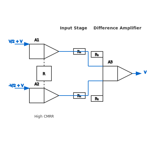
The classic three-op-amp instrumentation amplifier consists of two non-inverting input stages followed by a difference amplifier. The input stage provides high impedance and gain, while the output stage rejects common-mode signals. The differential gain Ad is set by a single resistor RG:
where R1 is the matched feedback resistor of the input stage. The CMRR is determined by the ratio matching of resistors in the difference amplifier, typically exceeding 100 dB in precision ICs like the AD620 or INA128.
Mathematical Derivation of CMRR
For a differential input Vd and common-mode input Vcm, the output is:
where Acm is the common-mode gain. The CMRR in decibels is derived as:
Mismatches in resistor ratios R2/R3 of the difference amplifier introduce common-mode errors. For a 0.1% mismatch, CMRR degrades to approximately 66 dB.
Practical Design Considerations
- Input Bias Currents: FET-input op-amps reduce errors in high-impedance sensor interfaces.
- Noise Performance: Voltage noise density (e.g., 3 nV/√Hz in the INA333) must be weighed against bandwidth requirements.
- Gain Nonlinearity: Monolithic IAs maintain <0.01% nonlinearity through laser-trimmed resistors.
Applications in Measurement Systems
In ECG amplifiers, IAs reject 50/60 Hz interference from power lines while amplifying microvolt-level cardiac signals. Load cells in weighbridges use IAs to compensate for long cable runs introducing common-mode noise. Modern integrated IAs (e.g., AD8421) incorporate EMI filtering and rail-to-rail outputs for industrial environments.
6. Recommended Textbooks
6.1 Recommended Textbooks
- PDF Franco-3930368 fra28167˙fm December 11, 2013 16:50 — Franco-3930368 fra28167˙fm December 11, 2013 16:50 CONTENTS Preface xi 1 Operational Amplifier Fundamentals 1 1.1 Amplifier Fundamentals 3 1.2 The Operational Amplifier 6 1.3 Basic Op Amp Configurations 9 1.4 Ideal Op Amp Circuit Analysis 16 1.5 Negative Feedback 24 1.6 Feedback in Op Amp Circuits 30 1.7 The Return Ratio and Blackman's Formula 38 1.8 Op Amp Powering 46
- PDF INTRODUCTION TO CMOS OP-AMPS AND COMPARATORS - Wiley — 4.5 Dynamic Range of CMOS Op-Amps / 126 4.6 Frequency Response, Transient Response, and Slew Rate of Compensated CMOS Op-Amps / 132 4.7 Noise Performance of CMOS Op-Amps / 137 4.8 Fully Differential Op-Amps / 140 4.9 CMOS Output Stages / 149 4.10 Op-Amps with Rail-to-Rail Input Common-Mode Range / 164 Problems / 170 References / 173 5 ...
- CHAPTER 6: The Operational Amplifier - Introduction to Electric ... — 6.8 Analysis of Op Amp Circuits Using MATLAB. 6.9 Using PSpice to Analyze Op Amp Circuits. 6.10 How Can We Check … ? 6.11 DESIGN EXAMPLE—Transducer Interface Circuit. 6.12 Summary. Problems. PSpice Problems. Design Problems. 6.1 Introduction. This chapter introduces another circuit element, the operational amplifier, or op amp.
- PDF Operational Amplifiers - Learn About Electronics — good news is that the op amp does! Amplifiers Module 6 What you'll learn in Module 6. Section 6.0. Introduction to Operational Amplifiers. Understand Concept of the Ideal Amplifier and the Need for Integrated Circuits. Section 6.1 Op Amp Inputs. •Typical op amp input requirements. Section 6.2 Comparators. • Open Loop Mode, The Schmitt ...
- PDF Op Amps for Everyone Design Guide (Rev. B) - MIT — feedback op amp equations, and they teach the concept of relative stability and com-pensation of potentially unstable op amps. Chapter 8 develops the current feedback op amp equations and discusses current feedback stability. Chapter 9 compares current feedback and voltage feedback op amps. The meat of this book is Chapters 12, 13, and
- PDF Fundamentals of Electronic Circuit Design - University of Cambridge — 8.1 Op amp Basics 8.2 Op amp circuits 8.2.1 non-inverting amplifier 8.2.2 inverting amplifier 8.2.3 signal offset 9 Filters 9.1 The Decibel Scale 9.2 Single-pole Passive Filters 9.3 Metrics for Filter Design 9.4 Two-pole Passive Filters 9.5 Active Filters 9.5.1 First order low pass 9.5.2 First order high pass 9.5.3 Second order low pass
- 6.1: Introduction to Specialized Op Amps - Engineering LibreTexts — There are a variety of other useful variations on the basic op amp theme. These include devices optimized for single-supply operation, dedicated voltage followers, devices that allow you to trade off speed for power consumption, and application-specific items like low-noise audio pre-amplifiers and voltage-controlled amplifiers.
- Chapter 6. Operational Amplifiers - Applied Electrical ... - UMass — 2.1 Basic Physics Review; 2.2 First Circuit; 2.3 Circuit Elements; 2.4 Current and Voltage Sources; 2.5 AC and DC waveforms, average and RMS values; ... The op amp is an active electronic device constructed from dozens of transistors; the details of such construction are not of concern to us here. Instead, our interest is in using op amps for ...
- Operational Amplifiers & Linear Integrated Circuits: Theory and ... — The goal of this text, as its name implies, is to allow the reader to become proficient in the analysis and design of circuits utilizing modern linear ICs. It progresses from the fundamental circuit building blocks through to analog/digital conversion systems. The text is intended for use in a second year Operational Amplifiers course at the Associate level, or for a junior level course at the ...
- Operational amplifiers | Basic Electronics for Scientists and Engineers ... — Discover Basic Electronics for Scientists and Engineers, 1st Edition, Dennis L. Eggleston on Higher Education from Cambridge
6.2 Online Resources and Datasheets
- 64 Basic Op-Amp Circuits - Forum for Electronics — A is the open loop gain of the op-amp. The circuit symbol for an op-amp is shown in Figure 6.1. The pin connections for the 8 pin DIP package µA741 op-amp are given in Figure 6.2. Chip Diagrams: Vcc+ uA 741 6 OUT IN-8-7 + 2 IN+ Vcc-34 5 1 IN+ _ OUT + IN-Vcc+ Vcc-Figure 6.1 Symbol for a basic op-amp Figure 6.2 The µA741 op-amp package.
- PDF Operational Amplifiers - Learn About Electronics — good news is that the op amp does! Amplifiers Module 6 What you'll learn in Module 6. Section 6.0. Introduction to Operational Amplifiers. Understand Concept of the Ideal Amplifier and the Need for Integrated Circuits. Section 6.1 Op Amp Inputs. •Typical op amp input requirements. Section 6.2 Comparators. • Open Loop Mode, The Schmitt ...
- Introduction to Op amps - Learn About Electronics — Understand Concept of the Ideal Amplifier and the Need for Integrated Circuits. Section 6.1 Op Amp Inputs. •Typical op amp input requirements. Section 6.2 Comparators. • Open Loop Mode, The Schmitt Trigger. • Hysteresis & Positive Feedback. Section 6.3 Voltage Amplifiers. • The ideal op amp, NFB, Op amp rules.
- PDF CHAPTER 1: THE OP AMP - Analog — determines the quality of the op amp. This is referred to as the voltage feedback model. This type of op amp comprises nearly all op amps below 10 MHz bandwidth and on the order of 90% of those with higher bandwidths. Figure 1.2: The Attributes of an Ideal Op Amp Basic Operation The basic operation of the op amp can be easily summarized.
- PDF Basic OpAmp Design and Compensation - University of Minnesota Duluth — Basic OpAmp Design and Compensation Chapter 6 . Chapter 6 Figure 01 6.1 OpAmp applications Typical applications of OpAmps in analog integrated circuits: ... is a common-source amplifier. Shown in the diagram are reasonable widths in 0.18um technology (length all made 0.3um). Reasonable sizes for the lengths are usually 1.5 to 10 times of the
- PDF OPERATIONAL AMPLIFIERS: Basic Circuits and Applications - Texas A&M ... — - The Operational Amplifier (op amp) was invented in the 40's. Bell Labs filed a patent in 1941 and many consider the first practical op amp to be the vacuum tube K2-W invented in 1952 by George Philbrick. - Texas Instruments invented the integrated circuit in 1958 which paved the way for Bob Widlar at Fairchild inventing the uA702 solid state
- Chapter 6. Operational Amplifiers - Applied Electrical ... - UMass — The schematic symbol for the op amp is a triangle having two inputs and one output. Figure 6.1 Op amp schematic symbol. The op amp is an active electronic device constructed from dozens of transistors; the details of such construction are not of concern to us here.
- PDF Operational amplifiers - University of Washington — Datasheets sometimes use these phrases to describe open-loop voltage gain: large-signal voltage gain, differential voltage gain, open-loop frequency response, etc. 5.1.5 Slew rate When a large signal (e.g. a step signal of 20Vpp) is applied to the input of the opamp quickly, the opamp cannot respond fast enough to follow the input signal.
- Operational Amplifier Basics - Op-amp tutorial — The circuit operates from a dual supply +Vcc and -Vee which ensures a constant supply. The voltage that appears at the output, Vout of the amplifier is the difference between the two input signals as the two base inputs are in anti-phase with each other. So as the forward bias of transistor, TR1 is increased, the forward bias of transistor TR2 is reduced and vice versa.
- Operational Amplifiers - Learn About Electronics - studylib.net — The Op Amp as a Comparator Basic op amp types such as the 741 will perform adequately as comparators in simple circuits, such as a temperature controlled switch that is required to switch on or off a circuit when the input voltage from a temperature sensor is higher or lower than a preset reference value. ... See the LMC660 datasheet from Texas ...
6.3 Research Papers and Application Notes
- Operational Amplifiers - Learn About Electronics - studylib.net — Module 6 Amplifiers Operational Amplifiers The Ideal Amplifier What you'll learn in Module 6. Section 6.0. Introduction to Operational Amplifiers. Understand Concept of the Ideal Amplifier and the Need for Integrated Circuits. Section 6.1 Op Amp Inputs. •Typical op amp input requirements. Section 6.2 Comparators. • Open Loop Mode, The Schmitt Trigger. • Hysteresis & Positive ...
- PDF Operational Amplifiers - Learn About Electronics — What you'll learn in Module 6. Section 6.0. Introduction to Operational Amplifiers. Understand Concept of the Ideal Amplifier and the Need for Integrated Circuits. Section 6.1 Op Amp Inputs. ••Typical op amp input requirements. Section 6.2 Comparators. • Open Loop Mode, The Schmitt Trigger.
- Chapter 6. Operational Amplifiers - Applied Electrical Engineering ... — Chapter 6. Operational Amplifiers The operational amplifier, or op amp, is an active electronic device used for many applications including signal amplification, filtering, comparing voltage values, adding signals together, buffering, or isolating components of a circuit, and creating timing oscillators. Op amps are active devices, meaning that power needs to be supplied to them, in the form ...
- PDF OP-AMP Basics - University of Nevada, Las Vegas — OP-AMP Basics Operational amplifiers are convenient building blocks that can be used to build amplifiers, filters, and even an analog computer. Op-amps are integrated circuits composed of many transistors & resistors such that the resulting circuit follows a certain set of rules. The most common type of op-amp is the voltage feedback type and that's what we'll use.
- PDF ENEE 611: Background Electronics Analysis and Design Laboratory - UMD — This part of your lab is to provide a review of op-amps, and to give you an opportunity to use the power supply circuit you made in a real application. Recall that an op-amp is a three- terminal integrated circuit. Inside the op-amp is a fairly complicated circuit which typically consists of more than thirty transistors.
- Chapter 6 Op-Amp - Springer — A typical op-amp, shown in Fig. 6.1, is an integrated device with a non-inverting input, an inverting input, two DC power supply leads (positive and negative), an output terminal, and a few other specialized leads used for ne-tuning (Figs. 6.2 and 6.3).
- Operational Amplifiers: Basic Concepts - Academia.edu — AI-generated Abstract The paper discusses the fundamental characteristics and historical development of operational amplifiers (Op-Amps). Key properties such as infinite input impedance, zero output impedance, and the concept of gain are highlighted, alongside a brief history of significant milestones in Op-Amp design.
- Op Amps - lecture notes with proper explanations - Studocu — normally built in a single integrated circuit (I.) and are used as the basic building block for many applications mostly as high gain d. and a. voltage amplifiers. Analysis of circuits containing op-amps is usually simplified by assuming that the device is ideal. The power supply is normally a dual balanced d. supply in the range Vs = 5V to 15V.
- (PDF) Operational Amplifiers - Academia.edu — This chapter also presents macromodels and measurement techniques for OpAmp parameters. A systematic treatment of sources of errors in important applications of the above four basic types of operational amplifiers is presented in Chap. 3. Input stages are evaluated in Chap. 4.
- Operational Amplifiers & Linear Integrated Circuits: Theory and ... — The goal of this text, as its name implies, is to allow the reader to become proficient in the analysis and design of circuits utilizing modern linear ICs. It progresses from the fundamental circuit building blocks through to analog/digital conversion systems. The text is intended for use in a second year Operational Amplifiers course at the Associate level, or for a junior level course at the ...