High-Voltage Differential Probes
1. Definition and Purpose of Differential Probes
Definition and Purpose of Differential Probes
A high-voltage differential probe is an instrument designed to measure voltage differences between two points in a circuit where neither point is referenced to ground. Unlike single-ended probes, which measure voltage relative to a common ground, differential probes isolate and amplify the potential difference between two floating signals, rejecting common-mode noise in the process.
Core Operating Principle
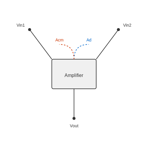
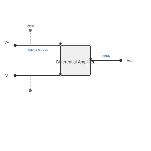
The fundamental operation of a differential probe relies on a precision differential amplifier with high common-mode rejection ratio (CMRR). The probe measures the voltage difference Vdiff between its two inputs (V+ and V−), while attenuating any common-mode voltage Vcm present on both inputs. The output voltage Vout is given by:
where Ad is the differential gain and Acm is the common-mode gain. The CMRR, expressed in decibels, quantifies the probe's ability to reject common-mode signals:
Key Design Parameters
High-voltage differential probes are characterized by several critical specifications:
- Bandwidth: The frequency range over which the probe maintains accurate measurements, typically from DC to several hundred MHz.
- Input Voltage Range: The maximum differential and common-mode voltages the probe can handle without saturation or damage, often exceeding ±1000 V.
- Input Impedance: High input resistance (e.g., 1 MΩ or more) and low capacitance (e.g., <1 pF) to minimize circuit loading.
- Attenuation Ratio: Fixed or selectable scaling (e.g., 100:1, 500:1) to adapt to varying signal amplitudes.
Practical Applications
Differential probes are indispensable in scenarios where ground reference is impractical or dangerous, such as:
- Measuring switching waveforms in half-bridge or full-bridge power converters.
- Analyzing signals in floating systems, like motor drives or isolated communication lines.
- High-voltage environments, including power electronics, CRT displays, or pulsed systems.
Historical Context
The development of differential probes paralleled advancements in high-speed oscilloscopes and power electronics. Early designs in the 1960s used transformer-based isolation, while modern probes employ high-voltage op-amps or specialized integrated circuits (e.g., difference amplifiers) for improved accuracy and bandwidth.
Mathematical Derivation: Noise Rejection
Consider a differential probe with inputs V+ = Vsig + Vnoise and V− = −Vsig + Vnoise. The differential and common-mode voltages are:
The output voltage becomes:
For a high CMRR (e.g., 60 dB), Acm ≈ Ad/1000, effectively suppressing noise by a factor of 1000.
Key Specifications and Performance Metrics
Bandwidth and Rise Time
The bandwidth of a high-voltage differential probe defines the frequency range over which the probe can accurately measure signals without significant attenuation. For a probe with a first-order frequency response, the -3 dB bandwidth (fBW) is related to the rise time (tr) by:
For example, a 100 MHz probe typically exhibits a rise time of 3.5 ns. In practice, the actual rise time may be slightly longer due to higher-order system dynamics. Bandwidth limitations arise from the probe's internal compensation networks and the parasitic capacitance of its input stage.
Common-Mode Rejection Ratio (CMRR)
CMRR quantifies a probe's ability to reject signals common to both inputs while amplifying the differential signal. Expressed in decibels, it is given by:
where Ad is the differential gain and Ac is the common-mode gain. High-quality probes achieve CMRR values exceeding 60 dB at DC, though this degrades with frequency due to asymmetries in the probe's input stage. For instance, a 1% mismatch in input capacitance can reduce CMRR to 40 dB at 10 MHz.
Input Impedance and Loading Effects
The input impedance (Zin) of a differential probe consists of resistive and capacitive components:
Typical values range from 1 MΩ to 10 MΩ in parallel with 1 pF to 10 pF. High input resistance minimizes DC loading, while low capacitance preserves signal integrity at high frequencies. However, the distributed nature of real-world circuits means that even small capacitances can form unintended voltage dividers with source impedances.
Voltage Range and Overload Protection
Differential probes specify both differential and common-mode voltage limits. The differential range (e.g., ±1000 V) determines the maximum potential difference between inputs, while the common-mode range (e.g., ±2000 V to ground) defines the absolute voltage tolerance. Protection circuits often incorporate gas discharge tubes and transient voltage suppressors to withstand fast transients exceeding these ratings.
Noise and Sensitivity
The noise floor, typically specified in mV/√Hz or μVRMS, determines the smallest detectable signal. For a probe with 10 nV/√Hz input noise and 1 GHz bandwidth, the total integrated noise is:
This fundamentally limits the measurement of small signals superimposed on high-voltage waveforms, such as ripple in power converters.
Propagation Delay and Phase Matching
Differential probes introduce propagation delays (typically 5-50 ns) due to signal conditioning electronics. For accurate timing measurements, the delay mismatch between channels must be less than 1% of the signal's rise time. High-end probes achieve phase matching within ±1° up to the probe's bandwidth limit.
Temperature Coefficients
Critical parameters like gain and offset vary with temperature. A probe might specify:
- Gain drift: ±0.01%/°C
- Offset drift: ±100 μV/°C
These become significant when measuring DC or low-frequency signals in environments with >10°C temperature fluctuations.
Calibration and Long-Term Stability
High-voltage probes require periodic calibration due to dielectric absorption in insulation materials and aging of precision resistors. Metrology-grade probes maintain ±0.5% accuracy for 12 months, while general-purpose models may drift by ±3% per year. Automated calibration systems often use Kelvin-Varley dividers to verify high-voltage scaling ratios.
1.3 Comparison with Single-Ended Probes
Measurement Principle and Signal Referencing
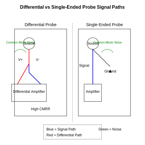
Single-ended probes measure a signal with respect to a common ground reference, typically the earth ground of the oscilloscope. This introduces a critical limitation: any ground loop currents or common-mode noise directly corrupts the measurement. In contrast, differential probes measure the potential difference between two points, neither of which needs to be ground-referenced. The output voltage Vout of a differential probe is given by:
where Ad is the differential gain and Ac is the common-mode gain. The common-mode rejection ratio (CMRR), defined as 20 log10(Ad/Ac), quantifies the probe's ability to reject ground-referenced noise.
Noise Immunity and Ground Loops
Single-ended probes are susceptible to ground loops when measuring high-frequency or high-current circuits. The probe's ground lead inductance forms a resonant tank circuit with parasitic capacitances, leading to ringing and measurement artifacts. Differential probes eliminate this issue by:
- Isolating the measurement from ground loops
- Rejecting common-mode noise through balanced signal paths
- Maintaining consistent impedance matching
For a single-ended probe with 10 nH of ground lead inductance, the resonant frequency fres with 5 pF of stray capacitance is:
Voltage Range and Floating Measurements
Single-ended probes are limited by the oscilloscope's maximum input voltage (typically ±40V for 1MΩ inputs). Differential probes use specialized attenuators and isolation to handle kilovolt-level signals. The breakdown voltage VBD of a differential probe's isolation barrier follows:
where Edielectric is the dielectric strength, d is the separation distance, and εr is the relative permittivity. High-voltage differential probes often use ceramic or polyimide insulation with Edielectric > 20 kV/mm.
Bandwidth and Signal Fidelity
Differential probes maintain higher bandwidth fidelity due to their symmetric construction. The frequency response H(f) of a properly matched differential probe is:
where f3dB is the -3dB point. Single-ended probes exhibit asymmetric roll-off due to ground lead effects, typically losing 3-6 dB of bandwidth when the ground lead length approaches λ/10 of the measured signal.
Practical Applications and Trade-offs
In power electronics measurements, differential probes enable accurate switching loss analysis in half-bridge configurations where neither switch node is ground-referenced. The table below summarizes key comparison metrics:
| Parameter | Single-Ended Probe | Differential Probe |
|---|---|---|
| Maximum Voltage | ±40V (typical) | ±6kV (high-end) |
| CMRR @ 1MHz | 0-20 dB | 60-100 dB |
| Bandwidth | 500 MHz (with artifacts) | 1 GHz (clean) |
| Ground Reference | Required | Not required |
When measuring high-speed serial data links (PCIe, USB 3.0), differential probes provide superior eye diagram clarity by rejecting common-mode jitter that single-ended probes cannot filter.
2. Differential Amplification Theory
2.1 Differential Amplification Theory
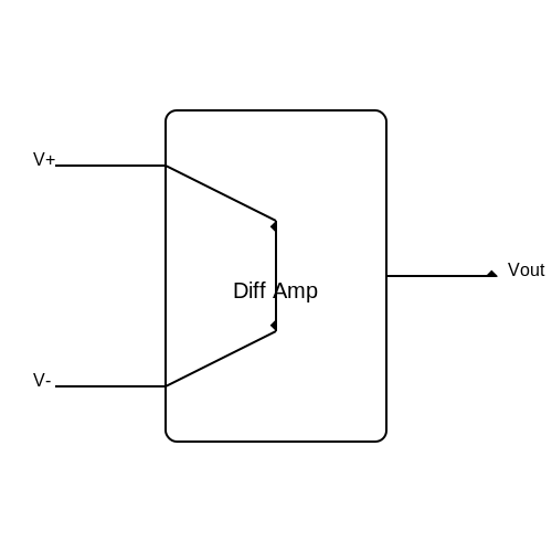
Differential amplification is the foundation of high-voltage differential probe operation, enabling precise measurement of voltage differences between two points while rejecting common-mode signals. The core principle relies on amplifying the difference between two input signals (V+ and V-) while attenuating any voltage common to both.
Mathematical Basis of Differential Amplification
The output voltage Vout of an ideal differential amplifier is given by:
where Ad is the differential gain and Ac is the common-mode gain. The quality of a differential amplifier is quantified by its common-mode rejection ratio (CMRR):
High-performance differential probes achieve CMRR values exceeding 80 dB at DC, decreasing with frequency due to parasitic capacitance imbalances.
Practical Implementation Challenges
Real-world differential amplifiers face several non-ideal characteristics that affect high-voltage measurements:
- Input impedance mismatch: Even small differences in input resistances (typically 1 MΩ ±1%) create common-mode conversion errors.
- Parasitic capacitance: Stray capacitances (1-5 pF typically) form frequency-dependent voltage dividers with the probe's input impedance.
- Nonlinearity: Semiconductor junctions in the input stage introduce distortion at high differential voltages.
The effective input impedance Zin of a differential probe is frequency-dependent:
where Rin is the input resistance (typically 1-10 MΩ) and Cin is the input capacitance (1-10 pF).
High-Voltage Design Considerations
For high-voltage applications (>1 kV), the amplifier topology must address:
- Voltage division: Precision resistor networks with matched temperature coefficients (α < 50 ppm/°C) maintain ratio stability.
- Isolation: Optocouplers or isolation amplifiers prevent ground loops while transmitting the differential signal.
- Breakdown protection: Gas discharge tubes or transient voltage suppressors (TVS) protect the front end from voltage spikes.
The maximum differential input voltage Vdiff,max is determined by:
where Pdiss is the power dissipation limit of the input stage and Ibias is the input bias current.
Frequency Response Limitations
The bandwidth of a differential probe is primarily constrained by:
where Rdiff and Cdiff are the differential path components, while Rcm and Ccm affect common-mode rejection. Modern high-voltage probes achieve bandwidths up to 200 MHz through careful layout optimization and compensation networks.
2.2 Isolation Techniques for High Voltage
Galvanic Isolation Principles
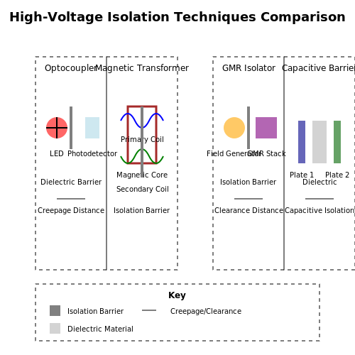
Galvanic isolation in high-voltage differential probes prevents unwanted current flow between the measurement circuit and ground, ensuring safety and signal integrity. The isolation barrier must withstand the full differential voltage while maintaining minimal capacitive coupling. The isolation voltage rating, typically ranging from 1 kV to 100 kV, is determined by the dielectric strength of the insulating material and the creepage/clearance distances.
where \( E_{\text{breakdown}} \) is the dielectric strength (V/m) and \( d \) is the insulation thickness. For example, a 1 mm air gap (breakdown strength ~3 kV/mm) provides ~3 kV isolation.
Optocoupler-Based Isolation
Optocouplers use an LED-photodetector pair to transmit signals across an optically transparent barrier. The LED converts the input signal to light, which the photodetector reconverts to an electrical signal. This method achieves isolation voltages up to 10 kV with bandwidths limited to ~10 MHz due to LED switching delays. Key parameters include:
- Current Transfer Ratio (CTR): Ratio of output to input current, typically 20-300%.
- Isolation Capacitance: ~1 pF, reducing high-frequency noise coupling.
Magnetic Isolation (Transformers & GMR)
Transformer-based isolation employs inductive coupling across a high-voltage barrier. Pulse transformers can achieve >100 kV isolation with bandwidths exceeding 100 MHz. Giant Magnetoresistance (GMR) isolators use magnetic field modulation for higher linearity, with typical specifications:
- Isolation Voltage: 5-15 kV
- Propagation Delay: <10 ns
- CMTI (Common-Mode Transient Immunity): >100 kV/µs
Capacitive Isolation
High-voltage capacitors (e.g., ceramic or polyimide) pass AC signals while blocking DC. A dual-capacitor topology cancels common-mode noise. The signal bandwidth is governed by:
where \( C_{\text{iso}} \) is typically 1-10 pF for minimal leakage. Silicon-dioxide-based capacitive isolators achieve 5 kV isolation with <0.5 pF coupling capacitance.
Dielectric Materials & Creepage Design
Critical for preventing arcing, creepage (surface distance) and clearance (air gap) follow IEC 61010 standards. For 1 kV RMS, minimum distances are:
- Creepage: 3.2 mm (pollution degree 2)
- Clearance: 1.5 mm
Common dielectrics include polyimide (300 V/µm), alumina (15 kV/mm), and silicone rubber (20 kV/mm). Multi-layer insulation with guard rings redistributes electric fields to avoid localized breakdown.
Practical Implementation Challenges
Real-world designs must account for:
- Partial Discharge: Micro-arcing in voids, mitigated by vacuum potting or SF6 filling.
- Thermal Runaway: Dielectric losses (\( P = V^2 \omega C \tan \delta \)) at high frequencies.
- EMI Coupling: Shielded enclosures and Faraday cages reduce radiated interference.
2.3 Common-Mode Rejection Ratio (CMRR) Explained
Definition and Mathematical Formulation
The Common-Mode Rejection Ratio (CMRR) quantifies a differential probe's ability to reject signals common to both inputs while amplifying the differential signal. It is defined as the ratio of the differential gain (Ad) to the common-mode gain (Acm):
In logarithmic terms (decibels), this becomes:
For an ideal differential probe, Acm approaches zero, making CMRR theoretically infinite. In practice, component mismatches and non-linearities limit CMRR.
Factors Affecting CMRR
The CMRR of a high-voltage differential probe is influenced by:
- Resistor matching: Mismatches in the input divider network degrade CMRR. A 1% mismatch can reduce CMRR to 40–60 dB.
- Amplifier imperfections: Op-amp input offset voltage and finite common-mode gain contribute to CMRR limitations.
- Parasitic capacitances: Uneven stray capacitances unbalance the probe's frequency response.
- Temperature drift: Thermal variations exacerbate resistor and amplifier mismatches.
Frequency Dependence of CMRR
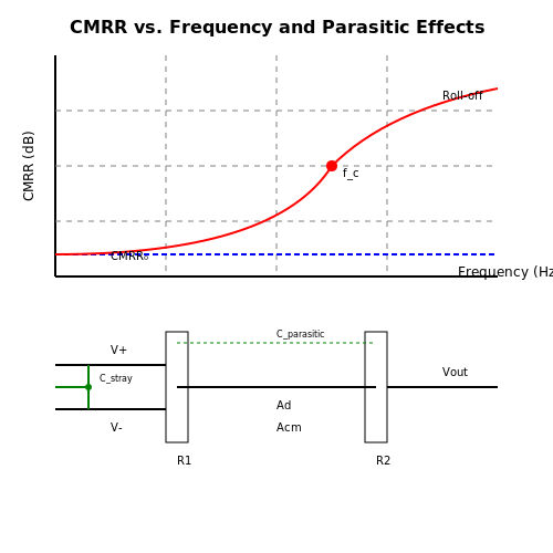
CMRR is not constant across frequencies. At higher frequencies, parasitic effects dominate, reducing rejection capability. The CMRR roll-off follows:
where fc is the corner frequency determined by the probe's bandwidth limitations. For example, a probe with fc = 1 MHz and CMRR0 = 80 dB at DC may exhibit only 60 dB rejection at 10 MHz.
Measurement Techniques
To empirically determine CMRR:
- Apply a common-mode signal (Vcm) to both inputs.
- Measure the output (Vout,cm).
- Apply a differential signal (Vd) and measure the output (Vout,d).
- Compute CMRR using:
Practical Implications
In high-voltage environments (e.g., power electronics testing), a low CMRR can lead to measurement errors when common-mode noise (e.g., switching transients) overwhelms the differential signal. For instance, a 1000 V common-mode spike with 60 dB CMRR appears as a 1 mV error at the output—significant when measuring millivolt-level differential signals.
Probes with >80 dB CMRR at DC and >60 dB at 1 MHz are preferred for precision measurements in noisy environments.
3. Power Electronics and Inverter Measurements
3.1 Power Electronics and Inverter Measurements
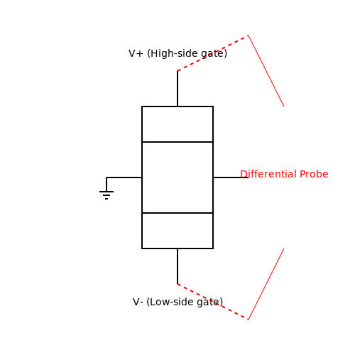
High-voltage differential probes are indispensable in power electronics for accurately measuring floating voltages in circuits such as inverters, motor drives, and switched-mode power supplies. Unlike single-ended probes, differential probes reject common-mode noise, enabling precise measurements in high-common-mode voltage environments.
Measurement Challenges in Power Electronics
Inverter topologies, such as three-phase voltage-source inverters (VSIs), generate high-frequency switching transients with common-mode voltages exceeding several kilovolts. A single-ended probe referenced to ground introduces measurement errors due to:
- Ground loop currents induced by high dV/dt switching.
- Common-mode rejection ratio (CMRR) degradation at high frequencies.
- Voltage divider imbalance caused by parasitic capacitances.
Differential Probe Operating Principles
The probe attenuates and isolates the input signal while maintaining high CMRR. The output voltage Vout is given by:
where G is the attenuation gain, V+ and V- are the differential inputs, and εCM is the common-mode error. For a probe with 1000:1 attenuation and 80 dB CMRR at 1 MHz, a 10 kV common-mode voltage appears as:
Critical Parameters for Inverter Measurements
- Bandwidth: Must exceed the switching frequency harmonics (e.g., ≥100 MHz for SiC/GaN inverters).
- Voltage range: Typical industrial probes support ±6 kV DC/peak AC.
- Input impedance: High impedance (≥10 MΩ) minimizes circuit loading.
Practical Measurement Example
When measuring a 3-phase inverter’s gate-source voltage (VGS), the probe’s bandwidth and rise time must resolve sub-100 ns transitions. For a 10 MHz signal with 50 ns rise time:
Calibration and Compensation
Probe accuracy depends on periodic calibration using a known differential voltage source. Compensation involves:
- Adjusting the probe’s DC offset nullification circuit.
- Matching input capacitances to maintain CMRR at high frequencies.
For high-precision measurements, temperature drift (typically ±0.1%/°C) must be accounted for in thermal environments.
3.2 Motor Drive and Switching Circuit Analysis
High-Voltage Switching Transients and Measurement Challenges
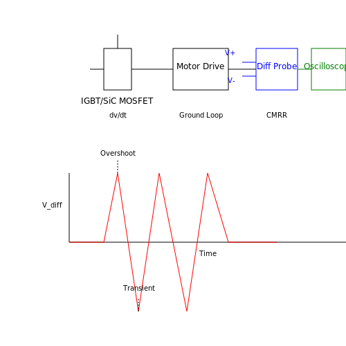
Switching circuits in motor drives generate fast high-voltage transients due to the rapid turn-on and turn-off of power semiconductors like IGBTs or SiC MOSFETs. These transients exhibit dv/dt rates exceeding 10 kV/µs, introducing significant common-mode noise and ground loop interference. Conventional single-ended probes fail to accurately capture these signals due to their limited common-mode rejection ratio (CMRR) and bandwidth constraints.
where V+ and V- are the potentials at the two measurement points. A high-voltage differential probe rejects common-mode signals by:
Probe Bandwidth and Rise Time Considerations
The probe's bandwidth must exceed the harmonic content of the switching waveform. For a pulse with rise time tr, the required bandwidth is:
For modern SiC-based inverters with tr = 20 ns, the probe requires at least 17.5 MHz bandwidth. However, to maintain signal fidelity, a 100 MHz or higher bandwidth is typically recommended.
Attenuation Ratio and Input Impedance
High-voltage probes use resistive dividers to scale down the input voltage. The attenuation ratio (R) must account for both the probe's internal impedance and the circuit under test:
where R1 is the high-impedance arm (typically 10 MΩ to 100 MΩ) and R2 is the low-impedance arm (1 kΩ to 10 kΩ). The probe's input capacitance (1–5 pF) must also be minimized to avoid distorting high-frequency signals.
Practical Measurement Techniques
When probing motor phase voltages:
- Minimize ground lead length to reduce inductive pick-up.
- Use matched probe pairs for multi-channel measurements to ensure phase alignment.
- Verify probe derating at high frequencies, as voltage ratings decrease with rising dv/dt.
Case Study: SiC Inverter Measurement
In a 1200 V SiC MOSFET bridge, the drain-source voltage exhibits overshoot due to parasitic inductance. A 1000:1 differential probe with 200 MHz bandwidth captures this transient, revealing a 150 V overshoot lasting 50 ns. The measurement setup requires:
- Differential connection across the switch
- Isolated power supply for the probe
- Oscilloscope with 1 MΩ input impedance
Thermal and Safety Considerations
High-voltage probes must withstand the thermal environment of motor drives, where ambient temperatures can exceed 85°C. The probe's insulation rating (e.g., CAT III 1000 V) must match the system's voltage class. Additionally, creepage and clearance distances must comply with IEC 61010-1 to prevent arcing.
3.3 High-Frequency Signal Integrity Testing
High-voltage differential probes must maintain signal integrity when measuring high-frequency waveforms, particularly in applications such as power electronics, RF systems, and high-speed digital circuits. At frequencies exceeding 100 MHz, parasitic capacitances, transmission line effects, and probe loading become critical factors.
Bandwidth and Rise Time Considerations
The bandwidth (BW) of a differential probe is determined by its internal resistance (R) and capacitance (C), forming a first-order low-pass filter response:
For accurate measurements, the probe's rise time (tr) must be significantly faster than the signal's rise time. The relationship between bandwidth and rise time is approximated by:
A probe with a 1 GHz bandwidth, for instance, has a theoretical rise time of 350 ps. If the measured signal has a rise time below 1 ns, this probe would introduce minimal distortion.
Transmission Line Effects and Impedance Matching
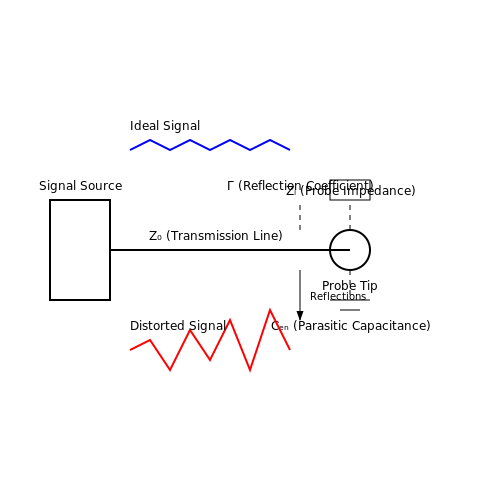
At high frequencies, the probe's input impedance must match the characteristic impedance (Z0) of the transmission line to prevent reflections. Mismatched impedance leads to standing waves, distorting the measured waveform. The reflection coefficient (Γ) is given by:
where ZL is the probe's input impedance. For minimal reflections, ZL should closely match Z0 (typically 50 Ω or 1 MΩ in parallel with a few pF).
Parasitic Capacitance and Loading Effects
Probe capacitance (Cin) forms a parallel RC network with the circuit under test, attenuating high-frequency components. The capacitive reactance (XC) is:
For a 1 pF probe at 1 GHz, XC ≈ 159 Ω, significantly loading low-impedance circuits. Active differential probes mitigate this with FET-based buffers, reducing Cin to sub-picofarad levels.
Common-Mode Rejection Ratio (CMRR) at High Frequencies
CMRR degrades with frequency due to parasitic imbalances in the probe's internal circuitry. The frequency-dependent CMRR is modeled as:
where α is a parasitic asymmetry factor. High-performance probes maintain >60 dB CMRR up to 1 GHz, critical for measuring small differential signals in noisy environments.
Practical Measurement Techniques
To minimize high-frequency artifacts:
- Use the shortest possible ground leads to reduce inductance.
- Verify probe compensation before measurements using a calibration square wave.
- Select probes with bandwidth ≥5× the signal's highest harmonic to capture fast edges accurately.
4. Safety Precautions for High-Voltage Measurements
4.1 Safety Precautions for High-Voltage Measurements
Working with high-voltage differential probes requires stringent safety protocols due to the inherent risks of electric shock, arc flash, and equipment damage. Voltages exceeding 30V RMS or 42.4V peak are considered hazardous under IEC 61010 standards, necessitating proper insulation, grounding, and personal protective equipment (PPE).
Insulation and Clearance Requirements
The minimum creepage and clearance distances scale nonlinearly with voltage. For a 1kV measurement in pollution degree 2 (normal indoor conditions), IEC 60664-1 specifies:
Where Vpeak includes any transient overvoltages. For reinforced insulation at 1kV, this yields 8.3mm clearance and 10.4mm creepage minimums. Practical designs should exceed these values by 20-50%.
Grounding and Isolation
Differential probes must maintain:
- Galvanic isolation ≥ 2x the measured voltage between probe channels
- Guard rings around high-impedance inputs to prevent surface leakage
- Single-point grounding of the measurement system to avoid ground loops
The isolation impedance Ziso should satisfy:
Where Ileakage is typically limited to 100μA for personnel safety.
Personal Protective Equipment
When measuring voltages above 300V:
- Wear Class 00 rubber gloves (tested to 2.5kV) with leather protectors
- Use ANSI Z87.1 rated face shields when arc flash risk exists
- Employ FR-rated clothing for measurements exceeding 600V
Probe Handling Procedures
Proper technique minimizes risks:
- Always connect the ground lead first and remove it last
- Keep one hand in a pocket to prevent current paths through the chest
- Verify probe derating curves - most 1kV probes are rated for ≤300V at 100MHz
The transient response time tr affects safe measurement bandwidth:
Where exceeding Vrated by 2x typically reduces bandwidth by 40%.
4.2 Calibration and Maintenance Procedures
Calibration Methodology
High-voltage differential probes require periodic calibration to ensure measurement accuracy, particularly due to component aging and thermal drift. The calibration process involves verifying both the attenuation ratio and common-mode rejection ratio (CMRR) across the probe's operational bandwidth.
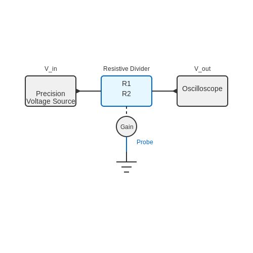
Where \( R_1 \) and \( R_2 \) form the resistive divider network. Calibration is performed using a precision voltage source, with known input voltages (\( V_{\text{in}} \)) compared against the probe's output (\( V_{\text{out}} \)) on an oscilloscope. A deviation beyond ±1% typically necessitates adjustment.
Step-by-Step Calibration
- Warm-up: Power on the probe and allow it to stabilize for at least 15 minutes to minimize thermal drift effects.
- Zero Adjustment: Ground both inputs and adjust the offset potentiometer until the output reads 0V ± 1mV.
- Gain Calibration: Apply a known DC voltage (e.g., 100V) and adjust the gain potentiometer until the output matches the expected attenuation ratio.
- Frequency Response Verification: Use a function generator to sweep frequencies from 10Hz to the probe's rated bandwidth, ensuring consistent attenuation.
CMRR Calibration
Common-mode rejection is critical for noise immunity. To calibrate:
where \( V_{\text{cm}} \) is the applied common-mode voltage, and \( V_{\text{err}} \) is the erroneous differential output. A CMRR below 60dB at 1MHz indicates degradation.
Maintenance Procedures
- Cleaning: Use isopropyl alcohol on input connectors to prevent oxidation-induced contact resistance.
- Storage: Keep probes in a low-humidity environment to prevent dielectric absorption in high-voltage dividers.
- Periodic Verification: Perform a quick gain/offset check monthly if used in critical applications.
Case Study: Thermal Drift Compensation
In a 2021 study by IEEE Transactions on Instrumentation, active thermal compensation circuits reduced drift in high-voltage probes by 78%. The method involved embedding a temperature sensor near the divider network and dynamically adjusting gain via a microcontroller.
Troubleshooting Common Issues
| Issue | Diagnosis | Solution |
|---|---|---|
| Nonlinear output | Degraded resistor network | Replace divider assembly |
| High-frequency roll-off | Parasitic capacitance | Recalibrate compensation capacitors |
For probes with active components (e.g., FET-input amplifiers), check power supply ripple and replace aging electrolytic capacitors every 5 years.
4.3 Grounding and Noise Reduction Techniques
Proper grounding is critical when using high-voltage differential probes to minimize common-mode noise and ensure accurate measurements. A floating ground reference or improper grounding can introduce significant measurement errors, particularly in high-frequency or high-impedance circuits.
Ground Loop Mitigation
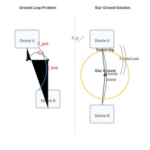
Ground loops occur when multiple ground paths create circulating currents, inducing unwanted noise. For differential probes, the ground connection should be a single-point reference. The voltage drop Vgnd across a ground impedance Zg due to a current Iloop is given by:
To minimize this effect:
- Use a star-ground configuration where all ground connections meet at a single point.
- Avoid long ground leads, which increase inductance and susceptibility to electromagnetic interference (EMI).
- Employ isolation transformers or optocouplers in systems where ground potential differences exceed the probe's common-mode range.
Common-Mode Rejection Ratio (CMRR)
The effectiveness of a differential probe in rejecting common-mode signals is quantified by its CMRR, defined as:
where Ad is the differential gain and Acm is the common-mode gain. High CMRR (>80 dB at DC) is essential for accurate high-voltage measurements. However, CMRR degrades with frequency due to parasitic capacitances:
where τ is the time constant of the probe's input stage.
Shielding and Guarding
Electrostatic shielding reduces capacitive coupling from external noise sources. A guard ring, held at the same potential as the high-impedance input, minimizes leakage currents. The leakage current Ileak through a parasitic capacitance Cp is:
Guarding effectively reduces Cp by surrounding the sensitive node with a conductor at the same potential.
Twisted-Pair and Coaxial Cabling
For long signal paths, twisted-pair wiring reduces magnetic interference by ensuring loop areas between conductors are minimized. The induced noise voltage Vnoise from a magnetic field B is:
where A is the loop area. Coaxial cables provide superior shielding above 1 MHz, with their transfer impedance ZT dictating shielding effectiveness:
Active Guard Drive
Advanced probes use active guard drives to bootstrap the shield potential, reducing capacitive loading. The guard amplifier ensures the shield follows the input signal, minimizing the voltage across Cp. This technique is particularly effective in high-impedance (>1 MΩ) applications.
Noise Filtering Techniques
Post-measurement digital filtering (e.g., moving average, FIR) can further reduce noise, but analog filtering at the probe input is preferable to avoid aliasing. A first-order RC filter's cutoff frequency is:
For high-voltage applications, ensure filter components are rated for the full voltage range.
5. Recommended Books and Technical Papers
5.1 Recommended Books and Technical Papers
- PDF P6250 & P6251 500 MHz and 1 GHz High Voltage Differential Probes ... — This is the Technical Reference for the P6250 & P6251 differential probes. This manual provides specifications and performance verification procedures for the probes.
- PDF TDP0500 & TDP1000 High Voltage Differential Probes Technical Reference — This is the Technical Reference Manual for the TDP0500 & TDP1000 differential probes. This manual provides specifications and performance verification procedures for the probes.
- PDF TDP1500 1.5 GHz Differential Probe Technical Reference — The specifications in Tables 1 through 4 apply to a TDP1500 differential probe installed on a Tektronix DPO7000 oscilloscope. When the probe is used with another oscilloscope, the oscilloscope must have an input impedance of 50 Ω and a bandwidth of 1 GHz.
- PDF High Voltage Engineering - Helsinki — As in the previous edition, the principal objective of the current text is to cover the fundamentals of high-voltage laboratory techniques, to provide an understanding of high-voltage phenomena, and to present the basics of high-voltage insulation design together with the analytical and modern numerical tools available to high-voltage equipment designers.
- PDF AR372 Choosing the right differential probe - Pico Tech — Pico Technology offers many active differential probes covering a wide range of voltages, category (CAT) ratings and bandwidths. As the name suggests, these probes have two major features: Active: Active probes achieve low input capacitance and high sensitivity by buffering and amplifying the signal close to the point of measurement.
- PDF P5200A Series High Voltage Differential Probes Instruction Manual — This section explains the operating characteristics of the P5200A Series High Voltage Differential Probes and includes techniques that you can use to maximize the performance of the probe.
- PDF HIGH VOLTAGE - download.e-bookshelf.de — The contents of this book are derived from the lectures in High Voltage Engineering delivered by us for decades at Technical University (TU) Dresden, Germany and at Indian Institute of Technology, Kanpur, India, to the graduate and senior undergraduate students. Our fi rst book in English on the subject was published in 1995 in India. Since then, much research and development work have been ...
- PDF HVD3000 Series High Voltage Differential Probe Operator's Manual — The HVD3000 and HVD3000A high-voltage active differential probes are safe, easy-to-use, and ideally suited for power electronics applications where the reference potential is elevated from ground.
- PDF General TI High Voltage Evaluation User Safety Guidelines — General TI High Voltage Evaluation User Safety Guidelines WARNING Always follow TI's set-up and application instructions, including use of all interface components within their recommended electrical rated voltage and power limits.
- PDF High-Voltage Test and Measuring Techniques — Foreword to the First Edition Most textbooks on high-voltage (HV) engineering published in the recent years are focused on general aspects of this eld but not on the specics of HV test and fi fi measuring techniques provided in this book.
5.2 Industry Standards and Compliance Documents
- PDF IS/IEC 60060-2 (2010): High - Voltage Test Techniques, Part 2 ... — Indian Standard HIGH-VOLTAGE TEST TECHNIQUES PART 2 MEASURING SYSTEMS ICS 17.220.20;19.080 IS/IEC 60060-2 : 2010 ... The following referenced documents are indispensable for the application of this standard. For ... NOTE An electric-field probe may be used to measure the waveform of the voltage producing the field provided
- PDF Keysight Technologies N2804A and N2805A High Voltage Differential Probes — The N2804A 300-MHz differential probe offers 100:1 attenuation ratio, allowing it to be used adequately for high voltage signal measurements. The differential probe has a differential input resistance of 4 MΩ and low input capacitance of 4 pF to minimize circuit loading. The probe
- PDF Requirements for Soldered Electrical and Electronic Assemblies — Electronic Assemblies Developedby the J-STD-001Task Group(5-22a)of the Soldering Subcommittee(5-22) of the Assembly& JoiningCommittee(5-20) of IPC Usersof this publicationare encouragedto participatein the developmentof futurerevisions. Contact: IPC Supersedes: J-STD-001F WAM1 - February 2016 J-STD-001F - July 2014 J-STD-001E - April 2010
- PDF Frequently Asked Questions - North American Electric Reliability ... — Compliance will continue to be determined based on ... including dated electronic or physical lists of the high and medium impact BES Cyber Systems." 52 . CIP-002-5.1 ; Requirement R1 . Attachment 1 . ... operating voltage of the tie line the meter is reporting. 77 ; CIP V5 FAQs - Consolidated FAQs and Answers - October 2015 3 ...
- PDF AN-1031 TIA/EIA-422-B Overview (Rev. B) - Texas Instruments — rates (see Figure 3 ). Standard RS-422drivers are assured to source and sink a minimum 20 mA across a 100 Ωload. This corresponds to a minimum differential output voltage, VOD, of 2 V across the load (see Figure 1). Figure 1. Terminated Configuration The complement RS-422receiver must be equal to or less than one unit load. This is represented ...
- High-Voltage Differential Probe - Circuit Cellar — Amplifiers in Action A high-voltage differential probe is a critical piece of test equipment for looking at high-voltage signals. In his article, Andrew describes his design of a high-voltage differential probe with features similar to commercial devices, but at a considerably lower cost. It uses just three op amps in a classic instrumentation amplifier configuration […]
- PDF N2790A Differential Voltage Probe User's Guide - Keysight — A Probe Tip Accessory Kit (consisting of 2 browser tips, 2 pincher clips, and 2 alligator plunger tips), can be ordered as part number N2790-68700. Replacement probe tips are not orderable separately. The supplied accessories are for use only with the N2790A differential voltage probe. Figure 1 Probe with Supplied Accessories
- PDF N2804/5A Differential Probes User's Guide - Keysight — The N2804A 300 MHz differential probe offers 100:1 attenuation ratio, allowing it to be used for high voltage signal measurements. The differential probe has an differential input resistance of 4 M W and low input capacitance of 4 pF to minimize circuit loading. The probe comes with a pair of extension leads (30 cm long) with a
- PDF AR372 Choosing the right differential probe - Pico Tech — measurements focus exclusively on the potential difference between the probes. A differential probe must always be operated within its voltage limits. These are explained under Input ranges below. 3. Using the probe for single-ended measurements An often overlooked fact is that the active differential probe excels at making single-ended ...
- PDF LVDS Owner's Manual - Texas Instruments — ational Semiconductor's LVDS Owner's Manual, first published in spring 1997, has been the industry's "go-to design guide" over the last decade. The owner's manual helped LVDS grow from the original IEEE 1596.3-1996 Standard for Low-Voltage Differential Signaling (LVDS) for Scalable Coherent Interface (SCI) into the workhorse
5.3 Online Resources and Tutorials
- Tips and tricks for high-speed, high-voltage measurement — amplifier and still maintain the capability for high-voltage measurement, adding a wideband, low-capacitance voltage attenuator is also required. The VCA824 from Texas Instruments is an example of a wideband, fully-differential amplifier with high input impedance that can drive 50-W lines. It has an input common-mode range of ±1.5 V and a
- Wide Bandgap Monthly Insights - March 2025 - Power Electronics News — Keysight's isolated differential probes offer up to 10 billion times superior common-mode rejection compared to traditional differential probes, rendering them optimal for high-voltage, high-side measurements. These probes provide precise investigation of fast-switching GaN and SiC devices, with a bandwidth of up to 1 GHz and a differential ...
- PDF AR372 Choosing the right differential probe - Pico Tech — Active differential probes often have switch-selectable attenuation, with the higher voltage probes having up to 1:100 and 1:1000 times attenuation. Each attenuation setting has its own differential-mode range. The Pico Technology range of active differential probes starts from ±15 V DC+AC peak with no switchable attenuation, to
- A High-Voltage and Low-Noise Power Amplifier for Driving ... - MDPI — In this paper, based on the principles of general operational amplifiers, a high-voltage operational amplifier is developed. Considering the influences of piezoelectric stack actuators on the circuit, a novel structure using the high-voltage operational amplifier as a noninverting amplifier is proposed. Because of the simple circuit principles and the voltage feedback control structure, the ...
- 5.4: Voltage Divider Bias - Engineering LibreTexts — 5.4.2: PNP Voltage Divider Bias. Method One; Method Two; Another configuration that can provide high bias stability is voltage divider bias. Instead of using a negative supply off of the emitter resistor, like two-supply emitter bias, this configuration returns the emitter resistor to ground and raises the base voltage.
- Digital electronics - Wikipedia — Digital electronics is a field of electronics involving the study of digital signals and the engineering of devices that use or produce them. It deals with the relationship between binary inputs and outputs by passing electrical signals through logical gates, resistors, capacitors, amplifiers, and other electrical components.The field of digital electronics is in contrast to analog electronics ...
- PDF Analogue Design And Simulation Using Orcad Capture And Pspice Copy — DC sweep or transient analysis would be suitable. A DC sweep varies the input voltage and shows the output response, while a transient analysis shows the circuit's response over time to a specific input waveform. Define Simulation Parameters: Set the relevant parameters for your chosen analysis. For a DC sweep, define the voltage range.
- Circumferential Crack Detection in Ultra-High-Pressure Tubular ... - MDPI — Ultra-high-pressure tubular reactors are crucial pieces of equipment for polyethylene production. Long-term operation under high temperature, high pressure, and other extremely harsh conditions can lead to various defects, with circumferential cracks posing a major safety risk. Detecting cracks is challenging, particularly when they are under a protective layer of a certain thickness. This ...
- A practical introduction to radio frequency electronics for NMR probe ... — The design of NMR probes is a specialized application of radiofrequency (rf) electronics. Many of the classic references on this topic are rich in information, but were intended for different audiences, e.g., post WWII radio engineers [1].The purpose of this tutorial paper is to present an introduction to some general principles that are pertinent to probe design.