Applied OrCAD
1. What is OrCAD?
1.1 What is OrCAD?
OrCAD is a powerful and widely used suite of software tools designed for electronic design automation (EDA). Developed by Cadence Design Systems, OrCAD provides engineers and researchers with the means to create, simulate, and analyze electronic schematics and printed circuit board (PCB) layouts efficiently. The software encompasses a range of functionalities that streamline the design process, ultimately contributing to more effective and reliable electronic products.
Initially released in the early 1980s, OrCAD has significantly evolved, acquiring robust simulation capabilities, integrated libraries, and a user-friendly interface. This extensive evolution has made it a staple in both academic and industrial environments for circuit design.
Key Features of OrCAD
The OrCAD suite incorporates several key applications, each serving distinct purposes in the electronic design process:
- OrCAD Capture: This part of the suite facilitates schematic capture, allowing designers to create circuit diagrams using a library of pre-defined components. The intuitive drag-and-drop functionality makes it accessible for users of varying expertise.
- OrCAD PCB Designer: This advanced tool focuses on creating PCB layouts from the schematics generated in OrCAD Capture. It includes features like auto-router and design rule check (DRC) to ensure manufacturability and functionality.
- OrCAD PSpice: PSpice provides powerful simulation capabilities, enabling users to predict the behavior of their designs under various conditions. This is crucial for validating design choices before fabrication.
- OrCAD Manufacturing Output: This feature produces necessary files such as Gerber files and Bill of Materials (BOM) required for PCB fabrication and assembly.
Real-World Applications
The practical relevance of OrCAD extends across numerous industries, including consumer electronics, automotive, telecommunications, and medical devices. Engineers use OrCAD to design everything from simple circuit boards for hobby projects to complex systems for cutting-edge technologies such as electric vehicles and advanced communication systems.
In educational settings, OrCAD serves as an invaluable tool for teaching circuit design concepts and practical applications. Students familiar with OrCAD develop skills that are directly applicable in the workforce, enhancing their employability in an increasingly technology-driven world.
Transition to Advanced Applications
As complex electronic systems become the norm, the need for precision in design and verification has never been greater. In this context, OrCAD’s integration with other Cadence tools, such as Allegro for PCB design and Sigrity for power integrity analysis, reflects the essential role of comprehensive design solutions in managing intricate projects.
In the following sections, we will explore specific functionalities of OrCAD, delve into practical usage scenarios, and analyze the implications of simulation techniques to enhance electronic design workflows.
1.2 Applications of OrCAD in Electronics
Introduction to OrCAD in Electronic Design
OrCAD is a powerful suite of software tools utilized in electronic design automation (EDA), primarily for the creation of schematics and printed circuit boards (PCBs). Its advanced features allow engineers to streamline the design process, enabling the efficient transition from concept to prototype.
1. Circuit Simulation and Analysis
One of the most significant applications of OrCAD is in circuit simulation, utilizing tools like OrCAD PSpice. This allows engineers to validate their designs under various conditions before physical prototyping. The PSpice simulator operates on the principle of analyzing electrical circuits using methods such as nodal analysis and transient analysis. This simulation capability is crucial for observing circuit behavior, verifying performance metrics, and identifying potential issues, significantly reducing development costs and time-to-market.
Validation Through Simulation
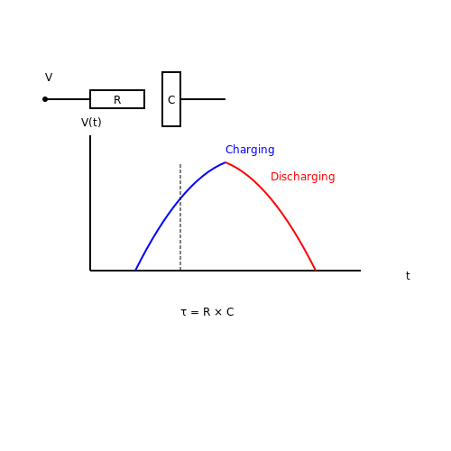
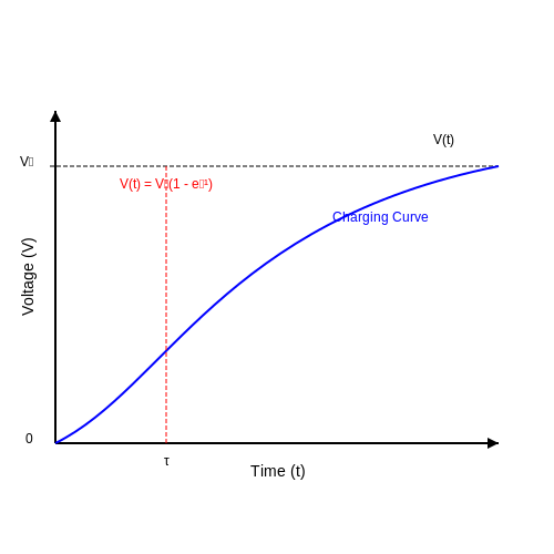
For instance, consider a simple RC (resistor-capacitor) circuit. By leveraging OrCAD PSpice, engineers can simulate the time constant and observe output waveform behaviors. This ensures that the real-world performance aligns with theoretical expectations.
Where:
- τ is the time constant (in seconds)
- R is the resistance (in ohms)
- C is the capacitance (in farads)
2. PCB Layout and Design
OrCAD is also widely recognized for its PCB design capabilities, which encompass layout, routing, and verification. The OrCAD PCB Designer allows users to create complex multi-layer designs with real-time design rule checks (DRC), ensuring compliance with manufacturing standards. The layer stack-up features facilitate the design of high-speed circuits while minimizing parasitic effects, such as inductance and capacitance, that could adversely affect performance.
Design Rule Checks (DRC)
Design rule checks are integral in the PCB design process to avoid costly manufacturing errors. OrCAD ensures that width and spacing adhere to the specifications needed for different layer types, grounding requirements, and signal integrity constraints.
3. Integration of Manufacturing Data
Another vital application of OrCAD is its capacity to generate comprehensive fabrication and assembly outputs. By using OrCAD's integrated tools, designers can produce Gerber files, drill files, and BOMs (bills of materials) essential for the manufacturing processes. This ensures seamless communication between the design team and manufacturers, thereby facilitating accurate and efficient production.
Case Study: Collaborative Electronic Product Development
Consider a collaboration scenario where multiple teams work on a consumer electronics product. Utilizing OrCAD, teams can share and iterate on design files seamlessly, enabling quick adjustments based on both functional requirements and manufacturing constraints, leading to faster product iterations and improved final products.
4. Advanced Simulation Features
The software offers extensive simulation capabilities beyond basic circuit analysis. Features like Monte Carlo analysis and temperature variability simulations allow engineers to understand how component tolerances can affect circuit performance under different environmental conditions. This approach aligns with practices in reliability engineering, where understanding the limits and behaviors of components is crucial for product longevity and customer satisfaction.
Conclusion
In summary, OrCAD plays a pivotal role in various domains of electronics, from initial concept validation through simulation to final manufacturing output. Its robust toolset empowers engineers to optimize designs efficiently, adhere to industry standards, and bring innovative products to market with reduced risk and enhanced reliability.
1.3 Tools and Features Overview
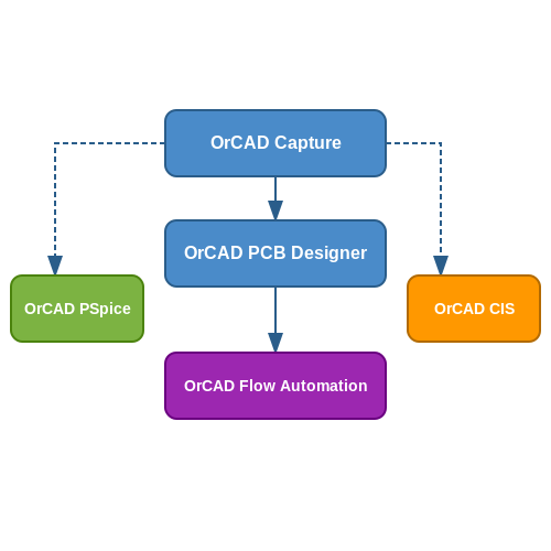
In this section, we delve into the sophisticated ecosystem of OrCAD, a vital tool for contemporary electrical and electronic engineering design. OrCAD encompasses a suite of powerful tools that streamline the design process from schematic creation to PCB layout and beyond. Understanding each tool and its features enables engineers, physicists, and researchers to maximize their productivity and design efficiency.Design Tools
OrCAD provides a rich selection of design tools that cater to various stages of the design process:- OrCAD Capture: This intuitive schematic capture tool allows engineers to create and edit electronic schematics. It supports hierarchical design methodologies, enabling complex designs to be divided into manageable subcircuits. The built-in libraries provide access to a vast array of components, ensuring that designers have everything they need at their fingertips.
- OrCAD PCB Designer: Following schematic creation, PCB Designer facilitates the conversion of schematics into printed circuit board layouts. This tool offers advanced routing capabilities, including autorouting, differential pair routing, and a powerful DRC engine to ensure that all design rules are adhered to.
- OrCAD PSpice: This simulation tool is pivotal for validating designs before fabrication. Engineers can predict circuit behavior through simulation, using both DC and AC analyses, transient simulation, and even advanced features for mixed-signal designs. PSpice includes modeling capabilities for a variety of components, allowing for accurate representation of real-world behavior.
Analysis Features
By employing OrCAD, engineers gain access to comprehensive analysis features that are essential for optimizing circuit performance.- Sensitivity Analysis: This feature allows users to evaluate how changes in component values affect circuit performance. By systematically varying parameters, designers can identify sensitive points within their circuits, enabling targeted improvements.
- Monte Carlo Analyses: OrCAD supports Monte Carlo simulations, which are invaluable for assessing the performance variability of a design under statistical variations in component values. Such insights are essential in fields like automotive and aerospace, where reliability is paramount.
- DC and AC Sweep Analysis: This facilitates the examination of circuit behavior over a range of input values. For instance, engineers can characterize the frequency response of amplifiers or other AC-coupled circuits, providing insight into threshold levels and gain performance.
Collaboration and Integration
Modern engineering often demands collaboration across disciplines. OrCAD integrates seamlessly with various data management systems and offers tools for version control and team collaboration.- OrCAD CIS: This tool enhances design productivity by providing the capability to manage component information effectively. It links schematics with parts management systems, ensuring that component selections are optimized and up-to-date.
- OrCAD Flow Automation: Design processes can be automated through OrCAD’s scripting capabilities. By creating scripts, repetitive tasks can be streamlined, reducing errors and saving time, which is critical in fast-paced project environments.
- Integration with CAD tools: OrCAD can integrate with various CAD applications, enabling engineers to import/export designs between platforms, thus facilitating cross-disciplinary workflow efficiencies. This interoperability is crucial for larger projects that involve multiple engineering teams.
2. System Requirements
2.1 System Requirements
In the realm of electronic design automation (EDA), OrCAD stands as a pivotal tool in circuit design, providing integrated environments for simulation, schematic capture, and PCB design. However, maximizing the potential of OrCAD necessitates a clear understanding of the system requirements that ensure optimal performance. Starting with the operating environment, OrCAD runs primarily on Windows platforms. As of the latest releases up to October 2023, the minimum requirement dictates a 64-bit version of Windows 10 or later. This is critical as 64-bit systems can handle larger memory allocations, which are immensely beneficial during complex simulations. It is also recommended to stay updated with the latest service packs and patches from Microsoft. Next, let us delve into the processor specifications. A multi-core processor is advisable; typically, a dual-core processor serves as the minimum, but for rigorous tasks such as PCB design and simulation, a quad-core or higher processor is preferable. The benefits are evident: simulations can run significantly faster, and multitasking becomes more manageable. When discussing memory, OrCAD applications can be quite demanding. A minimum of 8 GB of RAM is essential for basic operations; however, for professionals working on advanced projects, 16 GB or more is suggested. This ensures that multiple applications can run concurrently without significant slowdowns, especially when handling large design files. Storage requirements are another critical aspect. A solid-state drive (SSD) is highly recommended over traditional hard drives (HDD) as it offers superior read and write speeds, which translates to faster loading times for projects and software. Typically, at least 100 GB of free space is necessary, although having more is beneficial to accommodate project files and simulations. In terms of graphical requirements, an advanced graphics card is an important consideration. While integrated graphics can handle basic tasks, a dedicated GPU ensures that OrCAD can render 3D models smoothly and provide a better visual representation of circuit designs. OpenGL support is a must; hence, choosing a graphics card from reputable manufacturers such as NVIDIA or AMD is recommended. Finally, network connectivity should not be overlooked, particularly for collaborative projects. A stable internet connection is essential, especially if utilizing cloud features or remote server access for simulations and storage. The essence of these requirements culminates in a reliable and efficient working environment, allowing engineers and designers to focus on their core tasks without the frustration of hardware lag or compatibility issues. By adhering to these specifications, a user can leverage OrCAD to its fullest potential, resulting in high-performance outputs that meet the demanding standards of the electronics industry. Overall, a harmonious balance of processor power, ample memory, efficient storage solutions, and a capable graphics system will foster an effective and productive design environment with OrCAD.2.2 Installation Process
The installation of OrCAD is a structured process, designed to cater to various system configurations and user needs. As an advanced-level reader, you will find this tutorial provides detailed steps, essential for a successful setup, along with tips on optimizing the environment for your specific projects.
System Requirements
Before diving into the installation, it is crucial to ascertain that your system meets the necessary requirements. OrCAD is resource-intensive, and overlooking the system specifications might lead to subpar performance. The following are standard requirements:
- Operating System: Windows 10 or later, or suitable compatibility layers for other OS.
- Processor: Minimum quad-core processor.
- RAM: At least 8 GB, with 16 GB recommended.
- Disk Space: Approximately 10 GB of free space for installation and temporary files.
Confirming these specifications ensures that you avoid common pitfalls that can arise from insufficient resources.
Installation Steps
The installation process can be broken down into several clear stages that ensure efficiency and minimize errors:
- Download OrCAD: Begin by acquiring the official OrCAD installer from the OrCAD official website. Ensure you select the version appropriate for your needs, keeping in mind the licensing options available.
- Run the Installer: Navigate to your downloads folder and double-click the installer. If prompted by User Account Control (UAC), click 'Yes' to allow changes.
- License Agreement: Carefully read the terms of use presented in the installation wizard. Agree to the terms to proceed.
- Select Components: You will be prompted to choose which components of OrCAD to install. This typically includes OrCAD Capture, PCB Editor, and other modules based on your requirement.
- Installation Path: Choose an installation path or proceed with the default. Custom paths can help organize projects more intuitively.
- Install: Begin the installation. This might take several minutes depending on the speed of your system. Do not interrupt the process to avoid corrupting the installation files.
- Finalization: Once the installation is complete, reboot your computer if required. Upon logging in, you should find OrCAD in your application list.
Post-Installation Configuration
After installation, it is vital to configure OrCAD for optimal performance:
- Workspace Setup: Familiarize yourself with the user interface and set up your workspace to enhance productivity.
- Library Management: Import necessary libraries and ensure that your projects have access to required components.
- Activate License: Launch the application to input your license key, enabling full functionality.
These configurations are essential as they set the groundwork for your design environment, allowing you to leverage the full power of OrCAD for complex engineering projects.
By following these installation steps meticulously, you will ensure that your OrCAD environment is ready for advanced work, equipped with the tools necessary for tackling sophisticated design challenges.
2.3 Configuration Settings
In the realm of electronic design automation, configuration settings in OrCAD play a pivotal role in customizing the tool's functionality according to specific design requirements. By effectively configuring these settings, designers can streamline their workflow, address specific project needs, and enhance simulation accuracy.
When first entering the configuration section of OrCAD, users are presented with a plethora of options that can be tailored. These settings encompass various aspects, including global preferences, user interface preferences, and simulation parameters. Each of these settings influences how projects are managed and interacted with in OrCAD.
Global Preferences
The global preferences setting governs the overall behavior of OrCAD tools. Key areas include:
- File Management: Here, users can specify default directories for design files, libraries, and projects. Utilizing organized file structures not only enhances accessibility but also minimizes errors due to missing files.
- Update Options: This portion controls how OrCAD checks for updates, allowing users to maintain the latest features and bug fixes. Keeping software updated is critical in maintaining compatibility with industry standards.
- Color Themes: A customizable workspace can significantly improve the user experience and reduce visual fatigue during long design sessions.
Simulation Settings
Another crucial configuration area is simulation settings, which directly influence the accuracy and efficiency of simulations:
- Solver Selection: OrCAD allows users to select different solvers based on the type of analysis being performed, such as linear or nonlinear analysis, thereby optimizing simulation performance.
- Convergence Parameters: Fine-tuning convergence settings can help resolve issues when simulating complex circuits with non-ideal components. This is particularly important in designs with mixed-signal components.
- Component Models: Users can choose specific model libraries which are better suited for the unique characteristics of components employed in their designs. Utilizing accurate models ensures that simulation results reflect real-world behavior.
User Interface Preferences
OrCAD's user interface can also be customized to fit the workflow of individual designers:
- Toolbars and Menus: Designers can streamline their workflows by showing or hiding specific toolbars and menus, giving priority to the tools they use most frequently.
- Shortcut Keys: Customizing keyboard shortcuts can lead to a more efficient workflow by reducing the time spent navigating through menus.
The impact of these configuration settings extends to real-world applications. For instance, within industries such as aerospace or automotive, precise simulation outcomes derived from correctly configured settings can lead to significant improvements in product reliability and performance while decreasing time-to-market.
By thoroughly understanding and utilizing the configuration settings in OrCAD, advanced users can enhance their efficiency and the integrity of their designs, ultimately contributing to the success of their projects.
3. Creating New Schematics
3.1 Creating New Schematics
In the realm of electronics design, creating new schematics serves as a fundamental skill that lays the groundwork for circuit development and simulation. With OrCAD, users benefit from an array of features designed to streamline schematic design while enabling complex circuit modeling. By understanding the nuances of OrCAD, engineers can efficiently translate their theoretical designs into practical schematics, which can later be utilized for PCB layout and simulations.
Understanding the OrCAD Environment
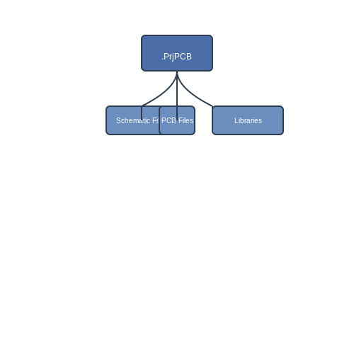
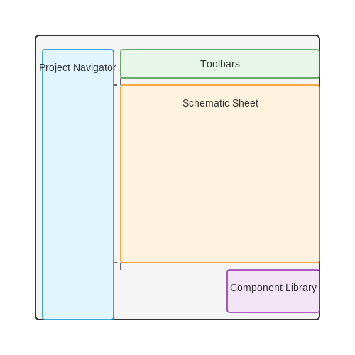
Before embarking on schematic creation, it is essential to familiarize oneself with the OrCAD interface. Upon launching OrCAD Capture, the user is greeted with a workspace consisting of various toolbars, panels, and menus that provide quick access to drawing tools, libraries, and design functionalities. The Project Navigator is particularly important as it allows users to organize their designs, access schematic sheets, and manage libraries.
Starting a New Schematic
To create a new schematic in OrCAD Capture, follow these steps:
- Launch OrCAD Capture and select File → New → Project.
- In the dialog that appears, choose Schematic as the project type and provide a relevant name.
- After creating the project, you will be prompted to create a new schematic sheet within the project.
Once the new schematic sheet is open, the user can start populating it with components from the schematic libraries. This is achieved through the Place menu, from which various components, symbols, and devices can be selected. The OrCAD library system is vast and includes numerous standard components, which can be navigated through sub-categories based on specification types.
Drawing and Connecting Components
After selecting the required components, the next step involves placing and connecting them. OrCAD provides intuitive tools for component placement and routing:
- Placement Tool: Click on the component symbol in the library and then click again in the schematic sheet to place the symbol.
- Wire Tool: Utilize the wire tool to establish connections between different components. Clicking on one pin and dragging to another will create a connection.
In schematic design, it is critical to maintain clarity in the model, ensuring that all connections are organized and easily traceable. Users should frequently validate their designs using the Electrical Rule Check (ERC) feature, which can identify issues such as unconnected pins or conflicting component connections.
Using Hierarchical Design
A pivotal aspect of modern circuit design involves the use of hierarchical schematics, which enable designers to manage complex designs by encapsulating functionalities within sub-sheets. To create a hierarchical schematic, users can:
- Create a new schematic sheet intended to function as a block or module.
- Define the pins for the block in a parent schematic using the Add Port feature, allowing connections to be made without overcrowding the main schematic.
This organization of design not only simplifies maintenance and layout changes but also aids in managing the design as it scales up. Such practices are especially relevant in large commercial projects where modularity is key.
Saving and Exporting Schematics
Upon completion of the schematic design, it is crucial to save the project in OrCAD’s proprietary format (.odb). Additionally, users can export their designs to various formats such as PDF for documentation purposes or export netlists for PCB layout applications. This interoperability underscores the practical utility of OrCAD in the electronic design process.
Real-World Applications
The outcomes of effective schematic design extend beyond academic pursuits. Engineers use OrCAD in various fields such as automotive electronics, telecommunications, and consumer electronics. By bridging theoretical designs with practical implementation, OrCAD enables innovations that drive modern technology.
In summation, understanding the creation of schematics in OrCAD is crucial for any advanced-level engineer looking to excel in the field of electronics. By mastering the tools and techniques outlined in this section, practitioners position themselves to effectively design, simulate, and implement complex electronic circuits, contributing to advancements in technology.
3.2 Placing Components
In the realm of electronic design automation (EDA), component placement is one of the foundational steps in the design of printed circuit boards (PCBs) using tools like OrCAD. Proper arrangement of components not only meets functional requirements but also influences manufacturability, performance, and thermal management. Thus, a strategic approach in placing components can greatly enhance the efficiency and reliability of a design.Understanding the Placement Process
The starting point in the placement process is the schematic design, which outlines the components and their interconnections. Each component comes with specific attributes, including footprint dimensions, pin configurations, and thermal characteristics. Recognizing these factors is crucial for an effective placement. Moreover, it is essential to consider the following aspects while placing components:- Design Rules: OrCAD allows users to define design rules, including spacing and positioning constraints, which aid in maintaining electrical integrity.
- Logical Grouping: Group similar components, such as resistors or capacitors, to minimize trace lengths, which reduce parasitic inductance and capacitance.
- Thermal Management: Place heat-sensitive components away from heat sources and ensure proper airflow between components that generate heat.
Manual Placement Techniques
Manual placement allows for maximum control and customization. In OrCAD's PCB Editor, this involves selecting the component and dragging it to the desired location on the layout. Useful shortcuts enable efficient manipulation, such as rotating components to align them with the PCB layout and flipping components for correct orientation. While performing manual placement: - Remember to avoid overlapping components, which can lead to errors in the final design. - Utilize the snap-to-grid options for precision—this ensures components are aligned properly with the underlying grid, a crucial step for creating a manufacturable design. - Leverage layers effectively; for instance, placing components in multiple layers can optimize space utilization.Automatic Placement Techniques
For more complex designs, automatic placement can be performed using OrCAD’s autoroute and automated tools. This method is beneficial for speeding up the design process, especially when dealing with densely packed layouts. The autorouting feature analyzes the schematic and attempts to intelligently place components. However, it’s crucial to note that while this method is fast, manual intervention may still be needed post-routine to refine the layout and ensure adherence to design rules. In the automatic design flow, keep in mind:- Constraints Definition: Properly set constraints for the auto-placer. This includes defining the space required for traces, vias, and power distribution routes.
- Evaluation: After auto-placement, review the resulting layout for potential issues, such as trace impedance mismatches or heat concentration areas.
Finalizing Component Placement
Once the components are placed, the next step involves performing a thorough design rule check (DRC). This tool helps identify potential issues, such as clearance violations and incorrect component orientations. Running the DRC: In OrCAD, you initiate a DRC check from the Design menu. Be sure to carefully review any warnings or errors that arise. Correcting even small violations before moving on to the routing stage can save time and prevent costly mistakes later in the design process. Ultimately, effective component placement in OrCAD not only facilitates smooth routing operations but also significantly impacts the overall performance, thermal behavior, and manufacturability of the final PCB. The careful consideration of thermal effects, electrical performance, and mechanical constraints lays the foundation for a successful electronic design. By mastering these placement techniques, engineers can ensure their boards are not only functional but also optimized for manufacturing processes and thermal management—an essential combination in today’s competitive electronic landscape.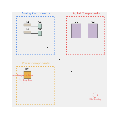
3.3 Wiring and Connections
In the realm of electronic design, wiring and connections form the backbone of any schematic created in OrCAD. Understanding the correct methodologies for wiring is crucial for ensuring that simulations and designs are not only functional but also efficient and reliable. This subsection delves into the intricacies of creating effective wiring connections within OrCAD, emphasizing practical applications, techniques, and common pitfalls.
Wiring Basics in OrCAD
Wiring in OrCAD involves the connection of different components on a schematic, enabling them to interact as intended. Every circuit design begins with the placement of various components, such as resistors, capacitors, and integrated circuits. Once the components are laid out, the next step is to establish connections using the wiring tools available in OrCAD.
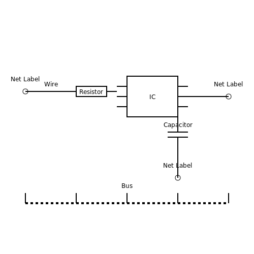
OrCAD provides a straightforward interface for wiring connections, which includes tools for drawing wires, buses for grouping connections, and the ability to create connection points through net labels. Understanding the differences between these tools is essential:
- Wires: Basic connections between two points.
- Buses: Allow multiple wires to be grouped together for better organization and to represent parallel connections.
- Net Labels: Enable the identification of connection points that might not be directly wired but need to establish a logical relationship.
Practical Wiring Techniques
To effectively wire your design in OrCAD, consider the following techniques:
- Efficient Layout: Start by placing components in a logical layout that minimizes crossing wires and allows for straightforward routing. This practice not only aids understanding but also improves signal integrity.
- Utilize Layers: Make use of multiple layers in the PCB layout stage, which can help in keeping power and signal lines separated to minimize interference.
- Consistent Naming: Use descriptive names for your net labels to convey the purpose of each connection, making it clear and understandable for others who might work on the schematic.
Simulating Connections
After establishing your wiring, the next critical step is simulation. OrCAD's simulation tools allow for the verification of circuit behavior before physical implementation. This process encompasses checking for potential logic errors, unintended shorts, and ensuring that components function together as designed.
For simulations, understanding how connections can affect circuit performance is vital. For example, in a voltage divider circuit, the resistance values affect the output voltage significantly. Thus, ensuring precise wiring and component values leads to accurate simulation results.
Common Pitfalls and Solutions
Even experienced users may encounter challenges while making connections in OrCAD. Here are some common issues and their respective solutions:
- Missing Connections: Always verify connections by using the highlight function to check if the nets are properly connected before running simulations.
- Wiring Conflicts: Ensure that wires do not cross unnecessarily. Use buses to organize wires and reduce complexity.
- Incorrect Net Assignments: Double-check net labels to ensure they are correctly applied and reflect the intended connections.
By applying these techniques and being mindful of potential pitfalls, you can create effective, efficient, and accurate schematics that facilitate successful electronics design workflows.
Conclusion
In conclusion, effective wiring and connections within OrCAD not only lay the foundation for functional electronic designs but also enhance the overall efficiency of the design process. Utilizing techniques such as efficient layout, net labeling, and verification through simulation can significantly improve the outcomes of your projects. As you continue using OrCAD, always remember that the quality of wiring directly influences the performance and reliability of the final product.
3.4 Design Rules and Error Checking
In the realm of PCB design, particularly using tools like OrCAD, adherence to design rules and effective error checking is crucial for producing functional, manufacturable boards. As we refine our designs, understanding and applying these principles not only prevents costly mistakes but also enhances the engineering process.
The Importance of Design Rules
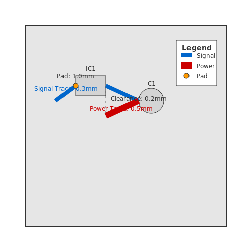
Design rules are a set of guidelines that govern various parameters of the layout, such as trace width, clearance between components, and pad sizes. By implementing these rules, designers ensure that:
- Electrical Integrity: Proper distances and sizes prevent short circuits and ensure signal integrity.
- Manufacturability: Following manufacturer specifications avoids production errors.
- Thermal Management: Adequate spacing and heat dissipation methods mitigate overheating issues.
OrCAD provides a comprehensive framework for defining and enforcing design rules. These rules can be customized for specific projects, taking into account the unique requirements of the circuit being implemented. For example, a high-frequency layout may require tighter impedance control compared to a low-frequency power distribution network.
Error Checking Workflow
An effective design workflow involves continuous error checking throughout the design process. OrCAD integrates several tools for this purpose:
- Electrical Rule Check (ERC): A tool that flags violations regarding the electrical performance of the PCB, such as unconnected nets or mismatched component values.
- Design Rule Check (DRC): Ensures that layout constraints, as defined by the designer, are adhered to. This includes aspects like minimum trace widths and clearance requirements.
- Signal Integrity Analysis: This advanced feature enables designers to predict how signals behave as they traverse the PCB, providing insights on potential issues related to crosstalk and reflection.
The integration of these tools makes error detection and resolution more seamless. For instance, if the DRC flags a clearance violation, OrCAD allows designers to quickly navigate to the problematic area, facilitating rapid diagnosis and correction.
Practical Example: Applying Design Rules
Consider a scenario where you are designing a mixed-signal PCB. Necessary design rules might include:
- A minimum trace width of 10 mils for power traces to support the current load.
- A clearance of at least 6 mils between signal traces to reduce electromagnetic interference (EMI).
- A specific pad size for SMD components to match component specifications accurately.
By specifying these parameters in OrCAD, you can ensure that the design remains within acceptable limits throughout the design cycle.
Conclusion
In summary, the meticulous application of design rules in OrCAD, coupled with robust error-checking mechanisms, is essential for creating reliable, high-quality PCBs. Understanding and leveraging these features not only enhances design efficiency but significantly reduces the chances of costly revisions during production.
4. Understanding PCB Design Flow
4.1 Understanding PCB Design Flow
The PCB design flow is a critical aspect of creating effective electronic circuits and systems. Understanding this flow enhances your ability to create printed circuit boards (PCBs) that not only function correctly but are also manufacturable and reliable. The PCB design process encompasses several key phases that transition from conceptual ideas into tangible, functioning hardware.Conceptualization and Requirements Gathering
The first stage in the PCB design flow involves identifying the project requirements. This includes defining the functionality of the circuit, which components will be utilized, and the electrical specifications such as voltage levels, current capacity, and required frequencies. Advanced engineers often conduct feasibility studies during this phase, analyzing potential constraints around size, power consumption, cost, and thermal management. For instance, in the design of a high-frequency RF circuit, one must consider the effects of parasitics and impedance matching to ensure optimal performance. Integrating these considerations early in the design process leads to fewer iterations and a more efficient workflow.Schematic Capture
Once the concept is established and requirements are collected, the next phase is schematic capture. This process allows designers to create a graphical representation of the electronic circuit using specialized software like OrCAD. During schematic capture, you define the relationships between various components (resistors, capacitors, ICs, etc.) and their connections. Software tools provide libraries of standard components along with the possibility to create custom parts. By utilizing a software-generated netlist, you establish electrical connections that will be integral to the flow of the PCB design.PCB Layout Design
After confirming the schematic, you transition to the PCB layout design phase. This is where the logical design is translated into a physical layout. Here, designers must consider several factors: - Component Placement: Optimal placement helps minimize signal degradation and interference. It is critical to place high-frequency components close together and align components that share power and ground connections effectively. - Routing Paths: Routing involves creating the actual paths for electrical connections on the board. It is essential to follow good design practices such as maintaining the shortest paths, proper trace width for current carrying, and eliminating unnecessary vias. - Layer Management: Advanced PCBs often require multiple layers to accommodate complex layouts without causing interference. Deciding how many layers to use has implications for manufacturing costs and performance. To illustrate, when designing a multilayer PCB for a digital signal processing device, you might use dedicated ground and power planes while distributing the signal traces across the remaining layers to minimize noise.Signal Integrity and Design Rule Check (DRC)
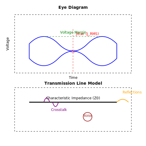
With the layout drafted, it's crucial to perform a Signal Integrity analysis and Design Rule Check (DRC). Simulations can predict issues that might arise during operation, such as crosstalk, noise, and reflections. Advanced tools in OrCAD allow you to perform these simulations to ensure that the design meets performance requirements. DRC is another critical check where the software verifies the layout against predefined rules such as minimum trace widths, spacing rules, and clearance requirements. This step helps to avoid manufacturing defects which can arise from geometry that is too close or too small.Manufacturing Preparation: Gerber Files and Bill of Materials (BOM)
Once the design is validated, the final steps include generating Gerber files and compiling a Bill of Materials (BOM). Gerber files provide a comprehensive description of the different layers of the PCB and are the standard file format used by manufacturers for fabricating the board. A well-prepared BOM lists all required components, including supplier information and part numbers, which facilitate procurement during the manufacturing stage. As illustrated throughout the PCB design flow, each of these phases is interconnected, with decisions made in earlier stages profoundly impacting the efficiency and effectiveness of subsequent steps. Understanding the overall PCB design flow not only enhances your design capabilities but also aligns your approach with best practices seen in industry standards. In conclusion, the PCB design flow in OrCAD is a nuanced and systematic process that integrates theoretical knowledge with practical application. As you advance your skills in PCB design, remember that proficiency comes from iterative practice and continual learning. By honing each stage of this flow, you prepare yourself to tackle increasingly complex electronics challenges in real-world applications.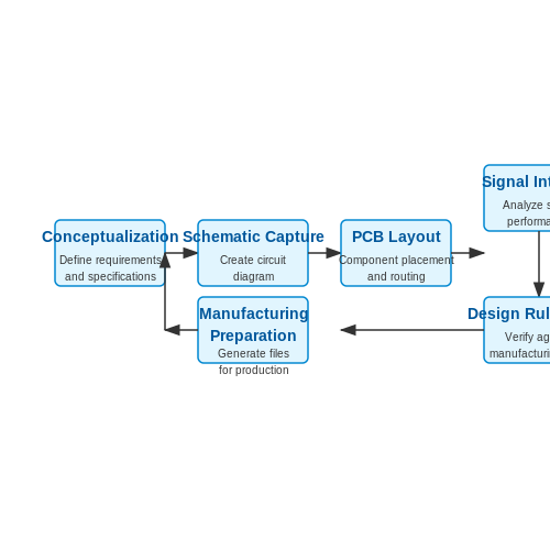
4.2 Importing Schematics into PCB Layout
In the world of electronics design, ensuring a seamless transition from schematic capture to PCB layout is crucial for efficient workflow and reducing errors. The process of importing schematics into a PCB layout environment in OrCAD requires a nuanced understanding of both the software tools available and the underlying principles of circuit design. This subsection delves into the methodologies integral to this process, emphasizing both the technical steps and the broader implications for design integrity.
Understanding the Schematic Design
Before importing the schematic into the PCB layout, it is paramount to validate the schematic design. This involves checking for errors such as unconnected pins, incorrect component values, and violations of design rules. OrCAD's schematic editor provides built-in tools, allowing designers to run electrical rules checks (ERC), which help to identify potential issues prior to import.
The Import Process
Once the schematic is verified, the import process into the PCB layout can commence. This typically involves the following steps:
- Choosing the Right Layout Tool: Ensure that you are using OrCAD PCB Designer or an equivalent layout tool that integrates seamlessly with OrCAD Capture.
- Creating a New PCB Layout: Start a new PCB layout project, ensuring that the board's dimensions accommodate the design requirements.
- Importing the Schematic: Use OrCAD's built-in import feature, typically found under the 'Design' menu. Select the appropriate schematic file you wish to import.
- Component Assignment: Confirm that components in the schematic are correctly linked to the PCB footprint. This can include mapping schematic symbols to the physical outlines in the PCB layout.
- Net Connections: Validate the net connections to ensure that wiring from the schematic accurately reflects on the PCB layout.
Post-Import Validation
After importing, conduct a thorough verification of the layout. This should include:
- Design Rule Check (DRC): This automated check will highlight any discrepancies in trace width, clearance, and layer assignment. Adjust as necessary based on these findings.
- Signal Integrity Analysis: Perform simulations to ensure that routing adheres to high-frequency design considerations, mitigating issues such as crosstalk and signal degradation.
- 3D Visualization: Utilize OrCAD's 3D viewer to inspect the physical layout for misalignments or clearance issues that may not be evident in 2D views.
Conclusion
Success in PCB layout design is heavily reliant on the accuracy of the schematic and the precision of the import process. By adhering to the outlined steps and rigorously validating the design, engineers can significantly enhance the reliability of their electronic products. This meticulous attention to detail not only reduces the time and cost associated with prototyping but also echoes throughout the lifecycle of the device, ensuring performance and durability in real-world applications.
References and Further Reading
- OrCAD PCB Designer — A comprehensive toolset designed for PCB layout, offering advanced features for seamless integration with OrCAD Capture.
- Routing Techniques in CAD — This resource offers insights into effective routing strategies and best practices in PCB design.
- Electronics Tutorials — A platform for educational resources covering various topics in electronics, including PCB design and schematic creation.
- EDA247 - PCB Layout — This site discusses PCB layout guidelines and how to effectively translate schematics into layouts.
- LTSpice for PCB Simulation — A powerful simulator for validating subsystem design, applicable in conjunction with CAD applications.
- Altium Designer Documentation — Extensive documentation on PCB design methodologies, useful for understanding inter-software compatibility.
- NI Multisim — A popular platform for analysis and design that seamlessly integrates with PCB layout software.
4.3 Component Placement Strategies
The effective placement of components within a PCB (Printed Circuit Board) layout is crucial for optimizing performance, manufacturability, and reliability. The strategies employed during the component placement phase have significant implications for signal integrity, electromagnetic interference (EMI), thermal management, and overall design efficiency. This subsection unveils various strategies that engineers should consider while interacting with OrCAD, a robust PCB design tool.
Understanding the Fundamentals of Component Placement
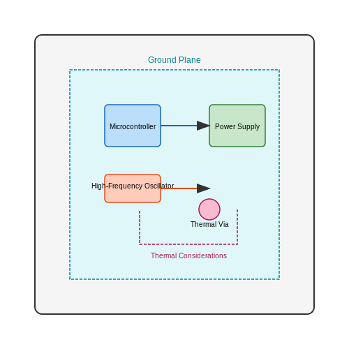
Before diving into specific strategies, it is essential to grasp the fundamental principles affecting component placement. Factors such as signal integrity, thermal dissipation, mechanical assembly, and operational reliability should be evaluated to achieve an optimal design. For example, components responsible for high-speed signals—like microcontrollers and high-frequency oscillators—must be placed in close proximity to minimize trace lengths, which helps reduce inductive and capacitive parasitics.
Strategies for Effective Component Placement
When using OrCAD, several strategies can be effectively implemented for efficient component placement:
- Hierarchical Placement: Begin by organizing components into logical groups based on functionality. For instance, clustering power supply components, signal processing units, and interface circuitry can simplify routing and testing.
- Iterative Optimization: Utilize OrCAD's simulation tools to iterate through different placements and evaluate circuit behavior under varied conditions. Rather than finalizing placements in one go, iterative adjustments can isolate and mitigate performance issues.
- Thermal Management: Pay attention to thermal dissipation, especially for components that generate significant heat. Positioning heat-sensitive components away from high-temperature areas and integrating thermal vias can maintain operational efficiency.
- Ground Planes and Power Distribution: Make use of ground planes to facilitate a low-impedance return path. Position power distribution components to minimize voltage drop and ensure stable operation.
- Use of Design Rules: Leverage OrCAD's design rule checks (DRC) to enforce spacing guidelines and prevent potential fabrication issues before production.
Real-World Applications
To illustrate the significance of these strategies, let’s analyze a case study involving a high-speed digital circuit. In this project, engineers faced challenges with signal integrity due to long trace lengths and proximity to noise sources. Through strategic placements using the hierarchical method, and thermal considerations aided by simulation tools within OrCAD, they effectively reduced signal degradation. Their iterative approach not only improved performance but also streamlined the PCB manufacture, resulting in time and cost savings.
Conclusion
The art of component placement is a blend of science and engineering intuition. Engaging with OrCAD's powerful layout capabilities, guided by effective strategies, can significantly enhance the performance and reliability of electronic circuits. As technology advances, the importance of adopting sophisticated placement strategies will only grow, making it essential for engineers to stay abreast of best practices.
4.4 Routing Techniques and Tools
Routing in PCB design is a critical process that determines how signals, power, and ground connections are formed between various components on a circuit board. Utilizing the right techniques and tools is essential to optimize both the performance and manufacturability of a PCB. In this section, we will explore advanced routing techniques within OrCAD software and the associated tools that facilitate effective PCB layout.
Advanced Routing Techniques
When dealing with PCB routing, it is important to consider various advanced techniques to maximize performance and minimize issues such as interference and signal degradation. Some of the most effective techniques include:
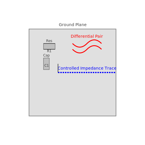
- Controlled Impedance Routing: This technique is crucial when routing high-speed signals. The impedance of a trace can be controlled by adjusting its width, the distance from the reference plane, and the dielectric thickness.
- Differential Pair Routing: Essential for high-frequency signals, differential pairs consist of two traces carrying equal and opposite signals. OrCAD facilitates the routing of differential pairs to ensure they maintain a consistent impedance.
- Teardrop Connection: Using teardrop shapes to connect traces can reduce stress concentrations, particularly at lead connections to pads, enhancing longevity and reliability.
- Ground Planes: Implementing solid ground planes minimizes electromagnetic interference (EMI) and provides a low-resistance path for return currents, critical in high-frequency designs.
Tools for Effective Routing in OrCAD
OrCAD provides a suite of tools that streamline the routing process. Understanding how to leverage these tools can greatly enhance design efficiency.
1. PCB Editor
The PCB Editor in OrCAD offers powerful functionalities such as the ability to auto-route nets, which can save significant time during the layout phase. However, manual adjustments may still be necessary to optimize signal integrity based on the techniques discussed earlier.
2. OrCAD's Constraint Driven Routing
This tool allows the PCB designer to set specific constraints and rules (e.g., width, clearance) for different nets, which ensures that the constraints are respected throughout the routing process. This capability is especially useful for high-speed designs where impedance and other factors must be meticulously managed.
3. DRC (Design Rule Check)
After routing, the DRC functionality is indispensable as it checks for any violations of the established design rules. DRC can automatically highlight issues such as trace clearance violations, width discrepancies, and unwanted overlaps, allowing for immediate correction and validation of the design integrity.
4. Interactive Routing Tools
OrCAD also includes interactive routing tools that offer real-time feedback as changes are made. This feature supports how critical routes can be adjusted dynamically with immediate implications on the overall design — a fluid approach that enhances both creativity and technical precision.
Real-World Applications
Advanced routing techniques and tools are not just theoretical; they find widespread application in sectors such as telecommunications, aerospace, and consumer electronics. For instance, in the aerospace industry, the ramifications of poor routing can lead to catastrophic failures. Therefore, stringent routing practices are not only beneficial but necessary. Meanwhile, consumer electronics production has shifted towards increasingly compact designs, necessitating precise routing methods that maintain performance in smaller form factors.
In summary, mastering the routing techniques and tools provided in OrCAD is essential for advanced PCB design. By applying these methods and leveraging the specific features of OrCAD, engineers ensure that the final product meets both performance standards and manufacturability, paving the way for successful implementation in real-world projects.
4.5 Design Rule Checks (DRC)
In the realm of printed circuit board (PCB) design, the assurance that the final layout adheres to predefined specifications and can effectively function in real-world applications is paramount. This assurance is typically achieved through the use of Design Rule Checks (DRC), an essential feature integrated into OrCAD.
DRC serves as a methodology to automatically validate the layout against defined design rules that correspond to manufacturing capabilities and operational requirements. Before delving into the specifics of DRC within OrCAD, it is critical to understand the fundamental advantages it provides in PCB design.
Understanding Design Rules
Design rules represent a set of criteria that PCB designs must fulfill to ensure manufacturability and reliability. These rules include, but are not limited to:
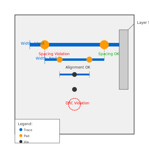
- Spacing Rules: Minimum distances between different conductive traces, pads, and vias.
- Width Rules: Constraints on trace widths that prevent overheating and ensure current-carrying capacity.
- Alignment Rules: Regulations governing how components and pads should be positioned relative to one another.
- Layer Stackup Considerations: Rules pertaining to the arrangement and thickness of each layer in multi-layer PCBs.
By adhering to these rules, designers can mitigate risks of manufacturing defects, enhance performance, and ultimately reduce costs associated with prototype failures.
Setting Up DRC in OrCAD
When you initiate a project in OrCAD, setting up DRC involves configuring the rule set to your specific design requirements. This is typically accomplished in the PCB design software through the following steps:
- Access the DRC Setup Menu: Navigate to the options available under the 'Design' tab and select 'Design Rules' to access the configuration menu.
- Define Rule Parameters: An intuitive interface allows you to define parameters for each rule, including tightness, severity of violations, and specific scenarios requiring relaxation of certain rules.
- Run DRC: Once rules are set, you can execute a DRC scan that identifies any potential design violations.
Visual representations, such as warning symbols or color-coded highlights, will be displayed on the layout, guiding you directly to areas that require correction.
Interpreting DRC Results
Once a DRC scan is completed, the results are presented in a logical manner, allowing for an efficient review. Typically, DRC violations are categorized into warnings, which indicate potential issues that may not necessarily result in failure, and errors, which signify critical violations that must be rectified before proceeding to manufacturing.
The DRC report generated by OrCAD provides details on each violation, including:
- The type of rule breached.
- The specific location of the violation within the PCB design.
- Recommendations for resolving the issue.
Practical Implications of Effective DRC
The implications of effectively utilizing DRC in OrCAD extend beyond mere compliance; they fundamentally impact product quality, performance, and time-to-market:
- Quality Control: By catching errors early in the design phase, the likelihood of manufacturing defects is significantly reduced.
- Cost Efficiency: Minimizing rework and scrappage leads to substantial savings, particularly in production environments.
- Enhanced Reliability: Following strict design rules helps ensure that the electrical and thermal performance of components conforms to expectations, bolstering reliability in end applications.
Ultimately, the integration of DRC practices into your PCB design workflow will empower you to produce robust and reliable designs that meet both customer needs and industry standards.
In conclusion, mastering DRC processes within OrCAD is critical for any advanced-level engineer or designer, requiring an intimate understanding of rule configurations, interpretation of results, and the implications of design corrections. As the complexity of electronic devices continues to escalate, so too does the necessity for sophisticated design checks, making DRC an invaluable tool in the electronic design automation suite.
5. Setting Up Simulations
5.1 Setting Up Simulations
In the realm of electronic design automation (EDA), OrCAD stands out as an invaluable tool for engineers and researchers seeking to simulate various circuit designs. To achieve credible simulations, meticulous attention to setup detail is paramount. This section delves into the intricate steps necessary to establish simulations effectively, focusing on OrCAD's capabilities and ensuring accurate results.
Understanding Simulation Types
The simulation process encompasses various techniques, each tailored for specific analyses. The primary types of simulations utilized in OrCAD include:
- Transient Analysis: This simulation examines circuit behavior over time, allowing users to visualize voltage, current, and power waveforms as they change dynamically.
- AC Analysis: Essential for understanding the frequency response of a circuit, this analysis evaluates how circuits respond to sinusoidal inputs across a range of frequencies.
- DC Sweep Analysis: This type assesses how circuit parameters vary with differing DC input conditions, crucial for finding operating points and conduction regions.
Preparing the Circuit in OrCAD
Before diving into simulation, the circuit must be meticulously crafted within OrCAD's schematic environment. Ensure that all components are appropriately defined, connected, and that necessary values (like resistor values or capacitor specifications) are set. It is also imperative to confirm that the simulation profile aligns with the type of analysis you intend to execute.
For example, in a transient simulation, voltage sources should be defined to behave as impulse inputs to observe their impact on circuit dynamics. This highlights the significance of appropriate setup, as misconfigurations could lead to inconclusive or false results.
Configuration of Simulation Parameters
Once the schematic is appropriately defined, the next essential step involves configuring simulation parameters. In OrCAD, this can be initiated by accessing the Simulation settings through the toolbar. Key parameters to specify include:
- Simulation Time: For transient simulations, defining the total time and time step is crucial to capturing dynamic behaviors accurately.
- Analysis Type: This needs to correspond with the focus of your circuit analysis, whether beam analysis, noise analysis, etc.
- Initial Conditions: In many cases, initial voltage or current conditions may need to be specified to ensure realistic behavior during the simulation.
Let’s configure a simple transient analysis simulation:
This equation portrays the voltage across a capacitor charging over time, where \( V_0 \) is the maximum voltage, and \( \tau \) is the time constant. In OrCAD, you would set these parameters accordingly, aligning your circuit components with expected theoretical values.
Running the Simulation
After all parameters are set, you can kick-off the simulation by selecting 'Run' from the Simulation tool menu. During this process, monitoring tools within OrCAD permit real-time observation of ongoing simulations, enabling immediate feedback. Graphical outputs, such as waveform displays, can provide intuitive insights into circuit behavior, revealing parameters such as rise times, settling times, and nominal steady-state voltages.
It is advisable to analyze results critically, often comparing simulated data to theoretical predictions or values obtained through experimental measurements. Discrepancies can highlight potential errors in circuit design or misconfigurations in the simulation settings.
Post-Simulation Analysis
Upon successful completion of the simulation, OrCAD allows for detailed inspection of results through plotting and parameter selection tools. Graphical representations facilitate examination patterns within the circuit outputs. Employing these tools effectively means being able to draw conclusions or make design modifications based on empirical evidence obtained from simulations.
In summary, setting up simulations in OrCAD involves a structured approach of defining the circuit, selecting the appropriate simulation parameters, executing the simulation, and thoroughly analyzing the results. Mastery of this process not only enhances design efficiency but also mitigates risks associated with circuit failures in real-world applications.
5.2 Types of Analysis Available
In modern electronic design automation (EDA), tools like OrCAD provide a comprehensive suite of analysis capabilities that enable engineers and researchers to predict circuit performance, validate designs, and mitigate risks before physical implementation. Understanding the various types of analysis available in OrCAD can significantly enhance the design process and lead to more reliable and cost-effective solutions.
OrCAD facilitates several types of analyses, each serving distinct functions and providing insights relevant to different stages of circuit design. This section will cover the most prominent types of analyses and their implications in practical scenarios.
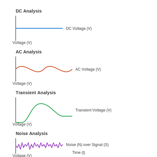
DC Analysis
DC analysis, or Direct Current analysis, is fundamental in assessing the steady-state behavior of circuits. This analysis focuses on determining the voltages and currents in a circuit when all time-varying signals have settled to constant levels. Knowledge of DC operating points is crucial for biasing transistors and ensuring proper function in analog applications.
The mathematical foundation for DC analysis can be articulated through Kirchhoff’s laws. Kirchhoff's Voltage Law (KVL) states that the sum of the electrical potential differences (voltage) around any closed circuit is zero. This can be expressed as:
For a simple circuit, we can apply KVL to calculate node voltages and branch currents consistently, leading to a robust design verification process.
AC Analysis
AC analysis extends the principles of DC analysis into the realm of alternating current signals. It is essential for understanding how circuits respond to sinusoidal inputs at various frequencies. This analysis utilizes phasor transformations, converting differential equations into algebraic ones, thus simplifying calculations involving reactive components.
The transfer function, a key concept in AC analysis, captures the relationship between the input and output of the circuit as:
where \(s\) is the complex frequency variable. Engineers can manipulate this function to evaluate gain, phase shift, and bandwidth, compelling features in RF design and filtering applications.
Transient Analysis
Transient analysis is crucial for observing how a circuit reacts over time to changes in inputs, such as switching actions, step functions, or pulse inputs. This analysis captures the dynamic behavior, providing insights into timing and stability. With accurate models of capacitance and inductance, engineers can predict ringing, overshoot, and settling times.
The differential equations governing transient responses are typically derived from the governing laws of circuits, creating a comprehensive depiction of how voltages and currents evolve with respect to time. For example, the charging of a capacitor in an RC circuit can be modeled as:
This equation characterizes the voltage across the capacitor as it charges, displaying the interaction between resistance (R), capacitance (C), and time (t).
Noise Analysis
In practical circuits, noise can significantly affect performance, especially in sensitive applications such as amplifiers and signal processing systems. Noise analysis assesses the impact of various noise sources, quantifying how they influence signal integrity.
This type of analysis often involves calculating parameters like Signal-to-Noise Ratio (SNR) and Total Noise Figure (NF), which can be expressed mathematically as:
By simulating noise under different conditions, engineers can design robust filters and optimize components to minimize undesired interference.
Monte Carlo Analysis
Monte Carlo analysis applies statistical methods to account for component tolerances and variations in manufacturing processes. By simulating numerous iterations of circuit behavior with varying parameters, it enables designers to predict the likelihood of failure and enhance reliability.
The probabilistic nature of this analysis allows engineers to visualize distributions of outputs rather than just average values, providing a deeper understanding of the design's robustness. This analysis is especially pertinent in systems where precision is critical, such as in aerospace and medical devices.
Conclusion
In summary, OrCAD equips users with a robust set of analytical tools for conducting diverse analyses: DC, AC, transient, noise, and Monte Carlo analyses each play pivotal roles in ensuring the success of electronic prototypes and products. Mastery of these analyses not only facilitates effective circuit verification but also enhances the overall design strategy, minimizing cost and time associated with physical prototyping.
5.3 Interpreting Simulation Results
In applied electronics design, simulations serve as crucial testing grounds to validate circuit behavior before implementation. The validation of these simulations becomes paramount as it can avert costly errors in real-world applications. As we delve into interpreting simulation results, it's essential to establish a solid foundation that will enable us to effectively translate numerical outputs into practical insights.Understanding Simulation Outputs
When we conduct simulations using OrCAD, the results manifest in various forms: voltage waveforms, current responses, and transient behavior over time. Extracting actionable conclusions from these results requires a keen understanding of what these datasets signify in the context of the circuit's design and operation.Voltage and Current Waveforms
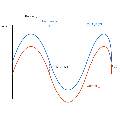
Voltage and current waveforms are fundamental outputs that present the dynamics of electrical signals through components. Typically illustrated in graphical format, these waveforms reveal vital behaviors of the circuit, including peak values, RMS values, and phase relationships. For example, a standard voltage waveform may be displayed with both amplitude and time scaled on the axes. The interpretation involves identifying key characteristics such as:- Peak Voltage: Indicates the maximum voltage the circuit experiences, essential for component ratings.
- Frequency: Crucial for filters and oscillators, indicating how quickly the waveform oscillates.
- Phase Shift: Particularly important in AC circuits, reflecting how voltage and current relate to one another.
Transients and Steady-State Analysis
Transitions from one state to another—transient analysis—provide insights into circuit behavior during switch operations or sudden input changes. The importance of analyzing transients lies in the evaluation of circuit stability and performance under dynamic conditions. On the other hand, steady-state analysis focuses on how the circuit behaves under constant conditions over time. It becomes critical in power distribution and communication designs, where consistent performance is desired. During transient analysis, one may observe the time constant, given by the equation:Invalid Assumptions and Model Limitations
While OrCAD provides robust simulation tools, it's essential to remain aware of the limitations and assumptions that accompany the models. Factors such as parasitic elements, non-ideal components, and environmental conditions may skew results. For instance, models for operational amplifiers may not account for bandwidth limitations, leading to overconfidence in circuit performance. Taking care to compare simulation results with theoretical predictions—and understanding the variances—will enhance the learning process. Implementing a feedback loop through post-simulation analysis allows for iterative improvements to design and validation, ensuring each revision approaches better fidelity with real-world results.Practical Applications
The process of interpreting simulation results goes beyond theory; it has myriad practical applications across industries. Engineers utilize OrCAD simulations for tasks such as:- Design Verification: Ensuring that new designs perform according to specification before physical prototyping.
- Fault Analysis: Running simulations to identify potentially problematic components under various operating scenarios.
- Performance Optimization: Utilizing insights gained from simulation to adjust component values and improve efficiency.
5.4 Troubleshooting Common Simulation Issues
In the realm of electronic design automation (EDA), effective simulation is crucial for verifying the functionality and performance of circuits before actual prototyping. However, users of OrCAD, like any complex tool, may encounter simulation issues. Understanding these problems, their origins, and solutions is essential for any engineer or researcher looking to streamline their workflow and ensure accurate results.
Understanding Simulation Errors
Common simulation errors often stem from a variety of sources, including component models, configuration settings, and convergence issues. Recognizing the type of error is the first step towards mitigation. Error types can generally be categorized into:
- Model Errors: These arise when the defined parameters of components do not accurately represent real-world behavior.
- Convergence Errors: These occur when the simulator cannot find a consistent solution across the time steps.
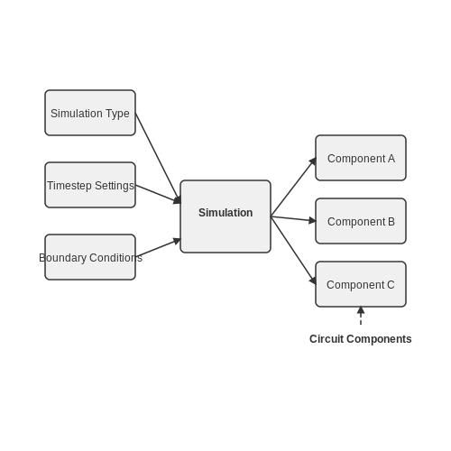
- Configuration Errors: These stem from incorrect setup in the simulation parameters, such as inadequate timestep settings or boundary conditions.
Identifying Model Errors
Model errors can manifest as incorrect outputs, simulation crashes, or unrealistic behavior in the circuit. One common approach to troubleshoot these is to verify the models used in the simulation. Ensure that each component in your schematic has an appropriate model assigned. You may consult the OrCAD model library to find verified models or consider creating custom models if needed.
Additionally, run simulations on simpler circuits to isolate problems. If a complex design fails, start building your circuit incrementally to identify at what stage issues arise.
Tackling Convergence Issues
Convergence issues may yield "non-convergence" errors or lead to simulations that hang indefinitely. Start by checking if your circuit is properly biased—this is crucial for circuits involving inductors and capacitors. Adjust your simulation settings by employing different convergence algorithms in OrCAD or altering solver options.
Increasing the time step or decreasing the simulation time can sometimes yield results. Moreover, introducing small resistance in parallel with capacitors (often termed as “initial biasing”) can help the simulator find a solution more effectively.
In this equation, if a circuit does not have sufficient resistive paths, it can lead to convergence accuracy issues due to floating voltages or undefined states. Adequate practices involve providing a definite path for current to facilitate simulation stability.
Resolving Configuration Issues
Configuration issues typically arise when the simulation environment does not correlate with the intended design objectives. Pay close attention to:
- Simulation Type: Ensure that you are using the correct simulation type for your analysis needs (e.g., transient, AC, DC).
- Timestep Settings: Adjust your timestep settings depending on the dynamics of the circuit. High-frequency circuits generally require smaller timesteps.
- Boundary Conditions: Make certain that any load or source termination is appropriate for your simulation.
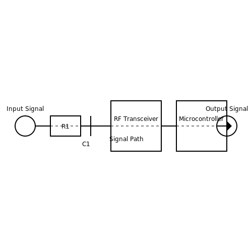
To visualize these configurations more effectively, consider using a block diagram representation of your settings, illustrating how each component interacts within the simulation environment. This approach allows for more straightforward debugging and a clearer understanding of potential pitfalls.
Practical Relevance and Case Studies
Real-world applications of troubleshooting in OrCAD often manifest during the design verification phases of projects. For instance, in automotive electronics, ensuring that simulation results are comparable to actual performance can lead to significant safety and performance benefits. A documented case study by a leading automotive manufacturer highlights how resolving convergence issues early in the design process saved substantial costs related to late-stage modifications.
In conclusion, simulation issues in OrCAD are often systematic and can be appropriately addressed through methodical testing and adjustment. By employing strategic troubleshooting, engineers can mitigate risks, ensuring robust design verification and ultimately facilitating smoother transitions from simulated environments to physical implementations.
6. Creating Bill of Materials (BOM)
6.1 Creating Bill of Materials (BOM)
In the realm of electronics design, particularly when utilizing OrCAD, the creation of a Bill of Materials (BOM) is not only a procedural necessity but also a strategic approach to ensure comprehensive documentation of components and materials involved in a project. A well-structured BOM serves as a critical part of the design workflow, linking design files with manufacturing and procurement processes.
The BOM is essentially a detailed list of raw materials, components, assemblies, sub-assemblies, parts, and quantities required to manufacture a product. From electronic circuits to complex devices, a BOM enables engineers to maintain clarity and organization throughout the design and production stages. This process involves several steps, each contributing to the accuracy and functionality of the final product.
Understanding the BOM Structure
A typical BOM can be structured into several levels, which may include:
- Header Section: This contains essential information such as the project name, revision number, and creation date.
- Itemized List: Each entry describes a unique component or assembly, providing details such as part number, description, quantity, and supplier information.
- Associated Documentation: References to schematics, layout files, and assembly processes that correspond to each item.
Designers often categorize components based on various criteria, including but not limited to, type (e.g., resistors, capacitors, ICs), function (e.g., passive vs. active), and sourcing (e.g., standard components vs. custom parts). This categorization not only helps in better management but also streamlines sourcing and inventory processes.
Generating a BOM in OrCAD
OrCAD provides a robust platform for creating a BOM from your schematic designs seamlessly. To generate a BOM, you typically follow these steps:
- Design your Circuit: Start by designing your circuit in OrCAD Capture, ensuring accuracy in component placement and connections.
- Assign Attributes: Right-click on components to review and edit attributes like part number, description, and parameters necessary for creating a comprehensive BOM.
- Run the BOM Report: Navigate to the Report menu, select ‘Bill of Material’ from the list, and specify the configuration according to your project’s requirements.
Upon execution, OrCAD generates the BOM tailored to the specified layout, allowing you to customize the output format as needed (such as CSV, Excel, etc.). This feature is essential, given the diverse needs of procurement, manufacturing, and logistics teams.
Practical Relevance
In practice, creating an accurate and well-documented BOM not only minimizes errors during assembly but also aids in sourcing and inventory control. Engineers are increasingly recognizing its importance in optimizing production workflows and contributing to the overall success of the project lifecycle.
For instance, a case study involving the development of a complex medical device illustrated how discrepancies in BOM entries led to sourcing delays, ultimately affecting the project's timeline. By utilizing a structured approach to BOM generation in OrCAD, the design team was able to establish a clear communication channel between engineering and procurement, ensuring timely availability of all components.
In conclusion, a well-crafted BOM offers clarity and efficiency in electronic design, serving as a foundation for successful product realization. Leaning on the capabilities of OrCAD, engineers can navigate the complexities of modern electronic assembly with greater assurance and efficacy.
6.2 Exporting Gerber Files
In the realm of printed circuit board (PCB) design, the ability to export Gerber files is paramount. Gerber files are essential for the manufacturing process, as they contain the design data that guides the production of each layer of the PCB. Understanding the intricacies involved in exporting these files can significantly influence both the efficiency and accuracy of your PCB projects. To comprehend the significance of Gerber files, we must first recognize their role as the primary set of instructions that communicate a designer's specifications to PCB manufacturers. Each Gerber file corresponds to a specific layer of the PCB — for instance, the copper layers, silkscreen, solder mask, and mechanical outlines. Moreover, the sophistication of modern PCB designs often means that your Gerber files will need to adhere to specific manufacturing capabilities and standards to ensure that your design is realized as intended.Understanding the Gerber Format
The Gerber format, primarily derived from the RS-274-D standard, provides a vector graphic format for precisely defining geometrical shapes on each layer of a PCB. Each file typically includes detailed information regarding the layout, apertures for pads, traces, and other features paramount for manufacturing. The latest iteration, RS-274X, adds additional features such as the inclusion of aperture definitions directly within the files, streamlining data exchange between designers and manufacturers. To successfully export your PCB designs into the Gerber format using OrCAD, one must follow several crucial steps to ensure all necessary data is accurately captured. Failure to include particular files or layers can result in costly manufacturing delays or, worse, defective products.Steps for Exporting Gerber Files in OrCAD
1. Preparing the Design: Before initiating the export process, ensure that your PCB design is complete and free of errors. Utilize the Design Rule Check (DRC) tool available in OrCAD to identify and rectify any potential issues. 2. Accessing the Export Options: Navigate to the "File" menu in OrCAD and select "Export". From the submenu, choose "Gerber". This selection will lead you to the Gerber export settings. 3. Configuring Gerber Options: Here, you will be presented with various options. Key settings to consider include: - Layer Selection: Specify which layers to export (e.g., top copper, bottom copper, silkscreen). - Units: Ensure the correct unit of measurement (inches or millimeters) is selected. - Aperture Settings: Choose the desired aperture format to ensure compatibility with the manufacturing processes. 4. Verifying Output Files: After configuring the options, OrCAD will generate a preview of the Gerber files. Review this preview to ensure all components and layers are accurately represented. 5. Exporting the Files: Once the inspection is satisfactory, choose the destination directory and initiate the export. Upon completion, a set of Gerber files will be created, ready for submission to your PCB manufacturer. 6. Post-Export Validation: It is prudent to validate the exported Gerber files using a Gerber viewer. This step serves as a final check to prevent any potential manufacturing issues.Practical Considerations in Gerber File Management
In a professional setting, maintaining an organized folder structure for Gerber files can enhance workflow efficiency. Additionally, consider implementing a version control system to track design changes, safeguarding against miscommunication with PCB fabricators. The process of exporting Gerber files, while straightforward, demands attention to detail and an understanding of manufacturing standards. Each step, from preparation to post-export validation, bears significance in realizing your PCB designs successfully. By mastering these techniques, engineers and designers can contribute to seamless transitions from concept to production, minimizing errors and optimizing project timelines. In conclusion, exporting Gerber files is not merely a technical task; it is an essential bridge between design innovation and practical implementation. As you delve deeper into the world of PCB design, let this knowledge of exporting processes serve as a foundation for robust and efficient manufacturing practices.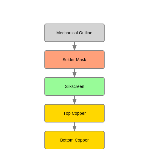
6.3 Preparing Documentation for Manufacturing
When transitioning from design to production, high-quality documentation is crucial. This documentation not only serves as a blueprint for manufacturing but also ensures that all teams involved—from engineering to marketing—are aligned with the specifications and functionalities of the final product. In this section, we will explore the steps and considerations necessary for preparing comprehensive manufacturing documentation using OrCAD.
Understanding the Role of Documentation in Manufacturing
Manufacturing documentation acts as the backbone for any electronic product, detailing every aspect required for production. This encompasses schematic diagrams, layout designs, and assembly instructions. Well-prepared documentation can significantly enhance manufacturing efficiency, reduce errors, and improve communication among stakeholders.
Key Components of Manufacturing Documentation
To effectively prepare documentation in OrCAD, focus on the following key components:
- Schematic Diagrams: These documents illustrate the electrical connections and components of the circuit design. Ensure that the schematic representation is clear and adheres to industry standards to facilitate understanding and verification.
- PCB Layouts: Each layout must be detailed, specifying layer stack-ups, trace widths, and pad sizes. This information is vital for fabricating the printed circuit boards (PCBs) accurately.
- Bill of Materials (BOM): A comprehensive BOM lists all components required for production, including part numbers, quantities, and suppliers. Each entry should be accurate to prevent supply chain disruptions.
- Assembly Instructions: Providing clear instructions for assembling the product can streamline the integration of various components, minimizing assembly errors. Include visual aids when possible to enhance clarity.
- Testing Procedures: Documentation should outline the necessary tests to ensure that the finished product meets design specifications. This may include functional tests, thermal tests, and reliability assessments.
Generating Documentation in OrCAD
OrCAD provides various tools to generate the necessary documentation for manufacturing. To create effective documentation:
- Utilize the Design Rule Check (DRC): This feature ensures that the designed circuit adheres to specified constraints, reducing potential issues during manufacturing.
- Export Functional Schematic: Once your schematic is complete, export it as a PDF or in a vector format, ensuring that it is easily readable and correctly labeled.
- Create the PCB Layout: Use OrCAD to produce Gerber files, which are the standard for PCB manufacturing. These files include all crucial information regarding layer patterns and drilling specifications.
- Compile the BOM: Use OrCAD’s BOM tool to pull component data and format it appropriately. Make sure to cross-verify part compatibility and availability from suppliers.
Review and Verification
Before finalizing the documentation, conducting a thorough review is essential. This involves validating all aspects of the documentation with stakeholders, including engineers, product managers, and manufacturing partners. Misinformation at this stage can lead to costly delays and production errors.
Incorporating a feedback loop during reviews helps gather insights and make necessary adjustments, ultimately leading to a more robust manufacturing process. An up-to-date repository of documentation also benefits ongoing maintenance and future product iterations.
Conclusion
In the realm of electronics design, meticulous documentation preparation is pivotal for ensuring a smooth transition to manufacturing. Advanced tools within OrCAD allow engineers to produce comprehensive, accurate documents needed to guide the manufacturing process. By emphasizing the key components of manufacturing documentation and validating them through stakeholder engagement, organizations can greatly enhance their production efficacy and product quality.
By implementing these best practices, you can ensure that your designs not only perform well in simulations but also translate seamlessly into real-world applications.
7. Design Reuse and Libraries Management
7.1 Design Reuse and Libraries Management
In the realm of electronic design automation (EDA), the significance of design reuse and effective libraries management cannot be overstated. As designs become more complex, the need to optimize design cycles, minimize errors, and leverage existing resources is paramount. This section delves into the various strategies, methodologies, and practical applications of design reuse within OrCAD, highlighting how engineers can harness libraries to enhance productivity and ensure consistency across projects.
Understanding Design Reuse
Design reuse involves the strategic application of existing design elements, components, and architectures in new projects. This practice not only accelerates the design process but also enables engineers to capitalize on previously validated designs, thereby reducing the likelihood of errors. Considerable time savings are achievable through this method, particularly when combined with a robust library management system.
In practical terms, design reuse often involves:
- Component Reuse: Utilizing previously designed components transparently in new projects.
- Configuration Management: Keeping track of variations and revisions to ensure consistency across designs.
- Standardization: Implementing standard components allows for simplified integrations and checks.
OrCAD Libraries: Structure and Management
Within OrCAD, effective library management can make or break a project's success. Libraries house components and their associated data, including electrical characteristics and footprint information. A well-organized library structure facilitates efficient design reuse. This section accrues several best practices in managing libraries effectively:
1. Categorization and Structuring
Organizing components into meaningful categories is essential. A hierarchical structure, where components are grouped by type, function, or project, optimizes retrieval times. For example, components can be divided into analog, digital, and mixed-signal categories, allowing for quick access during the design phase.
2. Version Control
Version control is critical in environments where designs evolve rapidly. Implementing a versioning system within your libraries ensures that engineers can track changes. OrCAD provides capabilities that allow for the management of multiple versions of a component, ensuring that any design can revert to previous iterations if necessary.
3. Component Validation and Updates
To ensure reliability, components in libraries must be validated regularly against industry standards. Automatic updates, if configured properly within OrCAD, can alert engineers to changes in component specifications or new best practices. Conducting periodic reviews keeps libraries relevant and usable in modern applications.
Real-World Application: A Case Study
To illustrate the practical relevance of design reuse and libraries management, let's consider a case study in a mid-sized electronics firm that specializes in consumer electronics. The company faced challenges in meeting tight product release schedules due to redundant design efforts. By implementing a centralized library system within OrCAD and promoting a culture of design reuse, the design department achieved a 40% reduction in development time over one year.
This was accomplished through:
- Standardizing designs for frequently used components.
- Encouraging engineers to document and share design choices for future reuse.
- Integrating a real-time collaboration platform where changes in libraries were instantly updated across the teams.
Adhering to structured design reuse protocols not only enhanced productivity but also improved the quality and reliability of final products, cementing the workflow's efficacy.
As we move forward in this tutorial, understanding the implications of libraries and design reuse will lay the groundwork for more complex topics, such as the integration of simulation tools and hardware design practices in OrCAD.
7.2 Custom Component Creation
The design of electronic circuits often necessitates the use of components that are not readily available in commercial libraries. In these instances, the ability to create custom components in OrCAD becomes invaluable. This subsection delves into the nuances of custom component creation, providing a systematic approach to designing, modeling, and implementing unique electronic components.Understanding Component Creation in OrCAD
Custom components in OrCAD consist of both schematic symbols and layout footprints. A schematic symbol is the graphical representation of the component used in design schematics, while the footprint refers to the physical attributes of the component for PCB layout. Understanding these two aspects is crucial in ensuring the component functions accurately within a broader circuit design. The initial step in custom component creation encompasses identifying the parameters and specifications that the component must adhere to, such as operating voltage, current ratings, and pin configurations. Advanced users often utilize both the OrCAD Capture and OrCAD PCB Designer environments to foster a smooth transition between schematic design and PCB layout.Creating Schematic Symbols
To create a schematic symbol, start by launching OrCAD Capture and navigating to the library where the new component will be stored. Follow these steps: 1. Open the Library Editor: Select 'File' -> 'New' -> 'Library.' This initiates a new library for your custom components. 2. Create a Symbol: Use the 'Place' menu to select 'Part,' enter the required parameters for your new component, and define the pin layout. Ensure that the pin numbering corresponds to the physical layout to prevent connectivity issues during simulation and testing. 3. Define Electrical Properties: Assign necessary electrical parameters to each pin, such as input/output status and electrical connections. It is beneficial to have access to the component specifications provided by manufacturers, as this information will guide the accurate definition of the component's physical and electrical characteristics.Designing the Layout Footprint
Once the schematic symbol has been created, the next phase is to design the corresponding footprint in OrCAD PCB Designer. Here, precision is essential. The layout needs to align well with the pin-outs defined in the schematic. 1. Access the PCB Editor: Click on 'File' -> 'New' -> 'Footprint.' 2. Define Pad Size and Shape: Specify the pad dimensions based on the recommended design guidelines provided by the component manufacturer. This typically includes hole size, pad shape (round or square), and pad spacing. 3. Place Pads and Outline: Position the pads according to the schematic symbol defined earlier. Ensure that the silkscreen layer is also represented to avoid confusion during assembly. Careful attention to the footprint design will facilitate better manufacturability of the PCB and ensure reliable connections for the custom component when evaluated in real-world applications.Validation and Simulation
After creating both the schematic symbol and footprint, the component must undergo validation. OrCAD provides tools for this purpose, enabling users to simulate the component within the context of a larger circuit. Validation checks ensure compliance with the specifications and functionality of the designed component. Additionally, employing Monte Carlo simulations or worst-case scenario analyses can help to analyze potential variances in application circumstances, assisting engineers in fine-tuning their designs. In practice, custom components are frequently used in industries such as telecommunications, medical electronics, and consumer gadgets where specific requirements cannot be fulfilled by off-the-shelf components. Such bespoke creations not only enhance circuit customization but also improve performance optimized to meet exact criteria. Creating custom components in OrCAD is a critical skill for engineers and designers who seek greater control over their electronic designs. The steps outlined provide a framework from which advanced users can develop precision components tailored to specific applications, ensuring both effectiveness and reliability in circuit design.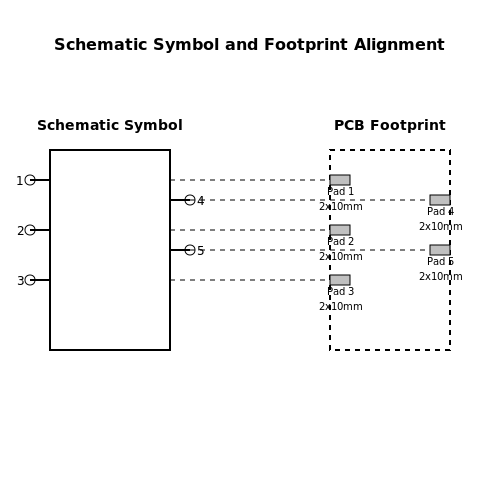
7.3 Utilizing OrCAD with PLM Software
Integration of OrCAD, a powerful suite for electronic design automation (EDA), with Product Lifecycle Management (PLM) software can greatly enhance the management of electronic design data. Engineers and researchers often face the need to streamline their workflows, enhance collaboration, and ensure that all changes to designs and components are consistently handled. This section explores the synergistic relationship between OrCAD and PLM software, focusing on methods for effective utilization and the advantages of such integration.
Understanding PLM in the Context of EDA
To appreciate the benefits of integrating OrCAD with PLM systems, it is essential to understand the role that PLM plays in product development. PLM acts as a comprehensive framework that manages the lifecycle of a product from inception, through engineering design and manufacturing, to service and disposal. By incorporating electronic design data into PLM systems, organizations can ensure:
- Version Control: Maintained and accessible records of all design iterations, crucial for auditing and compliance.
- Collaboration: Enhanced communication among interdisciplinary teams, ensuring that designers, engineers, and project managers all have access to the latest data.
- Data Integrity: Consistent use of data models and specifications across the organization, reducing errors and redundancy.
In many organizations, integrating OrCAD with PLM systems can mitigate the challenges faced in managing large datasets produced during the design process. Tools like OrCAD enable designers to create, simulate, and analyze complex electronic systems while PLM software keeps track of related documentation, tools, and assets. This dual functionality forms a robust foundation for effective product development.
Implementation Strategies
The implementation of OrCAD in conjunction with PLM software requires careful planning and execution. Here are some steps and considerations for effective integration:
- Identify Critical Integration Points: Determine which data sets should flow between OrCAD and the PLM system. Commonly, schematic designs, component libraries, and manufacturing data are critical.
- Use APIs and Data Interfaces: Leverage the application programming interfaces (APIs) provided by both OrCAD and PLM software. These APIs can facilitate the automated transfer of design data into PLM systems. This reduces manual input and the risk of human error.
- Establish Change Management Protocols: Implement workflows that manage how changes are tracked and approved within the PLM system. This ensures that all stakeholders are informed of significant design modifications.
- Training and Skill Development: Ensure that teams are adequately trained to use both OrCAD and the PLM system. This may involve workshops or training sessions focusing on data management and integration procedures.
Real-World Applications
Numerous industries, including automotive, aerospace, and consumer electronics, have benefited from the integration of OrCAD with PLM systems. For instance, the automotive industry utilizes rigorous PLM solutions to manage complex electronic components in vehicles. By integrating OrCAD within these systems, companies can ensure compliance with stringent regulations and safety standards, while drastically reducing time-to-market.
A historical case study highlighting the effectiveness of this integration involves a major electronics manufacturer that faced inconsistencies in its design processes. By implementing PLM and integrating it with OrCAD, the company reported a 40% reduction in design cycle time and significantly improved error tracking, leading to a sharper competitive edge in the market.
Overall, the fusion of OrCAD and PLM systems exemplifies how advanced engineering tools can be harnessed to optimize workflows, enhance collaboration, and maintain data integrity throughout the product lifecycle. This not only streamlines the design process but also fosters innovation and supports the dynamic needs of evolving industries.
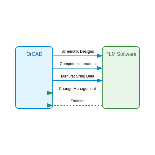
8. Common Setup Issues
8.1 Common Setup Issues
In the realm of circuit simulation and design, OrCAD serves as a robust platform widely utilized by engineers and researchers alike. While the software boasts impressive functionality, it is not without its challenges during setup and operation. This section delves into the common setup issues faced by users, aiming to equip you with the knowledge needed to troubleshoot these challenges effectively.
Licensing Issues
One of the most frequent challenges encountered when setting up OrCAD is related to licensing. Ensuring that the software is correctly licensed is crucial, since a missing or incorrect license can lead to several operational limitations. Users often face issues such as:
- The software not starting due to an invalid license key.
- License server communication problems, which may stem from network configuration.
- Expired licenses that require renewal.
To address licensing issues, always verify the license against the requirements specified by your organization and check server configurations if you are using a network license.
Installation Errors
Installation errors can stem from a variety of sources, including system incompatibility and user access privileges. Common manifestations include:
- Failure to install due to an unsupported operating system version.
- Permissions errors that impede the installation process, often requiring administrative access.
For a smooth installation, ensure that your system meets the software requirements and run the installation file as an administrator.
Configuration of Libraries and Components
An effective design in OrCAD relies heavily on correctly configured libraries and components. Users may encounter issues such as missing parts or incompatible library files. This often manifests in error messages during simulation, indicating:
- Missing component models, hindering simulation and design verification.
- Incompatibility with current project settings.
To resolve these issues, it is imperative to verify the library paths used within your projects. Ensure that all required libraries are properly installed and linked within the OrCAD environment.
Network and Connectivity Issues
For users working in collaborative environments, network connectivity problems can pose significant challenges. Issues may include:
- Inability to connect to shared libraries or components.
- Slow performance due to bandwidth limitations.
Assess your network connection and consider utilizing local copies of frequently used libraries to enhance performance and reduce dependency on real-time network accessibility.
Simulation Settings and Parameters
Users often face difficulties with simulation settings, leading to incorrect results or failed runs. Common pitfalls include:
- Default simulation parameters that may not be suitable for the current project.
- Improper setup of analysis types, such as transient vs. steady-state conditions.
Prior to running simulations, review the project settings thoroughly. Adjust parameters to match the specific requirements of the circuit being designed.
Conclusion
Navigating OrCAD's setup challenges requires a mixture of technical knowledge and troubleshooting skills. By familiarizing yourself with the common issues discussed in this section, you can streamline your process and mitigate losses in productivity.
8.2 Error Messages and Solutions
In the world of electronic design automation, specifically within the capabilities of OrCAD, engineers often encounter a myriad of error messages that can disrupt workflows and lead to ineffective designs. Understanding these error messages and having strategies to address them is crucial for maintaining efficiency and productivity.Common Types of Error Messages
Error messages in OrCAD primarily fall into three broad categories: design rule violations, simulation errors, and library issues. Each type serves as a warning or a signal that an aspect of the design must be revised or corrected to meet specific criteria.- Design Rule Violations: These occur when the layout or schematic does not comply with predefined design rules. Issues can include trace spacing that is too narrow or component placement that breaches clearance specifications.
- Simulation Errors: Errors arising from simulations often indicate problems with the model parameters, circuit connections, or simulation settings. They can lead to failed simulations that hinder analysis.
- Library Issues: Missing or incorrect library references can result in inability to find components or incorrect values being used in simulations.
Addressing Design Rule Violations
Design rule violations often manifest during the physical layout phase of a project. When encountering an error message such as "Trace Width Too Narrow," it is essential to understand the underlying rules defined in the design settings. To rectify this, one should: 1. Check the design rule settings in OrCAD to ensure they reflect the requirements of the intended fabrication process. 2. Use the “Design Rule Check” (DRC) feature to identify specific locations causing the problem. 3. Adjust the trace widths or spacing accordingly, followed by re-running the DRC to validate compliance. By following this systematic approach, you can iteratively resolve most design rule issues, ensuring that your layout adheres to the necessary standards.Resolving Simulation Errors
Simulation errors can be particularly perplexing due to their dependency on various factors ranging from incorrect input parameters to connection errors. A common error might state "The simulation failed due to discontinuous behavior." To solve this, consider the following steps: 1. Review the convergence settings and modify parameters such as time step or maximum iteration limits. 2. Examine component values; ensure they are realistic and appropriate for the working conditions. 3. Double-check the connectivity in your schematic, as incorrect connections can lead to unexpected simulation results. Understanding the underlying physics of the simulation will guide you in diagnosing problems effectively. For example, recognizing that a failed simulation could often indicate instability in the circuit, as opposed to merely mechanical error, can prevent unnecessary troubleshooting.Correcting Library Issues
Library issues often emerge when components are improperly defined or when libraries themselves are missing. The error message “Library Not Found” is prevalent in scenarios where different versions or repositories are in use. To address library issues: 1. Ensure that the library paths are correctly set. This can be done under the settings/preferences in OrCAD. 2. Validate component definitions to ascertain they live up to expected attributes, parameters, and values. 3. Regularly update your libraries to include the latest components and configurations. Regular library maintenance and verification will prevent many avoidable library-related errors.Conclusion
Dealing with error messages in OrCAD can be daunting, yet it serves as an opportunity to refine your design skills and enhance your knowledge of electronic circuit design processes. By breaking down these messages, addressing the root causes, and employing systematic troubleshooting strategies, you can turn potential setbacks into valuable learning experiences. Thus, not only do you resolve current issues, but you also build a more robust foundation for future designs and simulations.8.3 FAQs and Best Practices
For professionals engaging with OrCAD, addressing common questions and adhering to best practices is vital for effective design and simulation. This section delves into frequently asked questions along with practical strategies and methodologies to enhance the application of OrCAD for PCB design and simulation.Frequently Asked Questions
1. What are the primary features of OrCAD that differentiate it from other design software?
OrCAD stands out with its comprehensive set of tools, which include schematic capture, PCB layout, signal integrity analysis, and thermal analysis. Its integration with Allegro facilitates advanced simulation capabilities, making it suitable for complex projects.2. How can I optimize simulation time in OrCAD?
To enhance simulation efficiency, ensure that your model accuracy is balanced with simulation speed. Techniques include simplifying models, reducing mesh size in simulations, and leveraging OrCAD's SmartView feature, which allows for a quicker overview of data without requiring full simulation.3. Can OrCAD handle mixed-signal designs?
Yes, OrCAD supports mixed-signal design environments. Utilizing OrCAD PSpice allows for the simulation of both digital and analog components in a single environment, which is invaluable for designs that incorporate both domains.4. What libraries should I use for common components?
Utilizing well-maintained component libraries significantly increases your design efficiency. OrCAD provides a robust library manager, and sources like the Ultra Librarian and Digi-Key’s component libraries can be used to access thousands of up-to-date component models.Best Practices for Using OrCAD
1. Organize your Design Files
Maintaining an organized structure for your design files can significantly ease collaboration and troubleshooting. Use a logical directory structure for projects, and ensure consistent naming conventions for schematic files, footprints, and models.2. Validate Design Rules Regularly
Utilize OrCAD’s Design Rule Check (DRC) frequently throughout the design process. This proactive approach helps identify errors early, minimizing the risk of costly redesigns. Engaging the DRC ensures conformity with manufacturing specifications and improves reliability.3. Implement Version Control
Employ a version control system such as Git to manage changes within your projects. This reduces the risk of data loss and supports collaborative efforts across teams. Ensure that backups are performed regularly to safeguard against unforeseen errors.4. Use Simulation Effectively
Leverage OrCAD's extensive simulation capabilities early in the design phase. By validating electrical performance through simulations such as transient analysis, you can identify potential problems before moving to physical prototyping, thereby saving time and resources.5. Document Your Design Choices
Thorough documentation of your design and analysis process is critical. This serves as a guide for others who may work on the project in the future and enhances understanding of design decisions. Documentation can also help in compliance with industry standards. In conclusion, a mastery of OrCAD’s features coupled with best practices can lead to significantly improved efficiency and innovation in your design projects. The synthesis of advanced tools and disciplined practices positions engineers and researchers to push the boundaries in electronics design effectively.9. Recommended Books on OrCAD
9.1 Recommended Books on OrCAD
- Learn OrCAD PSpice and PCB Design Full Edition — This book by Marc E. Herniter provides a comprehensive guide to OrCAD, covering both fundamental and advanced concepts in PSpice and PCB design. It includes practical examples and detailed explanations to assist with real-world applications.
- Complete PCB Design Using OrCAD Capture and PCB Editor — Written by Kraig Mitzner, this resource offers a step-by-step approach to PCB design using OrCAD Capture. Ideal for both beginners and advanced users, it provides a thorough understanding of the software's capabilities.
- Circuit Design and Simulation with OrCAD Capture and PSpice — This text by Denis Fitzpatrick is aimed at academics and professionals who wish to deepen their knowledge of circuit design, simulation, and implementation using OrCAD tools, including PSpice.
- PSpice for Circuit Analysis and Design — Authored by Paul W. Tuinenga, this book is an excellent primer for anyone needing to master circuit simulations with PSpice, offering clear explanations and practical insights into the modeling fundamentals.
- Simulation and Analysis of Modern Electric Systems — This book by Hector J. Altuve Ferrer explores advanced simulation techniques using PSpice with practical case studies focused on modern electric systems, making it beneficial for engineers and professionals in the field.
- Analog Circuit Design: A Tutorial Guide to Applications and Solutions — Robert Pease provides a detailed tutorial on analog circuit design, leveraging OrCAD tools for enhanced simulation solutions. The book includes practical advice and problem-solving techniques relevant to circuit designers.
- Getting Started with OrCAD — A Step-by-Step Approach — This resource by Bruce Carter guides readers through the initial stages of using OrCAD, with detailed examples and step-by-step instructions useful for both students and professionals wanting to integrate OrCAD into their workflows.
9.2 Online Resources and Tutorials
In the realm of advanced electronics design, OrCAD serves as a powerful tool for engineers and researchers. Optimizing your proficiency with OrCAD requires a mixture of theoretical knowledge and practical experience. In this subsection, we delve into high-quality online resources and tutorials that cater to advanced learners looking to refine their skills and broaden their understanding. The importance of staying updated with the latest tools and practices in electronics design dictates that these resources should be both current and comprehensive.
Exploring these resources will help you to not only capitalize on OrCAD's technical capabilities but also to understand the latest advancements in electronics design. This collection of resources includes diverse formats such as video tutorials, scholarly articles, community forums, and specialized blogs. Each resource is chosen for its depth and relevance to advanced topics in electronics design using OrCAD.
- Cadence: OrCAD Training — Offers immersive training modules that cover a wide spectrum of OrCAD functionalities, ideal for honing specialized skills in circuit design and simulation.
- Altium Library — Although primarily focused on Altium Designer, it offers comparative insights and best practices that can be applied to OrCAD design processes.
- OrCAD Journals — A compilation of articles and case studies addressing advanced OrCAD techniques and their applications in various fields of electronics.
- LinkedIn Learning: OrCAD Courses — Features video-led courses designed for professionals aiming to expand their knowledge in specific OrCAD modules and improve their design capabilities.
- Microchip Developer Help — Contains extensive documentation and tutorials on circuit design procedures which can be transposed into OrCAD environments for efficiency.
- YouTube: Circuit Design Tutorials — Provides video guides covering advanced OrCAD features, structured to help experienced users tackle complex design challenges.
- EDABoard OrCAD Forum — A community-driven platform where advanced users share solutions, discuss updates, and collaborate on challenging OrCAD problems.
- PCB Expert: OrCAD PCB Design Tips — Offers insights and practical tips from industry experts, focused on optimizing PCB designs with OrCAD.
By leveraging these resources, advanced users can refine their application of OrCAD in real-world scenarios, staying adapted to the rapid advancements in electronic design technologies. Whether seeking in-depth tutorials or community support, these sources ensure a comprehensive progression in skill and knowledge.
9.3 Communities and Forums
In the diverse landscape of circuit design and simulation, OrCAD stands out as a comprehensive tool suite utilized by professionals for PCB design, schematic capture, and simulation. However, even seasoned experts occasionally face challenges that require insight beyond the documentation. This is where communities and forums play an indispensable role. They provide platforms for engineers, physicists, and researchers to exchange ideas, solve complex problems, and keep up with the latest innovations in the field.
Importance of Online Communities in Learning and Problem-Solving
For advanced users of OrCAD, participating in online communities is not just about receiving assistance; it's a two-way street that enhances collective knowledge. These communities foster a collaborative environment where:
- Knowledge Sharing: Experts share innovative solutions, best practices, and application tips that are not typically covered in official resources.
- Real-time Problem Solving: Swift responses from peers who may have encountered similar technical issues.
- Networking Opportunities: Building connections with fellow professionals can lead to collaborative projects or career prospects.
Types of Communities and Their Offerings
Applied OrCAD users can access a myriad of online platforms, each offering unique benefits. Here are some common types of communities:
1. Official Cadence Community
As the official community for Cadence products, including OrCAD, it offers:
- Dedicated Forums: Subforums for different OrCAD components like PCB Editor, which aid in focused discussions.
- Technical Articles: Insights provided directly by Cadence experts that may cover unique use-cases or advanced techniques.
2. Edaboard and Similar Forums
These platforms offer a broader community of electronics enthusiasts and professionals:
- Diverse User Base: Users here often bridge gaps between theoretical understanding and practical application across various EDA tools.
- Extensive Archives: Older threads can provide surprisingly relevant insights or solutions that are applicable to new problems.
Additional Resources for In-Depth Learning
To maximize the potential of OrCAD, users should explore not only focused forums but any resource offering in-depth knowledge. Here is a mix of online assets to enrich your understanding:
- PSpice Forum — An active forum dedicated to PSpice users within OrCAD, providing a venue for technical discourse on simulation intricacies.
- Reddit Electronics — A vibrant community where numerous electronics topics, including OrCAD, receive attention from cross-disciplinary participants.
- Mentor Community — Often frequented by electronic design veterans, this is a space to compare OrCAD to other tools, understanding competitive advantages.
- Element14 Community — Offers comprehensive content, from technical blogs to webinar series, often showcasing how tools like OrCAD can be applied in innovative ways.
- Electronics Stack Exchange — A rigorous Q&A platform where high-quality questions and answers about OrCAD and related engineering challenges are shared.
- EE Times — Provides news, articles, and seminars on the latest developments in electronics, complementing in-depth technical insights with industry trends.
Engaging with these communities not only aids in overcoming immediate technical hurdles but also elevates your proficiency in utilizing OrCAD for complex design projects. By being an active member, you contribute to the broader dialogue that accelerates innovation and excellence in electronic design automation.