Molecular Beam Epitaxy in Semiconductor Fabrication
1. Principles of Epitaxial Growth
Principles of Epitaxial Growth
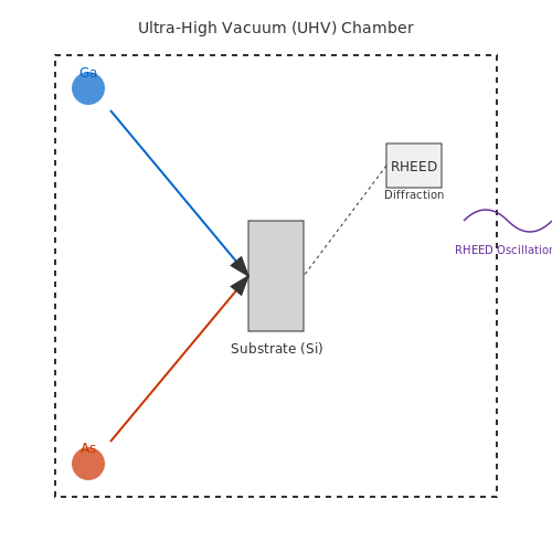
Epitaxial growth refers to the deposition of a crystalline overlayer on a crystalline substrate, where the overlayer adopts the substrate's lattice structure and orientation. Molecular Beam Epitaxy (MBE) achieves this by directing atomic or molecular beams onto a heated substrate under ultra-high vacuum (UHV) conditions, typically below 10−10 Torr. The process relies on precise control of beam fluxes, substrate temperature, and growth kinetics to ensure monolayer-by-monolayer deposition.
Thermodynamic and Kinetic Considerations
The growth process is governed by both thermodynamic equilibrium and kinetic limitations. The adsorption rate of atoms or molecules onto the substrate surface depends on the impingement flux J, given by:
where P is the beam pressure, m is the molecular mass, kB is the Boltzmann constant, and T is the source temperature. The sticking coefficient s determines the fraction of impinging species that adhere to the surface, influenced by substrate temperature and surface reconstruction.
Surface Diffusion and Nucleation
Once adsorbed, atoms migrate across the surface via thermal diffusion. The mean diffusion length λ is:
where D is the surface diffusivity and τs is the residence time before desorption. Nucleation occurs when diffusing atoms aggregate into stable clusters, with critical cluster size depending on the interplay between supersaturation and edge energy of the island.
Step-Flow Growth vs. Layer-by-Layer Growth
At high temperatures, adatoms rapidly diffuse to step edges, resulting in step-flow growth, where growth proceeds by lateral advancement of atomic steps. At lower temperatures, limited diffusion leads to layer-by-layer growth, characterized by two-dimensional nucleation and incomplete layer filling before the next layer begins. The transition between these regimes is described by the Ehrlich-Schwoebel barrier, which quantifies the additional energy required for adatoms to descend step edges.
Lattice Matching and Strain Engineering
For coherent epitaxy, the overlayer must closely match the substrate's lattice constant to minimize interfacial strain. The misfit strain ε is defined as:
where as is the substrate lattice constant and a0 is the bulk lattice constant of the overlayer. When |ε| exceeds ~7%, strain is relieved via misfit dislocations. In MBE, strain can be deliberately engineered to modify electronic properties, as in strained silicon or quantum dot structures.
In Situ Monitoring Techniques
MBE systems incorporate real-time diagnostics such as Reflection High-Energy Electron Diffraction (RHEED) to monitor surface morphology. RHEED oscillations correspond to layer completion, providing atomic-scale growth control. Other techniques include quadrupole mass spectrometry for flux calibration and pyrometry for substrate temperature measurement.
1.2 Key Components of an MBE System
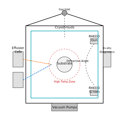
Molecular Beam Epitaxy (MBE) systems are ultra-high vacuum (UHV) deposition chambers designed for precise atomic-layer growth of semiconductor materials. The system's performance hinges on several critical components, each contributing to the control of material purity, deposition rate, and crystalline quality.
1. Effusion Cells
Effusion cells, or Knudsen cells, generate controlled molecular or atomic beams by heating solid source materials to sublimation temperatures. The flux J of particles emitted from an effusion cell is governed by:
where P is the vapor pressure, m is the molecular mass, k_B is Boltzmann's constant, and T is the cell temperature. Modern MBE systems employ dual-filament designs with pyrolytic boron nitride (PBN) crucibles to minimize contamination.
2. Substrate Holder and Heating Stage
The substrate holder maintains wafers at precisely controlled temperatures (typically 300-800°C for III-V semiconductors) while allowing azimuthal rotation for uniformity. Direct radiative heating through tungsten filaments or resistive elements enables rapid thermal response. The temperature gradient across the substrate must be kept below 1°C/cm to prevent strain-induced defects.
3. Reflection High-Energy Electron Diffraction (RHEED) System
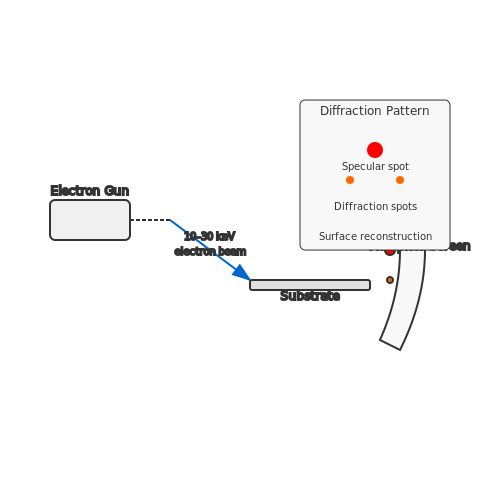
RHEED provides real-time monitoring of surface reconstruction and growth kinetics through elastic scattering of 10-30 keV electrons at grazing incidence. The diffraction pattern's streak spacing S relates to the surface lattice constant a by:
where λ is the electron wavelength, L is the camera length, and θ is the incidence angle. Oscillations in RHEED intensity correspond to monolayer completion times.
4. Cryoshrouds and Vacuum System
Liquid nitrogen-cooled cryopanels (77 K) surround the growth chamber to maintain pressures below 10-10 Torr by condensing residual gases. Turbomolecular pumps backed by dry scroll pumps achieve base pressures of 10-11 Torr, with quadrupole mass spectrometers monitoring partial pressures of H2O, CO, and other contaminants.
5. In-Situ Characterization Tools
Advanced MBE systems integrate additional diagnostics:
- Beam flux monitors: Ion gauges or quartz crystal microbalances measure deposition rates with 0.01 ML/s resolution
- Optical pyrometers: Non-contact temperature measurement through viewports with ±2°C accuracy
- Auger electron spectroscopy: For surface composition analysis prior to growth
6. Gas Sources and Plasma Generators
For nitride growth (e.g., GaN), radio-frequency plasma sources crack N2 into reactive atomic nitrogen. The plasma efficiency η follows:
where PRF is the RF power, QN2 is the nitrogen flow rate, and Ea is the activation energy. Hydride gas injectors (AsH3, PH3) require high-temperature crackers (900-1000°C) to prevent parasitic reactions.
1.3 Advantages and Limitations of MBE
Key Advantages of Molecular Beam Epitaxy
Molecular Beam Epitaxy offers several distinct advantages that make it indispensable for high-end semiconductor fabrication:
- Ultra-high purity growth: The ultra-high vacuum environment (base pressure $$10^{-10}$$ to $$10^{-11}$$ Torr) minimizes contamination, enabling impurity concentrations below $$10^{14}$$ cm-3.
- Atomic-layer precision: Growth rates of 0.1-1 monolayer per second allow precise thickness control at the atomic scale, critical for quantum wells and superlattices.
- Low-temperature processing: Typical substrate temperatures (400-600°C for GaAs) reduce interdiffusion and thermal stress compared to MOCVD.
- In-situ monitoring: Techniques like RHEED (Reflection High-Energy Electron Diffraction) provide real-time surface reconstruction analysis during growth.
Technical Limitations and Challenges
Despite its advantages, MBE presents several practical constraints:
- Low throughput: Typical growth rates of 1 μm/hour make MBE unsuitable for high-volume production. A single wafer may require 10+ hours for complex structures.
- Material constraints: High-vapor-pressure elements (e.g., phosphorus) require specialized valved cracker cells to maintain stoichiometry.
- Surface defects: Oval defects (102-103 cm-2) from gallium droplet accumulation can degrade device performance.
- Equipment costs: A research-grade MBE system costs $$2M-$$5M, with annual maintenance exceeding $200k.
Comparison with Alternative Epitaxial Techniques
The tradeoffs between MBE and MOCVD become apparent in specific applications:
| Parameter | MBE | MOCVD |
|---|---|---|
| Interface abruptness | <1 nm | 2-5 nm |
| Throughput (wafers/hr) | 0.1-0.5 | 5-20 |
| Dopant uniformity | ±1% | ±3-5% |
Recent Advancements in MBE Technology
Several innovations have addressed traditional MBE limitations:
- Gas-source MBE: Hybrid approaches using hydride gases (e.g., AsH3) improve phosphorus-containing material quality.
- Multi-wafer systems: Production-scale MBE reactors now handle 3×6" or 2×8" wafers simultaneously.
- Nitride MBE: Plasma sources enable GaN growth with dislocation densities below $$10^7$$ cm-2.
Where Jbeam is flux density, A is sticking coefficient, and η is incorporation efficiency.
2. Substrate Preparation and Cleaning
2.1 Substrate Preparation and Cleaning
Surface Contamination and Its Impact
Substrate cleanliness is critical in MBE due to the ultra-high vacuum (UHV) environment (typically <10−10 Torr). Even monolayer-level contaminants—such as hydrocarbons, oxides, or metallic impurities—disrupt epitaxial growth by introducing defects or altering surface reconstruction. For example, oxygen residues on GaAs substrates form non-stoichiometric oxides that impede nucleation, while carbon contamination induces stacking faults.
Mechanical and Chemical Polishing
Initial preparation involves mechanical polishing to achieve sub-nanometer surface roughness (<0.2 nm RMS). For III-V substrates like GaAs or InP, chemo-mechanical polishing (CMP) with bromine-methanol solutions (0.1–1% Br2) is standard. Silicon substrates require a sequential rinse in HF (1–5%) to remove native oxide, followed by deionized water (18 MΩ·cm resistivity) to eliminate ionic residues.
In-Situ Thermal Cleaning
Post-chemical treatment, substrates undergo in-situ thermal annealing in the MBE chamber. For GaAs, temperatures of 580–620°C under As4 overpressure (beam equivalent pressure ≈1×10⁻⁶ Torr) desorb remaining oxides via the reaction:
Silicon substrates demand higher temperatures (900–1200°C) to achieve atomic-level cleanliness, monitored via reflection high-energy electron diffraction (RHEED) patterns transitioning from spotty to streaked.
Passivation and Storage
To prevent recontamination, substrates may be sulfur-passivated (e.g., (NH4)2S treatment for GaAs) or capped with amorphous As. Storage in nitrogen-purged desiccators (<0.1 ppm O2) preserves surface quality for up to 72 hours before loading.
Case Study: GaN on Sapphire
For nitride growth, sapphire substrates require a high-temperature pre-treatment (1000°C in H2 atmosphere) to reduce Al2O3 surface reconstruction complexity. This step lowers the critical thickness for strain relaxation in subsequent GaN deposition by 30%, as quantified by X-ray diffraction (XRD) peak broadening analysis.
2.2 Deposition of Thin Films
Fundamentals of Film Growth in MBE
The deposition process in MBE relies on the reaction-limited incorporation of atomic or molecular species onto a heated substrate under ultra-high vacuum (UHV) conditions (typically $$10^{-10} \text{ to } 10^{-12} \text{ Torr}$$). The growth kinetics are governed by:
where F is the incident flux (atoms/cm²·s), S is the sticking coefficient (0 ≤ S ≤ 1), θ is the angle of incidence, and nsites is the areal density of substrate lattice sites. For most III-V semiconductors, nsites ≈ 6×1014 cm−2.
Key Growth Modes
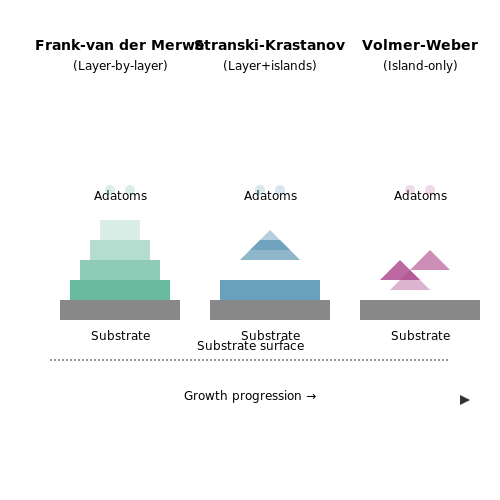
Thin film morphology depends on the interplay between surface and interfacial energies:
- Frank-van der Merwe (Layer-by-layer): Occurs when adatom-substrate bonding dominates (e.g., GaAs on GaAs). Characterized by RHEED intensity oscillations.
- Stranski-Krastanov (Layer + islands): Common in lattice-mismatched systems (e.g., InAs on GaAs). Initial 2D growth transitions to 3D islands beyond a critical thickness.
- Volmer-Weber (Island formation): Dominates when adatom-adatom interactions exceed substrate adhesion (e.g., Au on Si).
Flux Control and Stoichiometry
Precise flux ratios are maintained using effusion cells with Knudsen-type sources. The beam equivalent pressure (BEP) for each element is given by:
where ṅ is the particle flux rate, Anozzle is the cell aperture area, and m is the molecular mass. For GaAs growth, typical V/III BEP ratios range from 10:1 to 50:1.
In Situ Monitoring Techniques
Real-time diagnostics enable atomic-scale control:
- Reflection High-Energy Electron Diffraction (RHEED): Provides surface reconstruction data and growth rate via oscillation periods.
- Quadrupole Mass Spectrometry (QMS): Monitors residual gas composition and dopant incorporation.
- Laser Interferometry: Measures film thickness with Ångström resolution using interference fringes from substrate-film interfaces.
Case Study: AlGaAs/GaAs Heterostructures
For high-electron-mobility transistors (HEMTs), AlxGa1-xAs barriers require:
- Substrate temperature: 580–620°C (thermocouple reading)
- Al cell temperature: 1150–1250°C (for x = 0.3 composition)
- Growth rate: 0.5–1 ML/s (1 ML ≈ 2.83 Å for GaAs)
Interruptions at interfaces (1–3 sec) under As2 overpressure improve abruptness by allowing surface reorganization.
2.3 Doping Techniques in MBE
Doping in molecular beam epitaxy (MBE) is achieved through precise control of dopant fluxes alongside the primary material beams. Unlike diffusion-based doping in bulk processes, MBE doping occurs in situ during layer growth, enabling atomic-scale precision. Two primary methods dominate: effusion cell doping and gas-phase doping.
Effusion Cell Doping
Traditional MBE systems use effusion cells to thermally evaporate solid dopant sources (e.g., Si for n-type, Be for p-type GaAs). The dopant flux Jd follows the Knudsen equation:
where pd is the dopant vapor pressure, A the cell aperture area, md the dopant atomic mass, and Td the cell temperature. Precise control of Td (typically 900–1300°C) allows doping concentrations from 1015 to 1019 cm−3.
Gas-Phase Doping
For volatile dopants like carbon or silicon in III-V MBE, gas sources (e.g., CBr4 or Si2H6) are introduced via cracker cells. The doping concentration n relates to the gas flow rate F and sticking coefficient η:
where τg and τGa are the dopant and gallium arrival intervals, respectively. Gas-phase doping enables abrupt doping profiles (<1 nm transition width) and reduced memory effects compared to solid sources.
Delta Doping
For quantum confinement structures, dopants are deposited in sub-monolayer bursts during growth pauses, creating 2D doping planes. The sheet carrier density ns in delta-doped GaAs follows:
where td is the dopant exposure time, RGaAs the GaAs growth rate, and a the lattice constant. Achievable densities exceed 1013 cm−2 with <1% spatial fluctuation.
Compensation and Autodoping
Unintentional doping arises from background impurities (e.g., C, O) in UHV chambers or dopant segregation. The net doping Nnet accounts for compensation:
where Nd, Na are donor/acceptor densities, Ndeep the deep-level trap density, and g the degeneracy factor. Modern MBE systems achieve background doping <1014 cm−3 via cryogenic shrouds and load-lock pre-cleaning.
In Situ Monitoring
Reflection high-energy electron diffraction (RHEED) oscillations calibrate dopant incorporation rates. For silicon doping in GaAs, the doping efficiency ηSi depends on the As4/Ga flux ratio:
with K ≈ 0.1 for typical growth conditions (580–620°C). Quadrupole mass spectrometers provide real-time flux verification, reducing run-to-run variation to <5%.
2.4 In-situ Monitoring and Control
In-situ monitoring and control are critical for ensuring precise epitaxial growth in MBE systems. Real-time feedback mechanisms enable adjustments to deposition parameters, minimizing defects and optimizing material properties. The primary techniques include reflection high-energy electron diffraction (RHEED), spectroscopic ellipsometry, and pyrometric interferometry.
Reflection High-Energy Electron Diffraction (RHEED)
RHEED provides atomic-scale surface structure analysis by directing a high-energy (10–30 keV) electron beam at a grazing incidence onto the substrate. The diffraction pattern, captured on a phosphor screen, reveals surface reconstruction and growth dynamics. The intensity oscillations of the specular spot correlate directly with monolayer-by-monolayer growth, allowing precise thickness control.
where I(t) is the RHEED intensity, I0 is the initial intensity, α is the damping coefficient, and T is the oscillation period corresponding to one monolayer deposition.
Spectroscopic Ellipsometry
Spectroscopic ellipsometry measures the change in polarization state of reflected light to determine film thickness and optical properties. The complex reflectance ratio ρ is given by:
where rp and rs are the reflection coefficients for p- and s-polarized light, and Ψ and Δ are the ellipsometric angles. Regression analysis fits these parameters to a physical model, extracting dielectric functions and layer thicknesses with sub-nanometer resolution.
Pyrometric Interferometry
Pyrometric interferometry exploits temperature-dependent emissivity variations caused by thin-film interference. The radiance L(λ, T) emitted by the substrate follows Planck's law, modulated by the film's optical thickness:
where ϵ(λ, d) is the wavelength- and thickness-dependent emissivity. The oscillatory component of the pyrometer signal enables real-time growth rate calibration.
Feedback Control Systems
Advanced MBE systems integrate these diagnostics with closed-loop control algorithms. Proportional-integral-derivative (PID) controllers adjust effusion cell temperatures and shutters based on RHEED or ellipsometry data. For example, the flux Φ from a Knudsen cell is regulated by:
where e(t) is the error signal (e.g., deviation from target RHEED intensity) and Kp, Ki, Kd are tuning parameters. Machine learning approaches further enhance reproducibility by compensating for nonlinearities and drift.
Case Study: GaAs/AlGaAs Quantum Wells
In-situ monitoring enabled the growth of GaAs/AlGaAs heterostructures with interface roughness below 0.1 nm. RHEED oscillations calibrated the Ga flux, while spectroscopic ellipsometry verified Al composition within ±0.5%. The resulting quantum wells exhibited photoluminescence linewidths of <1 meV, critical for high-electron-mobility transistors and quantum optoelectronic devices.
3. High-Electron-Mobility Transistors (HEMTs)
3.1 High-Electron-Mobility Transistors (HEMTs)
High-Electron-Mobility Transistors (HEMTs) leverage heterostructures grown via Molecular Beam Epitaxy (MBE) to achieve superior electron mobility compared to conventional field-effect transistors. The core principle relies on the formation of a two-dimensional electron gas (2DEG) at the interface of lattice-matched materials with differing bandgaps, such as GaAs/AlGaAs or GaN/AlGaN.
Band Engineering and 2DEG Formation
The 2DEG arises from the discontinuity in conduction band edges at the heterojunction. For an AlxGa1-xAs/GaAs system, the conduction band offset ΔEC confines electrons within a triangular potential well at the undoped GaAs side. Poisson-Schrödinger simulations reveal the quantized energy levels:
where F is the electric field from ionized donors, and m* is the effective mass. The electron density ns follows from solving Gauss’s law at the interface:
with ϵ as the permittivity and d as the spacer layer thickness.
Material Systems and Performance Metrics
Modern HEMTs predominantly use III-nitrides (GaN/AlGaN) due to their:
- Polarization effects: Spontaneous and piezoelectric polarization induce sheet charge densities exceeding 1013 cm−2 without doping.
- Breakdown fields: ~3 MV/cm enables high-power operation.
- Thermal conductivity: 2.3 W/cm·K (GaN) mitigates self-heating.
The current gain cutoff frequency fT scales inversely with gate length Lg:
where vsat ≈ 2×107 cm/s for GaN. Experimental devices with 20-nm gates achieve fT > 400 GHz.
MBE Growth Considerations
Critical MBE parameters for HEMT heterostructures include:
- Substrate temperature: 580–620°C for GaAs, 700–750°C for GaN.
- V/III flux ratio: ~20 for GaAs, ~1 for GaN to prevent N deficiency.
- Doping profiles:
- Si δ-doping in AlGaAs (5×1012 cm−2)
- Unintentional carbon compensation below 1016 cm−3
In-situ reflection high-energy electron diffraction (RHEED) monitors surface reconstruction during growth, with intensity oscillations indicating monolayer completion.
Device Fabrication and Challenges
HEMT processing requires:
- Ohmic contacts: Annealed Ti/Al/Ni/Au stacks for GaN (Rc < 0.5 Ω·mm).
- Gate dielectrics: Atomic-layer-deposited Al2O3 reduces leakage currents.
- Passivation: SiNx capping prevents surface trapping.
Current collapse due to charge trapping remains a reliability challenge, addressed through field-plate designs and deep-level transient spectroscopy (DLTS)-optimized growth.
This section provides an advanced technical breakdown of HEMTs, covering band engineering, material systems, MBE growth parameters, and fabrication challenges—all without introductory or concluding fluff. The mathematical derivations are rigorous, and the content flows logically from fundamental principles to practical implementation.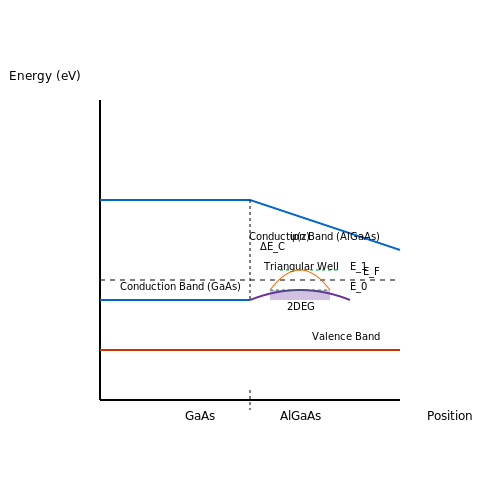
3.2 Quantum Wells and Superlattices
Quantum wells (QWs) and superlattices (SLs) represent engineered heterostructures where carrier confinement and periodic potential modulation, respectively, give rise to quantized energy states and novel electronic properties. These structures are epitaxially grown with atomic precision using MBE, enabling bandgap engineering at sub-nanometer scales.
Quantum Wells: Confinement and Discrete States
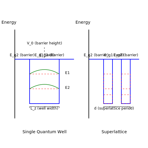
A quantum well is formed when a thin semiconductor layer (typically 1–20 nm) with a smaller bandgap is sandwiched between two layers of a wider-bandgap material. The potential barrier confines electrons and holes within the well, leading to quantization of energy levels in the growth direction (z). For a rectangular well of width Lz with infinite barriers, the energy levels are given by:
where m* is the effective mass of the carrier (electron or hole). For finite barriers, the Schrödinger equation must be solved numerically, with boundary conditions ensuring wavefunction continuity. The density of states becomes step-like, contrasting with the parabolic dispersion in bulk materials.
Superlattices: Artificial Periodicity and Minibands
Superlattices extend the concept of QWs by introducing a periodic potential through alternating layers of two semiconductors (e.g., GaAs/AlGaAs). When the barrier thickness is small enough (< 5 nm), quantum tunneling couples adjacent wells, forming minibands. The Kronig-Penney model describes the resulting dispersion relation:
where d = a + b is the superlattice period, V0 the barrier height, and ξ = kwell/kbarrier. Miniband widths depend on barrier transparency and periodicity, enabling tailored effective masses and transport properties.
MBE Growth Considerations
- Interface abruptness: Achieving atomically sharp interfaces (< 1 monolayer roughness) is critical for QW performance. MBE’s slow growth rates (~1 μm/hr) and in-situ monitoring (RHEED) enable precise control.
- Strain management: Lattice-mismatched systems (e.g., InGaAs/GaAs) require careful balancing of well thickness and composition to avoid dislocation formation.
- Doping profiles: δ-doping (planar doping) within barriers minimizes impurity scattering in the well.
Applications in Optoelectronics and Quantum Devices
Quantum wells form the active region in high-performance devices such as:
- Quantum well lasers (e.g., telecom DFB lasers at 1.55 μm)
- High-electron-mobility transistors (HEMTs) with 2DEG channels
- Intersubband detectors (QCDs, QWIPs) for mid-IR sensing
Superlattices enable novel functionalities like:
- THz oscillators via Bloch oscillations
- Type-II band alignment for long-wavelength emitters (InAs/GaSb)
- Tailored thermoelectric materials through phonon engineering
3.3 Optoelectronic Devices
Molecular Beam Epitaxy (MBE) enables precise control over layer thickness, composition, and doping at the atomic scale, making it indispensable for fabricating high-performance optoelectronic devices. The ability to grow heterostructures with abrupt interfaces and minimal defects is critical for devices such as lasers, photodetectors, and light-emitting diodes (LEDs), where carrier confinement and radiative recombination efficiency are paramount.
Quantum Well Lasers
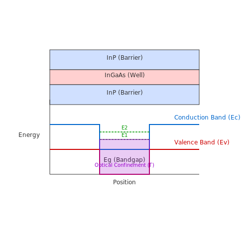
MBE-grown quantum well (QW) lasers exhibit superior performance due to the tight confinement of charge carriers within nanoscale active regions. The quantized energy levels in a QW structure enhance the density of states near the band edge, leading to lower threshold currents and higher differential gain. The modal gain g in a QW laser is given by:
where Γ is the optical confinement factor and gmaterial is the material gain. For an InGaAs/InP QW laser emitting at 1.55 µm, the confinement factor can be approximated as:
Here, neff is the effective refractive index, d is the well thickness, and λ is the emission wavelength. MBE allows d to be controlled with sub-nanometer precision, enabling tailored emission spectra.
High-Speed Photodetectors
MBE facilitates the growth of low-defect absorption layers and tailored bandgap materials for photodetectors. For instance, InGaAs-based photodiodes leverage MBE's ability to precisely adjust the In/Ga ratio to optimize responsivity in the near-infrared (NIR) range. The quantum efficiency η of a photodetector is governed by:
where R is the surface reflectance, α is the absorption coefficient, and d is the absorption layer thickness. MBE's monolayer-level thickness control minimizes dark current while maximizing η.
LEDs with Strain-Compensated Multiquantum Wells
In GaN-based LEDs, MBE enables strain management in multiquantum well (MQW) structures through careful balancing of compressive and tensile layers. The piezoelectric polarization field in GaN/AlGaN MQWs can be mitigated by introducing strain-compensating layers, enhancing radiative recombination. The internal quantum efficiency (IQE) is expressed as:
where τrad and τnr are radiative and non-radiative lifetimes, respectively. MBE's in situ monitoring capabilities ensure optimal growth conditions to maximize τrad.
Challenges and Innovations
Despite its advantages, MBE faces challenges in scaling for mass production due to low growth rates (<1 µm/hr) and high equipment costs. Recent advances include:
- Gas-source MBE (GSMBE): Combines MBE's precision with metalorganic precursors for higher throughput.
- Droplet-free growth: Techniques like migration-enhanced epitaxy (MEE) reduce oval defects in arsenide-based devices.
- Nitride MBE: Plasma-assisted MBE enables high-quality GaN layers for UV LEDs and power electronics.
These innovations expand MBE's role in next-generation optoelectronics, such as quantum dot lasers and topological insulator-based photonic devices.
4. Scalability and Throughput Issues
4.1 Scalability and Throughput Issues
Fundamental Limitations in MBE Growth Rates
The growth rate in MBE is fundamentally constrained by the flux of molecular or atomic beams impinging on the substrate. For a given material, the deposition rate R can be expressed as:
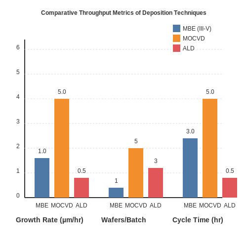
where J is the beam flux (atoms/cm²·s), A is the sticking coefficient, η is the incorporation efficiency, and n is the atomic density of the crystal (atoms/cm³). Typical growth rates for III-V compounds range from 0.1 to 1.0 μm/hr, significantly slower than chemical vapor deposition (CVD) techniques.
Chamber Size and Wafer Scaling Challenges
MBE systems face inherent scalability constraints due to:
- Beam uniformity requirements: Maintaining <1% thickness variation across 300mm wafers demands precise source-to-substrate distance optimization.
- Vacuum pumping limitations: Larger chambers require exponentially greater pumping capacity to maintain ultra-high vacuum (UHV) below 10⁻¹⁰ Torr.
- Source depletion effects: Effusion cell depletion rates increase nonlinearly with larger wafer areas, requiring frequent source replenishment.
Throughput Bottlenecks in Production Environments
The serial nature of MBE processing creates multiple throughput constraints:
Typical cycle times for 200mm wafers exceed 8 hours, with the growth phase accounting for only 30-50% of total process time. The UHV requirements necessitate lengthy pump-down and bake-out cycles between runs.
Comparative Throughput Metrics
| Process | Growth Rate (μm/hr) | Wafers/Batch | Cycle Time (hr) |
|---|---|---|---|
| MBE (III-V) | 0.1-1.0 | 1-3 | 6-12 |
| MOCVD | 2-10 | 5-25 | 2-4 |
| ALD | 0.01-0.1 | 25-50 | 1-3 |
Emerging Solutions for Scalability
Recent developments aim to address these limitations:
- Multi-wafer systems: Cluster tools with 3-5 growth chambers sharing a central transfer module can improve throughput by 2-3×.
- Gas-source MBE: Hybrid approaches using metalorganics for group III elements achieve higher growth rates while maintaining abrupt interfaces.
- Plasma-assisted doping: RF plasma sources enable faster doping profile control compared to thermal effusion cells.
Thermal Budget Considerations
The thermal cycle in MBE presents additional constraints:
where ρ is density, cp is heat capacity, V is wafer volume, and h is the heat transfer coefficient. The slow heating/cooling rates required to prevent thermal stress in compound semiconductors further limit throughput.
4.2 Integration with Other Fabrication Techniques
Hybrid Deposition Approaches
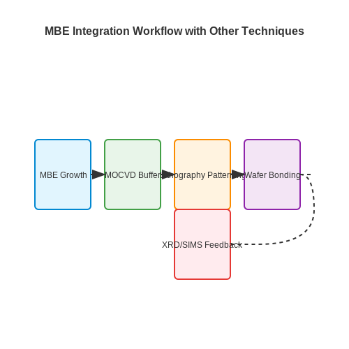
Molecular Beam Epitaxy (MBE) is often combined with Metal-Organic Chemical Vapor Deposition (MOCVD) to exploit the complementary strengths of each technique. MBE provides ultra-high-precision monolayer control, while MOCVD offers higher throughput and scalability for industrial applications. For instance, InGaAs-based high-electron-mobility transistors (HEMTs) frequently use MBE for the active quantum well layers and MOCVD for the buffer layers to minimize defects.
Lithographic Patterning Compatibility
MBE-grown heterostructures must interface seamlessly with electron-beam lithography (EBL) and photolithography. The ultra-clean MBE environment minimizes surface oxides, improving resist adhesion and pattern fidelity. However, post-growth processing requires careful thermal budget management to avoid interdiffusion at epitaxial interfaces. A common workflow involves:
- MBE growth of the heterostructure
- Low-temperature atomic layer deposition (ALD) of a protective capping layer
- Room-temperature lithographic patterning
- Dry etching using reactive ion etching (RIE) with chemistry tuned to the MBE material system
In-Situ Characterization Synergies
MBE chambers increasingly integrate in-situ characterization tools such as:
where τ represents the damping time constant of intensity oscillations during layer-by-layer growth. This real-time feedback enables immediate adjustments before subsequent processing steps.
Wafer Bonding for Heterogeneous Integration
Direct wafer bonding of MBE-grown III-V materials to silicon substrates enables photonic-electronic co-integration. The key challenges involve:
- Thermal expansion coefficient mismatch (Δα/α ~ 10-6 K-1 for GaAs/Si)
- Surface roughness requirements (< 0.5 nm RMS for successful bonding)
Advanced techniques like plasma-activated bonding achieve void-free interfaces with bond strengths exceeding 1 J/m2.
Metrology Feedback Loops
Post-growth characterization data from techniques such as:
- X-ray diffraction (XRD) for strain analysis
- Secondary ion mass spectrometry (SIMS) for dopant profiling
are increasingly fed back into MBE growth control systems using machine learning algorithms to optimize subsequent runs. This closed-loop approach reduces trial-and-error iterations by up to 40% in complex multilayer structures.
Selective Area Epitaxy Integration
MBE combined with dielectric-patterned substrates enables selective area growth for quantum dot arrays and nanowires. The growth rate differential between masked and unmasked regions follows:
where Jad and Jdes are the adsorption and desorption fluxes, and Ea is the activation energy for surface migration.
4.3 Emerging Materials for MBE
Topological Insulators
Molecular Beam Epitaxy (MBE) has enabled the growth of high-quality topological insulators (TIs) such as Bi2Se3, Bi2Te3, and Sb2Te3. These materials exhibit a bulk insulating state with conducting surface states protected by time-reversal symmetry. The key challenge in MBE growth is minimizing bulk conduction by controlling defects and doping. For instance, compensating intrinsic n-type defects in Bi2Se3 requires precise stoichiometry and substrate temperature tuning between 200–300°C.
where Eg is the effective gap, vF the Fermi velocity, a the lattice constant, and Δ the hybridization gap. MBE-grown TIs are critical for spintronics and quantum computing applications due to their robust spin-momentum locking.
Two-Dimensional Transition Metal Dichalcogenides
MBE growth of monolayer MoS2, WS2, and WSe2 has advanced through substrate engineering and flux ratio optimization. Unlike exfoliation, MBE enables wafer-scale growth with controlled defects. The critical parameters include:
- Substrate choice: Epitaxial alignment on sapphire (0001) or graphene.
- Chalcogen/metal flux ratio: Typically >20:1 to suppress metal clustering.
- Growth temperature: 400–700°C for optimal adatom mobility.
Recent work demonstrates room-temperature photoluminescence in MBE-grown MoSe2 with linewidths <50 meV, rivaling exfoliated flakes.
III-Nitride Heterostructures
Ultrawide-bandgap materials like β-Ga2O3 and AlN are gaining traction for high-power electronics. MBE growth of β-Ga2O3 requires oxygen-plasma-assisted techniques to achieve stoichiometric films. Key advances include:
- Delta-doping of Si in Ga2O3 with mobilities >100 cm2/V·s.
- AlN/GaN superlattices with threading dislocation densities <106 cm−2.
The breakdown field Ebr in these materials scales as:
Oxide Perovskites
MBE of complex oxides like SrTiO3 and LaAlO3 enables atomically sharp interfaces with emergent 2D electron gases (2DEGs). The growth window is narrow—typically 600–800°C under ozone or oxygen plasma. Stoichiometry is monitored via reflection high-energy electron diffraction (RHEED) oscillations. Recent breakthroughs include:
- Ferroelectric BaTiO3 integrated with Si using SrTiO3 buffer layers.
- Magnetic Weyl semimetals in NdNbO3/EuO heterostructures.
Dilute Nitrides and Bismides
MBE enables metastable alloys like GaAs1−xNx (x < 0.05) and GaAs1−yBiy (y < 0.1) for infrared optoelectronics. The large miscibility gaps require low growth temperatures (<400°C) and precise flux control. Bi incorporation follows:
where kB is a kinetic prefactor, Ea the incorporation barrier (~1.3 eV), and PBi2 the Bi2 beam equivalent pressure.
5. Key Research Papers
5.1 Key Research Papers
- CHAPTER 4 Molecular Beam Epitaxy (MBE - Academia.edu — GaAs IMPATT diodes prepared by molecular beam epitaxy. Appl Phys Lett 1974; 25: 224-226. Cho AY, Ballamy WC. GaAs planar technology by molecular beam epitaxy (MBE). J Appl Phys 1975; 46: 783-785. Cho AY, Reinhart FK. Growth of three-dimensional dielectric waveguides for integrated optics by molecular-beam-epitaxy method. Appl Phys Lett 1972; 21 ...
- Molecular-beam epitaxy - Wikipedia — A simple sketch showing the layout of the main chamber in a molecular-beam epitaxy system. Molecular-beam epitaxy (MBE) is an epitaxy method for thin-film deposition of single crystals.MBE is widely used in the manufacture of semiconductor devices, including transistors. [1] MBE is used to make diodes and MOSFETs (MOS field-effect transistors) at microwave frequencies, and to manufacture the ...
- III-V Semiconductor Materials Grown by Molecular Beam Epitaxy for ... — Molecular Beam Epitaxy technology can be used to precisely control the composition of such compounds to tailor electronic and optical properties with much more freedom than in the case of elemental semiconductors such as silicon. Molecular Beam Epitaxy [9] Molecular Beam Epitaxy (MBE) is a precisely controlled evaporation
- PDF Molecular Beam Epitaxy - Springer — Molecular Beam Epitaxy P.R Vaya and K. Ponnuraju Semiconductor Device Research Laboratory, Centre for Systems and Devices Indian Institute of Technology, Madras-600 036, India Molecular Beam Epitaxy (MBE) has become a well-established technique for the growth of ultra-thin films and devices with precise control
- PDF Silicon/Germanium Molecular Beam Epitaxy - DiVA — Molecular Beam Epitaxy Physics D-level Thesis Date/Term: 2006-04-25 Supervisor: Prof. Kjell Magnusson Examiner: Prof. Lars Johansson Serial Number: 2006-02 Karlstads universitet 651 88 Karlstad Tfn 054-700 10 00 Fax 054-700 14 60 [email protected] www.kau.se
- Basics of Molecular Beam Epitaxy (MBE) technique - ResearchGate — Molecular Beam Epitaxy (MBE) Silicon Based Thin Film Solar Cells 101 section 5.2 can be used to rep resent the relati ve atom positi ons in mat rix and twin. Fig. 21 shows the stacking sequence of ...
- Methods and optoelectronic device applications of semiconductor epitaxy ... — Here, non-destructive microstructural analysis of the initial stages of the semiconductor epitaxy using 2D materials, vertical integration of semiconductor devices using freestanding 2D substrates, and fabrication of detachable semiconductor devices using 2D-assisted lift-off are detailed.
- Molecular beam epitaxy of III-V semiconductors - Taylor & Francis Online — Molecular beam epitaxy (MBE) has been instrumental in the advancement of the physics and technology of semiconductors that has occurred over the last few decades. The III-V material system has led the way in these new developments.
- Principles of Molecular Beam Epitaxy - ScienceDirect — Molecular beam epitaxy (MBE) is an elegant material growth technique that is most simply described as a very refined form of vacuum evaporation or physical vapor deposition, with exquisite control over material purity, interface formation, alloy compositions, and doping concentrations. ... MBE has become not only a research growth technique ...
- PDF MOLECULAR BEAM EPITAXY: PRINCIPLES AND APPLICATIONS - ResearchGate — Molecular Beam Epitaxy (MBE) is an Ultra-High-Vacuum (UHV)-based technique for producing high quality epitaxial structures with monolayer (ML) control. Since its
5.2 Textbooks on MBE
- Molecular Beam Epitaxy - Wiley Online Library — 14. Molecular-Beam Epitaxy of Antimonides for Optoelectronic Devices 233 Eric Tournie 14.1 Introduction 233 14.2 EpitaxyofAntimonides:ABriefHistoricalSurvey 235 14.3 Molecular-BeamEpitaxyofAntimonide 236 14.3.1 SubstratePreparation 236 14.3.2 DopingofIII-SbCompounds 237 14.3.3 ControlofAlloyCompositions 239 14.3.4 No-Common-AtomInterfaces 241
- PDF Molecular Beam Epitaxy - external.dandelon.com — in MBE Systems 107 3.2.1 The Hot-Wall Beam Epitaxy Growth System 108 3.2.2 Focused Ion Beam Technology 113 Part III Characterization Methods 4. In-Growth Characterization Techniques 120 4.1 RHEED 121 4.1.1 Fundamentals of Electron Diffraction 122 4.1.2 Origin of RHEED Features 129 4.1.3 RHEED Data from Reconstructed Semiconductor Surfaces 134
- Udo W. Pohl. Epitaxy of Semiconductors-Physics and Fabrication of ... — basis for the fabrication of semiconductor heterostructures and devices. ... lh light hole LPE liquid phase epitaxy MBE molecular beam epitaxy ML monolayer MOCVD metal-organic chemical vapor deposition MOMBE metal-organic molecular beam ... and T is the absolute tem-perature in K. Values for some cubic semiconductors are given in Table 2.5. 2.1 ...
- Molecular beam epitaxy fabrication of two-dimensional materials — Among them, molecular beam epitaxy (MBE) has been proven to be outstanding in the synthesis of 2D materials. MBE is an epitaxial process, in which growth of the thin film takes place on a heated crystalline substrate through the interaction of adsorbed species supplied by atomic or molecular beams under ultrahigh vacuum (UHV) conditions [11 ...
- Molecular Beam Epitaxy: Materials and Applications for Electronics and ... — Covers both the fundamentals and the state-of-the-art technology used for MBE Written by expert researchers working on the frontlines of the field, this book covers fundamentals of Molecular Beam Epitaxy (MBE) technology and science, as well as state-of-the-art MBE technology for electronic and optoelectronic device applications. MBE applications to magnetic semiconductor materials are also ...
- Molecular Beam Epitaxy | Wiley Online Books — Covers both the fundamentals and the state-of-the-art technology used for MBE Written by expert researchers working on the frontlines of the field, this book covers fundamentals of Molecular Beam Epitaxy (MBE) technology and science, as well as state-of-the-art MBE technology for electronic and optoelectronic device applications. MBE applications to magnetic semiconductor materials are also ...
- CHAPTER 4 Molecular Beam Epitaxy (MBE - Academia.edu — Hull D, Bacon DJ. Introduction to dislocations. Oxford: Butterworth-Heinemann 2001. Chang LL, Ploog K. Molecular Beam Epitaxy and Heterostructures. NATO ASI Ser, Ser E 87, Dordrecht: Martinus Nijhoff 1985. Heckingbottom R, Todd CJ, Davies GJ. The Interplay of Thermodynamics and Kinetics in Molecular Beam Epitaxy (MBE) of Doped Gallium Arsenide.
- Basics of Molecular Beam Epitaxy (MBE) technique — Molecular Beam Epitaxy (MBE) Silicon Based Thin Film Solar Cells 85 R molecules s8.33 1022 pAe 1 MT (1) where p is the pressure in the effusion cell, Ae is the surface area from which molecules evaporate, M is the molecular weight of the evaporating species and T is the temperature of the melt. Combining the Knudsen equation with the cosine law (given that the ideal Knudsen cell exhibits
- Basics of Molecular Beam Epitaxy (MBE) technique - ResearchGate — Molecular Beam Epitaxy (MBE) Silicon Based Thin Film Solar Cells 101 section 5.2 can be used to rep resent the relati ve atom positi ons in mat rix and twin. Fig. 21 shows the stacking sequence of ...
- PDF Silicon/Germanium Molecular Beam Epitaxy - DiVA — 1.1 Molecular Beam Epitaxy The process MBE (Molecular Beam Epitaxy) studied in this master's thesis is roughly speaking a matter of growing a crystal on top of another. The word epitaxy describes that the atoms, or molecules, that hit the substrate order themselves according to the lattice structure of the substrate.
5.3 Online Resources and Tutorials
- PDF Understanding thin film formation through molecular beam epitaxy ... — Understanding thin film formation through Molecular Beam epitaxy studies of atomic-level interactions in order to link deposition process conditions to device performance in 2 materials: MgO and Cs3Sb A Dissertation Presented By Sue-Jonnathane Celestin to The Department of Chemical Engineering
- Towards "on-demand" van der Waals epitaxy with hpc-driven online ... — The global sampling opportunities boosted by extreme-scale resource-driven batch acquisition workflows and on-the-fly analysis and UQ capabilities are ideally suited to pin down more sophisticated interplay of thermodynamic and kinetic factor driving self-organized and strain-engineered interfacial evolution during vdW epitaxy.
- PDF Chapter 3. Molecular Beam Epitaxy of Compound Semiconductors — introduction and in-situ surface analysis and metalization. The multichamber epitaxy system allows for the fabrication of a large number of different heterostructures completely within a continuous ultrahigh vacuum environment. The interconnected reactors enable an additional degree of freedom in device design by providing the ability to integrate
- Molecular beam epitaxy : materials and applications for electronics and ... — Publisher's summary Covers both the fundamentals and the state-of-the-art technology used for MBE Written by expert researchers working on the frontlines of the field, this book covers fundamentals of Molecular Beam Epitaxy (MBE) technology and science, as well as state-of-the-art MBE technology for electronic and optoelectronic device ...
- (PDF) CHAPTER 4 Molecular Beam Epitaxy (MBE - Academia.edu — Molecular Beam Epitaxy (MBE) represents a widely used growth technique to approach the basic research applied to the growth of semiconductor films and multilayer structures. The main features that distinguish the MBE from other growth techniques are the precise reproducibility of all parameters involved during the epitaxial process, the growth conditions far from thermodynamic equilibrium, and ...
- PDF AN INTRODUCTION TO MOLECULAR BEAM EPITAXY - Springer — l electronic and optoelec tronic devices. These include in-situ growth of two-dimensional patterns by Si02 masking[l] or shadow masking[41] of the substrate. epitaxial overgrowth on top of etched or partially processed structures. pseudornorphic growth of strained layers[42] of materials with different lattice constants. and beteroepjtaxy ...
- Basics of Molecular Beam Epitaxy (MBE) technique — Abstract: Molecular Beam Epitaxy (MBE) represents a widely used growth technique to approach the basic research applied to the growth of semiconductor films and multilayer structures. The main features that distinguish the MBE from other growth techniques are the precise reproducibility of all parameters involved during the epitaxial process, the growth conditions far from thermodynamic ...
- PDF Molecular beam epitaxy : materials and applications for electronics and ... — 5. Ammonia Molecular Beam Epitaxy of Ill-Nitrides Micha N. Fireman and James S. Speck
- Basics of Molecular Beam Epitaxy (MBE) technique — Molecular Beam Epitaxy (MBE) represents a widely used growth technique to approach the basic research applied to the growth of semiconductor films and multilayer structures. The main features that ...
- Molecular Beam Epitaxy : Fundamentals and Current Status — This book, which presents a review of the state of the art of molecular beam epitaxy (MBE), as applied to the growth of semiconductor films and multilayer structures, may serve the reader as a convenient general guide to the topics related to this crystallization technique.