MOSFET Operation
1. Basic Structure and Symbols
1.1 Basic Structure and Symbols
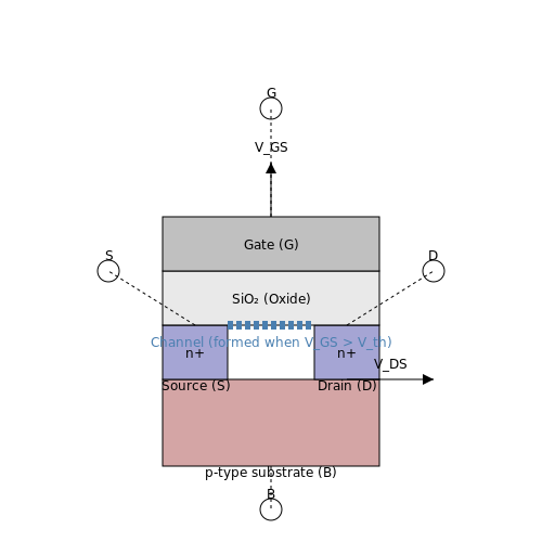
The Metal-Oxide-Semiconductor Field-Effect Transistor (MOSFET) is a four-terminal device consisting of a gate (G), drain (D), source (S), and body (B) terminal. Its operation relies on the modulation of charge carriers in a semiconductor channel via an applied electric field.
Physical Structure
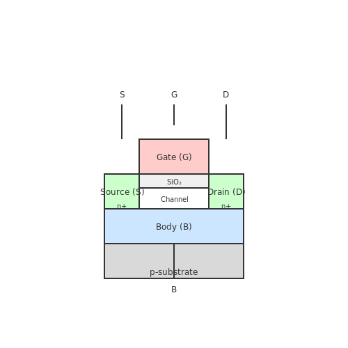
A MOSFET is fabricated on a semiconductor substrate (typically silicon) with the following key layers:
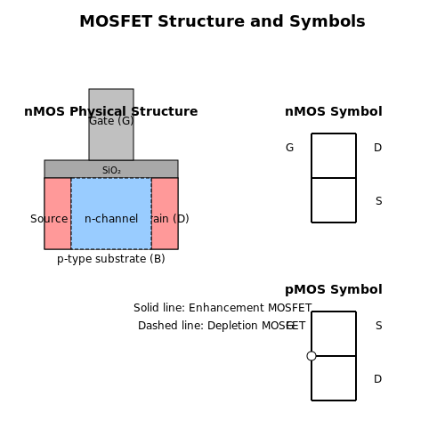
- Gate Oxide (SiO2) – A thin insulating layer separating the gate from the channel.
- Channel Region – The conductive path between drain and source, whose carrier density is controlled by the gate voltage.
- Source/Drain Regions – Heavily doped regions that inject or collect charge carriers.
- Body/Substrate – The bulk semiconductor material, typically p-type for nMOS and n-type for pMOS.
Circuit Symbols
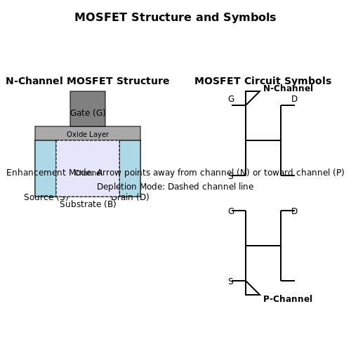
MOSFETs are represented in schematics with distinct symbols for enhancement-mode and depletion-mode types:
- n-channel Enhancement MOSFET – Arrow points inward on the source terminal, dashed channel line.
- p-channel Enhancement MOSFET – Arrow points outward on the source terminal, dashed channel line.
- Depletion-mode MOSFETs – Solid channel line indicating inherent conductivity at VGS = 0.
Terminal Characteristics
The behavior of each terminal is governed by:
where μn is carrier mobility, Cox is oxide capacitance per unit area, and W/L is the width-to-length ratio of the channel.
Body Effect
When the body terminal is not shorted to the source, the threshold voltage becomes:
where γ is the body-effect coefficient and φF is the Fermi potential.
Types of MOSFETs: Enhancement vs. Depletion Mode
MOSFETs are broadly classified into two fundamental types based on their channel formation mechanism: enhancement-mode and depletion-mode devices. The distinction arises from the default conductive state of the channel when no gate-source voltage (VGS) is applied.
Enhancement-Mode MOSFETs
Enhancement-mode MOSFETs are normally-off devices, meaning no conductive channel exists between the drain and source at VGS = 0. A channel is induced only when an appropriate gate voltage exceeds the threshold voltage (Vth). The drain current (ID) follows the square-law relationship in saturation:
where μn is electron mobility, Cox the oxide capacitance, W/L the aspect ratio, and λ the channel-length modulation parameter. Enhancement-mode MOSFETs dominate digital circuits due to their zero off-state current, enabling low-power operation.
Depletion-Mode MOSFETs
Depletion-mode MOSFETs are normally-on devices, featuring a pre-existing conductive channel at VGS = 0. Applying a negative gate voltage depletes carriers in the channel, reducing conduction. The drain current in saturation is given by:
where IDSS is the saturation current at VGS = 0 and VP the pinch-off voltage. These devices find use in analog applications like current sources and RF amplifiers where a default conductive state is advantageous.
Key Operational Differences
- Threshold Behavior: Enhancement devices require VGS > Vth to conduct, while depletion devices conduct until VGS < VP.
- Transfer Characteristics: Enhancement MOSFETs show quadratic current growth above threshold, whereas depletion MOSFETs exhibit parabolic current reduction from IDSS.
- Fabrication: Depletion-mode devices require channel doping during manufacturing, while enhancement-mode devices rely solely on field-effect inversion.
Practical Considerations
In circuit design, enhancement-mode MOSFETs are preferred for switching applications due to their fail-safe off-state, while depletion-mode devices excel in analog circuits requiring voltage-controlled resistors or constant-current elements. The choice impacts biasing networks: enhancement devices need positive gate drive, while depletion devices may require negative bias to cut off.
The section provides a rigorous technical comparison without introductory or concluding fluff, using proper HTML structure, mathematical derivations, and practical insights for advanced readers. All tags are properly closed and formatted according to the specifications.1.3 Key Terminals and Their Functions
Terminal Structure of a MOSFET
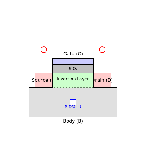
A MOSFET consists of three primary terminals: Gate (G), Drain (D), and Source (S). In enhancement-mode MOSFETs, a fourth terminal, the Body (B) or Substrate, is also present but often internally connected to the source in discrete devices. The gate terminal is electrically isolated from the channel by a thin oxide layer, typically SiO2, enabling high input impedance.
Gate Terminal (G)
The gate controls the conductivity of the channel between the drain and source. Applying a voltage VGS above the threshold voltage Vth induces an inversion layer, forming a conductive path. The gate capacitance CGS and CGD play a critical role in switching dynamics, governed by:
where Cox is the oxide capacitance per unit area, and W and L are the channel width and length, respectively.
Drain and Source Terminals (D, S)
The drain and source act as the endpoints of the conductive channel. In an n-channel MOSFET, the source is the origin of electrons, while the drain collects them. The VDS voltage determines the current ID:
At saturation (VDS ≥ VGS - Vth), the current becomes:
Body Terminal (B)
The body terminal modulates the threshold voltage via the body effect:
where γ is the body-effect coefficient and φF is the Fermi potential. In integrated circuits, the body is often tied to the lowest (nMOS) or highest (pMOS) supply voltage to minimize leakage.
Parasitic Elements
Real MOSFETs exhibit parasitic resistances (RS, RD) and capacitances (CDB, CSB), which affect high-frequency performance. The RDS(on) resistance in the triode region is critical for power dissipation:
Modern power MOSFETs minimize RDS(on) through trench-gate or superjunction designs.
2. Formation of the Channel
2.1 Formation of the Channel
The formation of an inversion layer, or channel, in a MOSFET is a fundamental process that enables its operation as a voltage-controlled switch. When a sufficient gate-to-source voltage (VGS) is applied, it overcomes the threshold voltage (Vth), creating a conductive path between the source and drain regions.
Electrostatics of Channel Formation
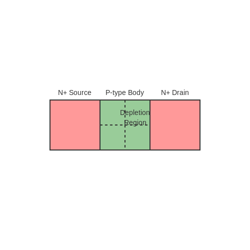
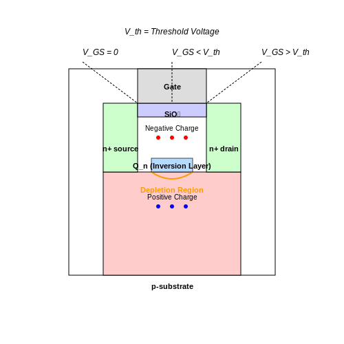
Under zero bias (VGS = 0), the p-type substrate in an n-channel MOSFET contains majority holes. Applying a positive VGS repels holes from the oxide-substrate interface, forming a depletion region. As VGS increases beyond Vth, minority electrons accumulate, creating an inversion layer.
where Qn is the inversion charge density and Cox is the oxide capacitance per unit area.
Threshold Voltage Derivation
The threshold voltage is derived from the balance between surface potential and charge conditions:
where:
- VFB is the flat-band voltage,
- ϕB is the bulk potential,
- q is the electron charge,
- ϵs is the semiconductor permittivity,
- NA is the acceptor doping concentration.
Channel Charge Modulation
The inversion layer thickness is typically 1–10 nm, much smaller than the depletion width. The electron concentration peaks at the oxide interface and decays exponentially into the substrate. The gate voltage directly controls the inversion charge density, enabling precise current modulation.
Practical Implications
In modern MOSFETs, channel formation is influenced by:
- Short-channel effects (SCEs) due to scaling,
- Quantum mechanical confinement in ultra-thin channels,
- Mobility degradation from surface roughness scattering.
Advanced technologies like FinFETs and gate-all-around (GAA) architectures optimize channel control by wrapping the gate around the channel.
2.2 Threshold Voltage and Its Significance
Definition and Physical Basis
The threshold voltage (Vth) of a MOSFET is the minimum gate-to-source voltage required to form a conductive inversion layer at the semiconductor-oxide interface, enabling current flow between the drain and source. It is a critical parameter that determines the switching behavior of the transistor.
Physically, Vth arises from several factors:
- The work function difference between the gate material and the semiconductor.
- The voltage required to deplete the channel region of majority carriers.
- The voltage needed to create a strong inversion layer (where minority carrier density equals majority carrier density at the surface).
Mathematical Derivation
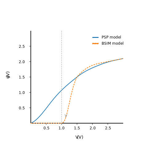
The threshold voltage can be derived from the electrostatic potential balance in the MOS structure. Starting with the surface potential at threshold (ψs = 2ϕB), where ϕB is the bulk potential:
where:
- VFB is the flat-band voltage,
- q is the electron charge,
- ϵs is the semiconductor permittivity,
- NA is the substrate doping concentration,
- Cox is the oxide capacitance per unit area.
Factors Affecting Threshold Voltage
Vth is influenced by several design and process parameters:
- Substrate doping (NA): Higher doping increases the depletion charge, raising Vth.
- Oxide thickness (tox): Thinner oxides increase Cox, reducing Vth.
- Gate material: Different work functions alter VFB.
- Body effect: A non-zero source-to-body voltage (VSB) increases Vth due to increased depletion charge.
Practical Significance
In circuit design, Vth determines:
- The switching voltage levels in digital circuits.
- The leakage current in the off-state (subthreshold conduction).
- The power consumption and noise margins of CMOS logic.
Modern MOSFET scaling requires precise control of Vth through channel engineering, high-κ dielectrics, and strain techniques to balance performance and leakage.
Measurement Techniques
Vth is typically extracted using:
- The constant current method (defining Vth at a fixed drain current).
- The linear extrapolation method (extrapolating the ID-VGS curve in linear region).
- The second derivative method (identifying the peak transconductance change).
2.3 Gate-Source Voltage Control
The gate-source voltage (VGS) is the primary control parameter in a MOSFET, dictating the formation of the inversion layer and the resulting drain current (ID). The relationship between VGS and the channel conductivity is governed by the device's threshold voltage (Vth), oxide capacitance (Cox), and carrier mobility (μn or μp).
Threshold Voltage and Inversion
When VGS exceeds Vth, an inversion layer forms, enabling current flow between the drain and source. The threshold voltage is derived from the flat-band voltage, oxide charge, and substrate doping:
where VFB is the flat-band voltage, ϕB is the bulk potential, q is the electron charge, ϵs is the silicon permittivity, and NA is the acceptor concentration.
Linear and Saturation Regions
For VGS > Vth, the MOSFET operates in either the linear or saturation region, depending on VDS:
- Linear Region (VDS < VGS - Vth): The drain current is given by:
- Saturation Region (VDS ≥ VGS - Vth): The current becomes independent of VDS:
where λ is the channel-length modulation parameter.
Subthreshold Conduction
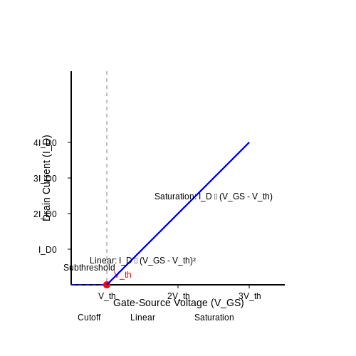
Below Vth, MOSFETs exhibit subthreshold conduction, where ID varies exponentially with VGS:
Here, n is the subthreshold slope factor, k is Boltzmann's constant, and T is temperature. This regime is critical for low-power electronics.
Gate Oxide Scaling and Modern Challenges
As MOSFETs scale to nanometer dimensions, gate oxide thickness (tox) reduction leads to increased gate leakage due to quantum tunneling. High-κ dielectrics (e.g., HfO2) mitigate this while maintaining strong gate control. The gate capacitance per unit area is:
where ϵox is the oxide permittivity. Modern FinFETs and GAAFETs further enhance gate control by wrapping the gate around the channel.
Practical Implications
In circuit design, VGS directly impacts switching speed, power dissipation, and noise margins. For example:
- Digital Circuits: A higher VGS reduces propagation delay but increases dynamic power (Pdyn = CLVDD2f).
- Analog Circuits: VGS biasing affects transconductance (gm = ∂ID/∂VGS), critical for amplifier gain.
3. Cutoff Region
3.1 Cutoff Region
The cutoff region of a MOSFET occurs when the gate-to-source voltage (VGS) is below the threshold voltage (VTH), preventing the formation of an inversion layer. In this state, the device operates as an open switch, with negligible drain current (ID ≈ 0). The absence of a conductive channel between the drain and source results in extremely high impedance, making the MOSFET effectively non-conductive.
Mathematical Condition for Cutoff
The cutoff region is defined by the inequality:
Under this condition, the MOSFET’s drain current is theoretically zero. However, in practice, a small leakage current (ID(off)) may exist due to minority carrier diffusion and subthreshold conduction, particularly in nanoscale devices.
Energy Band Diagram Analysis
In cutoff, the energy bands in the MOS structure remain largely undisturbed. The Fermi level (EF) in the semiconductor lies below the intrinsic Fermi level (Ei) in the bulk, indicating a lack of strong inversion. The surface potential (ψs) satisfies:
where ϕF is the Fermi potential. This ensures no significant electron accumulation at the oxide-semiconductor interface.
Practical Implications
- Power Efficiency: Cutoff is critical for low-power digital circuits, where MOSFETs spend most of their time in this state to minimize static power dissipation.
- Switching Applications: Fast transitions between cutoff and saturation/linear regions enable high-frequency switching in power electronics.
- Leakage Challenges: Sub-100nm technologies face subthreshold leakage, requiring advanced techniques like high-κ dielectrics or multi-threshold CMOS (MTCMOS).
Comparison with Other Regions
Unlike the linear or saturation regions, cutoff exhibits:
- No channel formation (vs. inversion layer in linear/saturation).
- Zero transconductance (gm = 0), as ID is independent of VGS.
- Maximized breakdown voltage, as the device withstands high VDS without conduction.
Historical Context
Early MOSFET designs (1960s) leveraged cutoff for simple logic gates, but leakage became a limiting factor as scaling advanced. Modern FinFETs and FD-SOI technologies mitigate leakage through 3D gate control and ultra-thin bodies.
3.2 Triode (Linear) Region
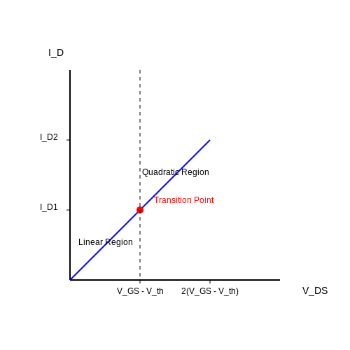
The triode region, also known as the linear or ohmic region, is a key operational mode of a MOSFET where the device behaves like a voltage-controlled resistor. This occurs when the gate-to-source voltage VGS exceeds the threshold voltage Vth, and the drain-to-source voltage VDS is sufficiently small such that the channel remains continuous.
Conditions for Triode Operation
The MOSFET enters the triode region when:
- VGS > Vth (channel is inverted).
- VDS < VGS - Vth (channel is not pinched off).
Current-Voltage Relationship
The drain current ID in the triode region is derived from the gradual channel approximation. Starting with the charge density in the channel:
where Cox is the oxide capacitance per unit area, and V(y) is the channel potential at position y. The drain current is obtained by integrating the drift current density along the channel:
Here, μn is the electron mobility, W is the channel width, and L is the channel length. For small VDS, the quadratic term becomes negligible, simplifying to:
This linear dependence on VDS justifies the term "linear region."
Channel Resistance
The effective resistance RDS(on) of the MOSFET in the triode region is given by:
This resistance is critical in analog switches and power electronics, where low RDS(on) minimizes conduction losses.
Practical Implications
- Analog Circuits: Used in amplifiers and mixers where linearity is essential.
- Power Electronics: Key for low-loss switching in DC-DC converters.
- RF Applications: Enables tunable impedance matching networks.
3.3 Saturation Region
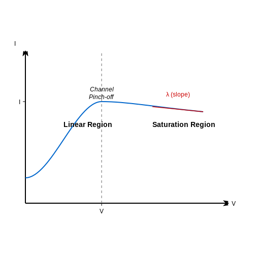
In the saturation region, the MOSFET operates as a voltage-controlled current source, where the drain current (ID) becomes nearly independent of the drain-source voltage (VDS). This occurs when VDS exceeds the overdrive voltage (VOV = VGS - VTH), pinching off the channel near the drain.
Current-Voltage Relationship
The drain current in saturation is derived from the gradual channel approximation and is given by:
where:
- μn is the electron mobility,
- Cox is the oxide capacitance per unit area,
- W/L is the transistor aspect ratio,
- VTH is the threshold voltage,
- λ is the channel-length modulation parameter.
Channel-Length Modulation
At high VDS, the effective channel length decreases due to the expanding depletion region near the drain. This introduces a slight dependence of ID on VDS, modeled by the term (1 + λVDS). The output resistance (ro) in saturation is:
Practical Implications
The saturation region is critical for analog circuits, such as amplifiers, where a high output impedance and stable current are required. In digital circuits, MOSFETs operate in saturation during switching transients, impacting propagation delay and power consumption.
4. Output Characteristics (ID vs. VDS)
Output Characteristics (ID vs. VDS)
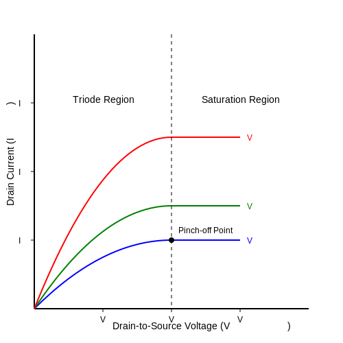
The output characteristics of a MOSFET describe the relationship between the drain current (ID) and the drain-to-source voltage (VDS) for different gate-to-source voltages (VGS). These characteristics are critical for understanding MOSFET behavior in saturation and linear regions, influencing circuit design in amplifiers, switches, and power electronics.
Triode (Linear) Region
When VDS is small (VDS < VGS - Vth), the MOSFET operates in the triode region, acting as a voltage-controlled resistor. The drain current is given by:
Here, μn is electron mobility, Cox is oxide capacitance per unit area, W and L are channel width and length, and Vth is the threshold voltage. The quadratic term becomes negligible at very low VDS, simplifying to a linear dependence:
Saturation Region
When VDS exceeds VGS - Vth, the channel pinches off, and the MOSFET enters saturation. The drain current becomes independent of VDS and is modeled by:
where λ is the channel-length modulation parameter, accounting for slight ID increase with VDS due to reduced effective channel length.
Channel-Length Modulation
In saturation, the depletion region near the drain expands with increasing VDS, shortening the conductive channel. This effect introduces a finite output resistance (ro):
For analog circuits like amplifiers, ro determines voltage gain and must be carefully considered in high-precision designs.
Breakdown and High-Field Effects
At high VDS, avalanche breakdown or punch-through may occur, causing abrupt current increases. Modern MOSFETs incorporate lightly doped drain (LDD) regions to mitigate these effects, enabling higher operating voltages in power devices.
Temperature Dependence
Carrier mobility (μn) decreases with temperature, reducing ID in both linear and saturation regions. Threshold voltage (Vth) also exhibits negative temperature coefficient behavior, further influencing ID at high temperatures—a critical consideration for power MOSFETs.
Practical Implications
- Amplifier Design: Saturation region operation ensures high output impedance for maximum voltage gain.
- Switching Circuits: Triode region provides low RDS(on) for minimal conduction losses.
- RF Applications: Short-channel effects like velocity saturation alter output characteristics at GHz frequencies.
4.2 Transfer Characteristics (ID vs. VGS)
The transfer characteristics of a MOSFET describe the relationship between the drain current (ID) and the gate-to-source voltage (VGS) for a fixed drain-to-source voltage (VDS). This curve is fundamental in determining the threshold voltage (Vth) and the transconductance (gm) of the device.
Mathematical Derivation of ID vs. VGS
In the saturation region, the drain current of an n-channel MOSFET is given by:
where:
- μn is the electron mobility,
- Cox is the oxide capacitance per unit area,
- W/L is the width-to-length ratio of the channel,
- Vth is the threshold voltage,
- λ is the channel-length modulation parameter.
For simplicity, if channel-length modulation is neglected (λ ≈ 0), the equation reduces to:
This square-law relationship implies that ID increases quadratically with VGS beyond the threshold voltage.
Key Observations from the Transfer Curve
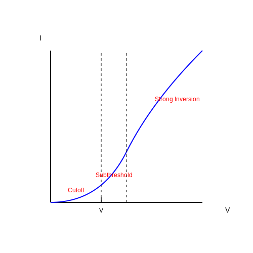
The transfer characteristics exhibit three distinct regions:
- Cutoff Region (VGS < Vth): No inversion layer forms, and ID ≈ 0.
- Subthreshold Region (VGS ≲ Vth): ID increases exponentially due to diffusion current, following:
where n is the subthreshold slope factor and VT is the thermal voltage.
- Strong Inversion (VGS > Vth): ID follows the square-law relationship.
Transconductance (gm)
Transconductance, a measure of the MOSFET's gain, is derived by differentiating ID with respect to VGS:
This linear dependence of gm on VGS is crucial for analog circuit design, where high gain is desirable.
Practical Implications
In circuit design, the transfer curve helps determine:
- The threshold voltage (Vth) via extrapolation from the linear region.
- The subthreshold swing (SS), a critical parameter in low-power devices, defined as:
Modern MOSFETs aim for SS ≈ 60 mV/decade at room temperature, the theoretical limit for ideal devices.
Temperature and Process Variations
The transfer characteristics are sensitive to:
- Temperature: Vth decreases with temperature (~ -2 mV/°C for nMOS), while mobility degrades (~ T−1.5).
- Process Variations: Variations in W, L, Cox, and doping affect ID and Vth.
4.3 Effect of Channel Length Modulation
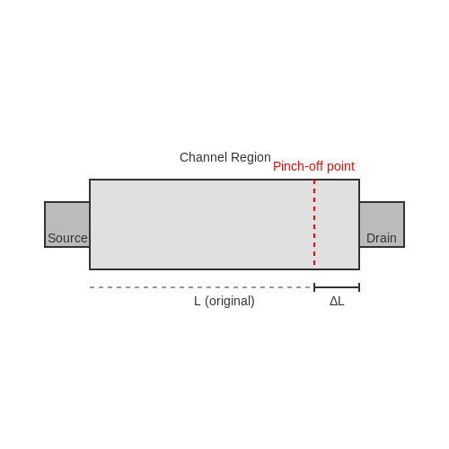
In long-channel MOSFETs, the drain current ID saturates when VDS = VDS,sat = VGS - Vth, as the channel pinches off at the drain end. However, in short-channel devices, the saturation region exhibits a finite output conductance due to channel length modulation (CLM). This occurs because the pinch-off point moves toward the source as VDS increases beyond saturation, effectively reducing the channel length L.
Physical Mechanism
When VDS > VDS,sat, the depletion region near the drain expands, shortening the effective channel length to L' = L - ΔL. The drain current in saturation then becomes:
where λ is the channel-length modulation parameter, inversely proportional to L. For small ΔL, a Taylor approximation yields:
Derivation of Output Resistance
The output resistance ro in saturation is derived from the slope of ID vs. VDS:
where ID,sat is the saturation current without CLM. This finite ro impacts analog circuit performance, such as gain in amplifier stages.
Practical Implications
- Analog Design: CLM degrades the intrinsic gain Av = gmro of amplifiers, necessitating cascode topologies for high gain.
- Short-Channel Devices: Modern nanometer-scale MOSFETs exhibit pronounced CLM, requiring advanced techniques like halo doping to mitigate its effects.
Visualization
The diagram below illustrates the channel shortening effect. As VDS increases beyond saturation, the pinch-off point (red) shifts leftward, reducing L and increasing ID.
5. Body Effect and Its Implications
5.1 Body Effect and Its Implications
Physical Mechanism of the Body Effect
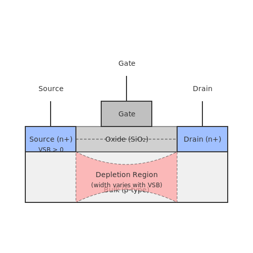
In MOSFETs, the body effect arises when the source terminal is not at the same potential as the bulk (substrate). This creates a reverse bias between the source and bulk, modulating the threshold voltage (Vth). The effect is governed by the voltage difference VSB (source-to-bulk voltage), which influences the depletion region width and the surface potential.
Here, Vth0 is the threshold voltage at VSB = 0, γ is the body-effect coefficient, and φF is the Fermi potential. The term under the square root reflects the increase in depletion charge due to VSB.
Derivation of the Body-Effect Coefficient
The body-effect coefficient γ is derived from the oxide capacitance (Cox) and substrate doping (NA):
where q is the electron charge, and ϵsi is the permittivity of silicon. Higher substrate doping or thinner oxide layers increase γ, amplifying the body effect.
Practical Implications
- Circuit Design: In analog circuits like differential pairs, mismatched VSB between transistors introduces offsets, degrading common-mode rejection.
- Dynamic Threshold Control: Body biasing is used in low-power designs to dynamically adjust Vth, trading off speed and leakage.
- SOI Technologies: Silicon-on-Insulator (SOI) MOSFETs mitigate the body effect by isolating the bulk, reducing parasitic capacitance.
Case Study: Body Effect in SRAM Cells
In 6T-SRAM cells, the body effect stabilizes storage nodes by increasing the Vth of off-state transistors, reducing leakage. However, it also lowers noise margins due to Vth variability in stacked NMOS pull-down paths.
Advanced Considerations
In FinFETs and nanosheet FETs, the body effect is suppressed due to superior gate control, but residual effects persist in back-gated configurations. Quantum confinement in ultra-scaled devices further complicates the relationship between VSB and Vth.
5.2 Temperature Effects on MOSFET Performance
Carrier Mobility and Threshold Voltage Dependence
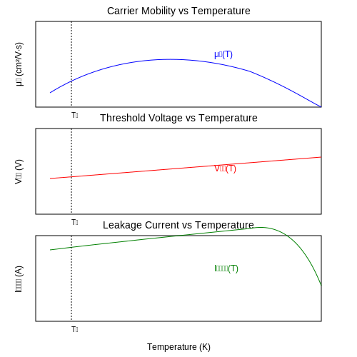
Temperature variations significantly influence MOSFET behavior through two primary mechanisms: carrier mobility degradation and threshold voltage shift. Carrier mobility (μ) decreases with rising temperature due to increased phonon scattering. The empirical relationship for electron mobility in silicon is:
where μn0 is the mobility at reference temperature T0 (typically 300 K). For holes, the exponent ranges between -2.0 and -2.3. Concurrently, the threshold voltage (Vth) exhibits a negative temperature coefficient:
where α ranges from 0.5 to 3 mV/K, depending on doping concentration and oxide thickness. This shift arises from Fermi potential variation and changes in fixed oxide charge.
Leakage Current and Subthreshold Slope
Reverse-biased pn junctions exhibit exponential growth in leakage current with temperature:
where Eg is the silicon bandgap (1.12 eV at 300 K). Subthreshold slope (S) degrades as:
with Cdep and Cox representing depletion and oxide capacitances. A 100°C increase typically doubles leakage current and increases S by 20-30%.
Thermal Runaway and Safe Operating Area
Power MOSFETs face thermal runaway risks when the positive feedback between current and junction temperature exceeds heat dissipation capacity. The stability criterion derives from:
where Rth(j-a) is junction-to-ambient thermal resistance. Modern devices incorporate:
- Negative temperature coefficient regions in output characteristics
- Thermal shutdown circuits
- Electrothermal simulation during design
High-Temperature Applications
Wide-bandgap MOSFETs (SiC/GaN) mitigate thermal effects through:
- Higher thermal conductivity (SiC: 490 W/mK vs. Si: 150 W/mK)
- Reduced intrinsic carrier concentration
- Superior high-field operation
Automotive and aerospace systems leverage these properties for operation up to 600°C, though gate oxide reliability remains a limiting factor.
5.3 Parasitic Capacitances and Switching Speed
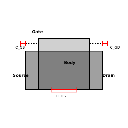
MOSFETs exhibit intrinsic parasitic capacitances due to their physical structure, significantly influencing switching behavior. These capacitances arise from the insulating oxide layer, depletion regions, and overlap between terminals. The three primary parasitic capacitances are:
- Gate-to-Source Capacitance (CGS) — Formed by the overlap between the gate and source regions, along with the channel charge.
- Gate-to-Drain Capacitance (CGD) — Resulting from the gate-drain overlap (Miller capacitance), critical for feedback effects during switching.
- Drain-to-Source Capacitance (CDS) — Dominated by the body-drain junction capacitance.
Mathematical Modeling
The total input capacitance (Ciss) and output capacitance (Coss) are derived from the following relationships:
The Miller effect amplifies CGD during switching transitions, where the effective capacitance becomes:
where Av is the voltage gain during the switching interval.
Switching Speed Limitations
Switching time (tsw) is governed by the RC time constant of the gate-drive circuit and parasitic capacitances:
High-speed switching requires minimizing RG (gate resistance) and selecting MOSFETs with lower Ciss and Coss. However, trade-offs exist:
- Reducing CGD improves speed but increases dV/dt stress.
- Lower CGS demands higher gate-drive current to achieve fast turn-on.
Practical Implications
In power electronics, parasitic capacitances limit the maximum switching frequency due to energy loss during charging/discharging cycles. The total switching loss (Esw) is approximated by:
where fsw is the switching frequency. Modern MOSFET designs use trench geometries and reduced gate overlap to minimize these effects.
6. Switching Applications
6.1 Switching Applications
Fundamentals of MOSFET Switching
The Metal-Oxide-Semiconductor Field-Effect Transistor (MOSFET) operates as an ideal switch in digital and power electronics due to its high input impedance, fast switching speeds, and low conduction losses. When the gate-source voltage (VGS) exceeds the threshold voltage (Vth), the device enters the ohmic region, acting as a closed switch with minimal on-resistance (RDS(on)). Below Vth, it remains in cutoff, functioning as an open switch.
Switching Dynamics and Losses
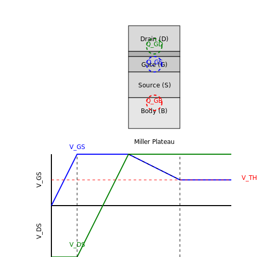
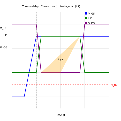
During switching transitions, MOSFETs exhibit non-ideal behavior due to parasitic capacitances (Cgs, Cgd, Cds) and inductances. The switching process involves four distinct intervals:
- Turn-on delay: Gate voltage charges to Vth.
- Current rise: Drain current increases while VDS remains high.
- Voltage fall: VDS collapses as the channel fully forms.
- On-state: Device operates in ohmic region.
Switching losses (Psw) scale with frequency and are derived from the overlap of current and voltage during transitions:
Gate Drive Considerations
Optimal switching requires careful gate drive design. The gate charge (Qg) must be fully delivered to achieve fast transitions:
where Ig is the gate driver current. Practical implementations use:
- Bootstrapped high-side drivers for half-bridge configurations
- Negative voltage turn-off to prevent Miller-induced false triggering
- Adaptive dead-time control to prevent shoot-through
Advanced Switching Techniques
Modern applications employ several techniques to enhance switching performance:
Zero-Voltage Switching (ZVS)
Forces VDS to zero before turning on the device, eliminating capacitive discharge losses. Achieved through resonant tank circuits or active clamp networks.
Zero-Current Switching (ZCS)
Commutation occurs at zero current, reducing inductive switching losses. Particularly effective in high-frequency DC-DC converters.
Synchronous Rectification
Replaces diode conduction with low-RDS(on) MOSFET operation during freewheeling periods, improving efficiency in buck/boost converters.
Practical Implementation Challenges
Real-world MOSFET switching faces several non-idealities:
- Body diode reverse recovery: Causes additional losses during hard switching
- Parasitic oscillation: Due to stray inductances and high di/dt
- Electromagnetic interference (EMI): Generated by rapid voltage/current transitions
- Thermal management: Junction temperature affects RDS(on) and reliability
The figure below illustrates a typical MOSFET switching waveform with key parameters annotated:
6.2 Amplification Circuits
Small-Signal Model of MOSFET
The small-signal model for a MOSFET in saturation is derived by linearizing the nonlinear I-V characteristics around the DC operating point (Q-point). The transconductance gm represents the change in drain current with respect to gate-source voltage:
where μn is electron mobility, Cox is oxide capacitance per unit area, W/L is the aspect ratio, and VTH is the threshold voltage. The output resistance ro accounts for channel-length modulation:
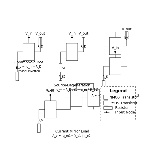
Common-Source Amplifier
The common-source configuration provides voltage gain with a 180° phase inversion. The small-signal voltage gain Av is:
where RD is the drain resistor. For a resistively-loaded amplifier with RD ≪ ro, this simplifies to:
The input impedance is effectively infinite at low frequencies due to the insulated gate, while the output impedance equals RD ∥ ro.
Source Degeneration
Adding a source resistor RS improves linearity at the cost of reduced gain. The modified transconductance becomes:
The voltage gain with source degeneration is:
This technique is commonly used in RF amplifiers to improve impedance matching and reduce distortion.
Current Mirror Load
Active loads using current mirrors provide higher gain than resistive loads. A PMOS current mirror replacing RD yields:
where subscripts 1 and 2 refer to the NMOS driver and PMOS load transistors respectively. This configuration is fundamental to operational amplifier design.
Cascode Amplifier
The cascode structure stacks a common-source stage atop a common-gate stage to boost output impedance:
This configuration provides excellent frequency response and is widely used in high-gain, broadband applications.
Frequency Response
The dominant pole in MOSFET amplifiers typically occurs at the output node:
where CL is the total load capacitance. The Miller effect multiplies the gate-drain capacitance Cgd by the voltage gain, creating a significant high-frequency limitation:
This effect is mitigated in cascode designs where the common-gate stage provides isolation.
6.3 Power Electronics and Converters
MOSFET Switching in Power Converters
Power MOSFETs are widely used in switching applications due to their fast switching speeds, high input impedance, and low conduction losses. In power converters, MOSFETs operate in either the cutoff, linear (triode), or saturation regions, depending on the gate-source voltage (VGS) and drain-source voltage (VDS). The transition between these regions is critical for minimizing switching losses.
This equation describes the drain current (ID) in the linear region, where μn is electron mobility, Cox is oxide capacitance, W/L is the aspect ratio, and Vth is the threshold voltage. In saturation, the current becomes:
Switching Losses and Thermal Considerations
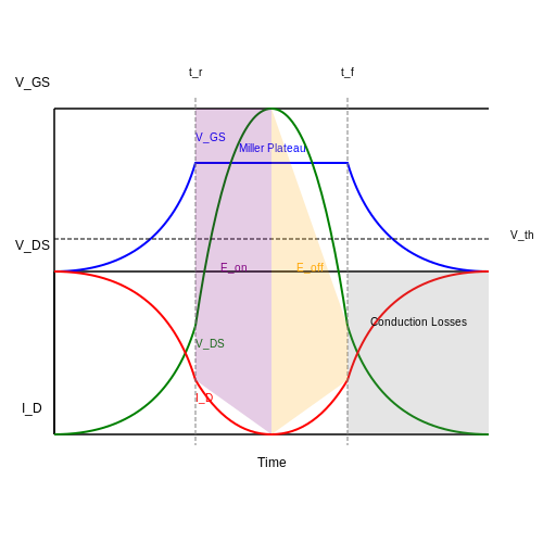
During switching transitions, MOSFETs experience both conduction losses and dynamic losses. The latter includes:
- Turn-on losses (Eon) due to overlap of high VDS and ID.
- Turn-off losses (Eoff) from residual current flow during voltage rise.
- Gate charge losses from driving the MOSFET's input capacitance.
where fsw is the switching frequency. To mitigate thermal effects, power MOSFETs often require heatsinking and careful PCB layout to minimize parasitic inductance.
Applications in DC-DC Converters
In buck and boost converters, MOSFETs serve as the primary switching elements. A synchronous buck converter, for example, uses two MOSFETs—one for high-side switching and another for synchronous rectification—to improve efficiency. The duty cycle (D) determines the output voltage:
Modern converters employ zero-voltage switching (ZVS) and zero-current switching (ZCS) techniques to further reduce losses, particularly in high-frequency applications (>1 MHz).
Parasitic Elements and Layout Effects
Parasitic inductance (Ls) and capacitance (Coss) in MOSFET packages and PCB traces can lead to voltage spikes and ringing. The following equation estimates the peak voltage overshoot:
Proper gate driver design, including series resistance (Rg), helps dampen oscillations and control switching speed.
Advanced MOSFET Technologies
Wide-bandgap devices like SiC MOSFETs and GaN HEMTs offer superior performance in high-voltage, high-temperature applications due to their higher critical electric field and electron mobility. These technologies enable higher efficiency in power converters, particularly in electric vehicle inverters and renewable energy systems.
7. Recommended Textbooks
7.1 Recommended Textbooks
- PDF Fundamentals of Digital Logic withVerilog Design — B.8.1 MOSFET Fabrication and Behavior 771 B.8.2 MOSFET On-Resistance 775 B.8.3 Voltage Levels in Logic Gates 776 B.8.4 Noise Margin 778 B.8.5 Dynamic Operation of Logic Gates 779 B.8.6 Power Dissipation in Logic Gates 782 B.8.7 Passing 1s and 0s Through Transistor Switches 784 B.8.8 Transmission Gates 786 B.8.9 Fan-in and Fan-out in Logic Gates 788
- Solid State Electronic Devices, 7th edition - Pearson — 6.1 Transistor Operation 258. 6.2 The Junction FeT 260. 6.3 The Metal—Semiconductor FeT 267. 6.4 The Metal—Insulator—Semiconductor FeT 271. 6.5 The MOS Field-effect Transistor 299. 6.6 Advanced MOSFeT Structures 330. 6.1.1 The Load Line 258. 6.1.2 Amplification and Switching 259. 6.2.1 Pinch-off and Saturation 261. 6.2.2 Gate Control 263
- Semiconductor Devices: Theory and Application - Open Textbook Library — These are the basic devices that are used in industry and they should be covered in an introductory semiconductor or electronic course. ... 8.3 Class A Operation and Load Lines; 8.4 Loudspeakers; 8.5 Power Transistor Data Sheet Interpretation; 8.6 Heat Sinks ... 12.2 The DE-MOSFET; 12.3 DE-MOSFET Biasing; 12.4 The E-MOSFET; 12.5 E-MOSFET Data ...
- LM5023-2EVM Notebook Adapter - Texas Instruments — voltage to the UCC24610 to approximately 6.1 V. Care should be take when selecting the SR MOSFET, with VCC 6.1 V, the GATE drive output voltage will be approximately 5.9 V so be sure to select a MOSFET that will be fully enhanced. The detailed operation of the UCC2610 can be found in its data sheet. 10 LM5023-2EVMNotebook Adapter SNVA686 ...
- PDF Principles of Semiconductor Devices - Universidade Federal do Paraná — the gate oxide. The basic structure of an n-type MOSFET and the corresponding circuit symbol are shown in Figure 7.1.1. Figure 7.1.1 : Cross-section and circuit symbol of an n-type Metal-Oxide-Semiconductor-Field-Effect-Transistor (MOSFET) As can be seen on the figure the source and drain regions are identical.
- PDF MOSFETs in ICs—Scaling, Leakage, and Other Topics - Chenming Hu — FIGURE 7-1Example of strained-silicon MOSFET. Hole mobility can be raised with a compressive mechanical strain illustrated with the arrows pushing on the channel region. Both trenches filled with epitaxial SiGe Gate N-type Si Hu_ch07v3.fm Page 262 Friday, February 13, 2009 4:55 PM
- PDF Advanced Power MOSFET Concepts - download.e-bookshelf.de — In the 1970s, the power MOSFET product was first introduced by International Rectifier Corporation. Although initially hailed as a replacement for all bipolar power devices due to its high input impedance and fast switching speed, the silicon power MOSFET has successfully cornered the market for low voltage (<100 V)
- MOSFET: Physical View (7:59) - MIT OpenCourseWare — MOSFET: Physical View (7:59) Transcript. Download video; Download transcript; Course Info Instructor Chris Terman; Departments Electrical Engineering and Computer Science; As Taught In Spring 2017 Level Undergraduate. Topics Engineering. Computer Science. Computer Design and Engineering; Electrical Engineering ...
7.2 Research Papers and Articles
- β-Ga2O3 MOSFETs electrical characteristic study of various etching ... — β-Ga2O3 thin films with both a 45 nm Si-doped conductive epilayer and unintentionally doped epilayer were grown on c-plane sapphire substrate by metalorganic chemical vapor deposition. β-Ga2O3 based metal-oxide-semiconductor field-effect transistors (MOSFETs) were fabricated with gate recess depths of 20 nm and 40 nm (it indicated gate depth with 70 nm and 50 nm, respective ...
- PDF Electrical Characterisation of Novel Silicon MOSFETs and finFETs. — Figure 3.1: Operation of the LCR meter modelling the MOSFET as a capacitor in parallel with a resistor. AC and DC voltages applied by the "high terminal" and resulting current, I, measured by the "low terminal". The 90° phase separator then splits the current I into I c' and I p'. The microcontroller calculates
- SiC Planar MOSFET Structures - ResearchGate — In this paper, we report switching performance of a new 1.7kV, 50A SiC MOSFET; designed and developed by Cree, Inc. Hard-switching losses of the SiC MOSFETs with different circuit parameters and ...
- A Modeling and Simulation Method of SiC MOSFET Module - ResearchGate — In this paper, a design and simulation focuses on the systematic performance of electric vehicle (EV) traction system under different load conditions based on Sic-MOSFETs and the results showed ...
- PDF Section 5: MOSFET Amplifiers — %PDF-1.7 %µµµµ 1 0 obj >/Metadata 2811 0 R/ViewerPreferences 2812 0 R>> endobj 2 0 obj > endobj 3 0 obj >/Font >/ProcSet[/PDF/Text/ImageB/ImageC/ImageI ...
- PDF MOSFET CHARACTERISTICS AND APPLICATIONS - Case Western Reserve University — operation of this device, as well as of its complement, the p-channel MOSFET are studied in semiconductor device courses. Here we will concern ourselves only with external i-v behavior. A common symbol for the n-channel MOS transistor is shown in Fig. 1(a). Of the terminals shown, the ones we will focus on are the source, the drain, and the gate.
- Review of Silicon Carbide Processing for Power MOSFET - MDPI — Owing to the superior properties of silicon carbide (SiC), such as higher breakdown voltage, higher thermal conductivity, higher operating frequency, higher operating temperature, and higher saturation drift velocity, SiC has attracted much attention from researchers and the industry for decades. With the advances in material science and processing technology, many power applications such as ...
- Power MOSFETs | SpringerLink — The basic operation of the MOSFET entails the formation of a conductive channel at the surface of the semiconductor below an insulator by the application of a voltage to a gate electrode. The first silicon MOSFET structure fabricated by using a thermally grown gate oxide was reported in 1960 [ 2 , 3 ].
- General Overview of the Basic Structure and Operation of a Typical ... — The term MESFET is taken from metal-semiconductor field effect transistor. As shown in Fig. 2.1, ohmic contacts are used for source and drain terminals, but the gate electrode is formed by a metal-semiconductor contact (Schottky contact).The fabrication technology of Schottky barriers provides fabrication of MESFETs in tiny dimensions with high accuracy.
7.3 Online Resources and Tutorials
- PDF Field Effect Transistors - Learn About Electronics — • MOSFET(IGFET) Operation. • MOSFET (IGFET) Circuit Symbols. • Handling Precautions for MOSFETS . Section 4.4 The Depletion Mode MOSFET. • Depletion Mode MOSFET Operation. • MOSFE (IGFET) Circuit Symbols. • Applications of MOSFETS • High Power MOSFETS . Section 4.5 Power MOSFETs. • MOSFET Calculations. • Choosing a MOSFET
- Readings | Microelectronic Devices and Circuits | Electrical ... — Bipolar junction transistors: two coupled diodes, terminal characteristics, regions of operation Section 8.1 8 Solar cells and LEDs (light emitting diodes). Sections 7.5 and 7.6 9 MOS capacitors: the DA applied to two-terminal MOS capacitor accumulation, depletion, and inversion; V FB, V T, Q A, and Q N: Sections 9.1, 9.2, 9.3, and 9.4 10
- Sedra Smith Chapter 07 MOSFET.ppt - CHAPTER 7 MOSFET... — Exercise D7.29. A MOSFET is connected to the source-follower configuration and employed as the output stage of a cascade amplifier. It is required to provide an output resistance of 200. 2. If the MOSFET has k n 0.4mA / V and is operating at VOV =0.25V, find the required W/L ratio. Also specify the current ID of the dc bias.
- Sedra Smith Chapter 07 MOSFET.pdf - CHAPTER 7 MOSFET... — Note that v GS =V tn + v OV and v DS ≥ v OV; thus v GD ≤ V tn , which ensures channel pinch-off at drain end When a MOSFET is operated in the saturation or pinch-off region, or active region, the voltage between gate and source v GS controls the drain current i D according to the square law relationship which, for a NMOS transistor is ...
- PDF Chapter 6 & 7: Field-Effect Transistors and Applications - uqu.edu.sa — Electronic Devices and Circuit Theory, 10/e Robert L. Boylestad and Louis Nashelsky JFET Operation: The Basic Idea JFET operation can be compared to a water spigot. The source of water pressure is the accumulation of electrons at the negative pole of the drain-source voltage. The drain of water is the electron deficiency (or holes) at the positive
- PDF ECE 255, MOSFET Basic Con gurations - Purdue University — ECE 255, MOSFET Basic Con gurations 8 March 2018 In this lecture, we will go back to Section 7.3, and the basic con gurations of MOSFET ampli ers will be studied similar to that of BJT. Previously, it has been shown that with the transistor DC biased at the appropriate point (Q point or operating point), linear relations can be derived between ...
- 7.3 MOSFET analysis - TrueNano — As the name suggests, the linear model, describes the MOSFET acting as a linear device. More specifically, it can be modeled as a linear resistor whose resistance is modulated by the gate-to-source voltage. In this regime, the MOSFET can be used as a switch for analog and digital signals or as an analog multiplier.
- PDF CHAPTER - 7 THE ENHANCEMENT-TYPE MOSFET - Daniel S. Castle — 7.2 Operation of an NMOS In the fabrication of an NMOS transistor, the gate is insulated from the channel. Therefore, the gate current is negligible regardless of the gate voltage with respect to the source. For this reason, the NMOS is also referred to as an Insulated Gate Field-Effect Transistor (IGFET).
- MOSFET: Physical View (7:59) - MIT OpenCourseWare — MIT OpenCourseWare is a web based publication of virtually all MIT course content. OCW is open and available to the world and is a permanent MIT activity
- Semiconductor Devices: Theory and Application - Open Textbook Library — The goal of this text, as its name implies, is to allow the reader to become proficient in the analysis and design of circuits utilizing discrete semiconductor devices. It progresses from basic diodes through bipolar and field effect transistors. The text is intended for use in a first or second year course on semiconductors at the Associate or Baccalaureate level. In order to make effective ...