Wide Bandgap Semiconductors
1. Definition and Key Properties
1.1 Definition and Key Properties
Wide bandgap (WBG) semiconductors are materials with an energy bandgap significantly larger than that of conventional semiconductors like silicon (Si) or germanium (Ge). The bandgap (Eg) of these materials typically exceeds 2 eV, enabling superior performance in high-power, high-frequency, and high-temperature applications. The most prominent WBG semiconductors include silicon carbide (SiC), gallium nitride (GaN), and diamond (C), each exhibiting distinct electronic and thermal properties.
Bandgap and Material Classification
The bandgap of a semiconductor determines its electronic behavior, particularly its ability to conduct electrons and holes under thermal or optical excitation. For WBG materials, the large Eg reduces intrinsic carrier concentration (ni), which is derived from:
where Nc and Nv are the effective densities of states in the conduction and valence bands, respectively, k is Boltzmann’s constant, and T is temperature. The exponential dependence on Eg means that WBG materials exhibit negligible intrinsic conduction even at elevated temperatures, making them ideal for power electronics operating above 300°C.
Critical Electric Field and Breakdown Voltage
WBG semiconductors possess a high critical electric field (Ecrit), which directly influences their breakdown voltage (Vbr). The relationship is given by:
where εs is the permittivity of the material, q is the electron charge, and ND is the doping concentration. For instance, SiC’s Ecrit (~3 MV/cm) is an order of magnitude higher than Si’s (~0.3 MV/cm), enabling thinner, more efficient drift layers in power devices.
Thermal Conductivity and Heat Dissipation
Thermal conductivity (κ) is another defining property of WBG materials. High κ values, such as those of SiC (4.9 W/cm·K) and diamond (20 W/cm·K), facilitate efficient heat dissipation, reducing the need for bulky cooling systems. This property is critical in high-power-density applications like electric vehicle inverters and RF amplifiers.
Electron Mobility and Saturation Velocity
While GaN exhibits high electron mobility (~2000 cm²/V·s) due to its polar crystal structure, SiC’s mobility is lower (~1000 cm²/V·s) but compensated by its high saturation velocity (vsat ~2×10⁷ cm/s). These properties enable fast switching speeds, minimizing switching losses in high-frequency converters.
Material-Specific Advantages
- SiC excels in high-voltage (>1.2 kV) applications due to its balanced Eg (3.3 eV) and thermal stability.
- GaN dominates RF and fast-switching markets (<1 kV) owing to its high electron mobility and heterojunction capabilities.
- Diamond remains experimental but offers unmatched κ and Ecrit (>10 MV/cm), promising revolutionary performance in extreme environments.
1.2 Bandgap Theory and Energy Levels
Fundamentals of Band Structure
The electronic band structure of a semiconductor is a direct consequence of quantum mechanical interactions in a periodic lattice. In a crystalline solid, the atomic orbitals overlap, forming continuous energy bands separated by forbidden gaps. The valence band represents the highest occupied energy states, while the conduction band contains the lowest unoccupied states. The energy difference between the top of the valence band (Ev) and the bottom of the conduction band (Ec) defines the bandgap (Eg):
For wide bandgap semiconductors (e.g., GaN, SiC), Eg exceeds 2 eV, resulting in unique electronic properties such as high breakdown voltage and thermal stability.
Direct vs. Indirect Bandgap
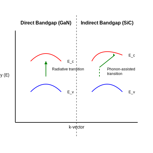
Semiconductors are classified as direct or indirect based on the momentum alignment of the valence and conduction band extrema. In a direct bandgap material (e.g., GaN), the minimum of the conduction band and maximum of the valence band occur at the same crystal momentum (k-vector), enabling efficient radiative recombination. Conversely, indirect bandgap materials (e.g., SiC) require phonon assistance for electron transitions, reducing optical efficiency.
Temperature Dependence of Bandgap
The bandgap energy is temperature-dependent due to lattice vibrations and electron-phonon coupling. The empirical Varshni equation describes this relationship:
where Eg(0) is the bandgap at 0 K, and α, β are material-specific constants. For GaN, α ≈ 0.909 meV/K and β ≈ 830 K.
Density of States and Carrier Statistics
The density of states (g(E)) in the conduction and valence bands determines the available energy states for electrons and holes. For a parabolic band approximation:
where me* is the effective electron mass. Carrier concentrations are derived from Fermi-Dirac statistics, with the intrinsic carrier density (ni) given by:
Here, Nc and Nv are the effective densities of states in the conduction and valence bands, respectively.
Practical Implications for Wide Bandgap Materials
Wide bandgap semiconductors exhibit low intrinsic carrier concentrations even at high temperatures, enabling operation in harsh environments (e.g., aerospace, power electronics). For instance, SiC devices maintain functionality at temperatures exceeding 600°C, whereas silicon-based devices degrade due to thermal generation of carriers.
Bandgap Engineering
Heterostructures (e.g., AlGaN/GaN) exploit bandgap discontinuities to confine carriers in quantum wells, enhancing mobility and optical efficiency. The Anderson rule aligns bands based on electron affinity (χ) and bandgap offsets:
This principle underpins high-electron-mobility transistors (HEMTs) and laser diodes.
1.3 Comparison with Traditional Semiconductors
Bandgap and Material Properties
Wide bandgap (WBG) semiconductors, such as silicon carbide (SiC) and gallium nitride (GaN), exhibit bandgaps significantly larger than those of traditional semiconductors like silicon (Si) and germanium (Ge). The bandgap Eg of Si is approximately 1.1 eV, while SiC and GaN have bandgaps of 3.3 eV and 3.4 eV, respectively. This fundamental difference leads to distinct electronic and thermal properties:
The larger bandgap enables WBG materials to operate at higher temperatures, withstand greater electric fields, and exhibit lower intrinsic carrier concentrations, reducing leakage currents at elevated temperatures.
Breakdown Field and Power Handling
The critical electric field Ec at which a semiconductor breaks down is directly related to its bandgap. For Si, Ec is around 0.3 MV/cm, whereas SiC and GaN exhibit breakdown fields of 2.5 MV/cm and 3.3 MV/cm, respectively. This allows WBG devices to handle higher voltages and power densities:
Consequently, WBG-based power devices can be made thinner and with higher doping concentrations, reducing on-resistance (Ron) and conduction losses.
Thermal Conductivity and Efficiency
Thermal conductivity κ is another critical parameter. SiC has a thermal conductivity of 4.9 W/cm·K, nearly three times that of Si (1.5 W/cm·K), enabling better heat dissipation. GaN, while having lower bulk thermal conductivity (1.3 W/cm·K), is often grown on high-thermal-conductivity substrates like SiC or diamond for improved thermal management.
Switching Speed and Frequency
WBG semiconductors exhibit higher electron saturation velocities (vsat), enabling faster switching speeds. For example, GaN's vsat is ~2.5×107 cm/s, compared to Si's ~1×107 cm/s. This allows high-frequency operation (>1 MHz) in power converters, reducing passive component sizes.
where Lg is the gate length. The reduced switching losses make WBG devices ideal for high-efficiency applications like electric vehicle inverters and renewable energy systems.
Practical Trade-offs and Challenges
Despite their advantages, WBG semiconductors face challenges:
- Cost: SiC and GaN wafers are more expensive than Si due to complex manufacturing processes.
- Material Defects: Dislocations and traps in epitaxial GaN layers can affect reliability.
- Gate Drive Complexity: WBG devices often require specialized gate drivers to mitigate dynamic Ron effects.
However, ongoing advances in substrate quality and device fabrication continue to address these limitations, driving adoption in high-power and high-frequency applications.
2. Gallium Nitride (GaN)
2.1 Gallium Nitride (GaN)
Gallium Nitride (GaN) is a wide bandgap semiconductor with a direct bandgap of approximately 3.4 eV, enabling superior performance in high-power, high-frequency, and high-temperature applications compared to silicon (Si) and gallium arsenide (GaAs). Its material properties stem from its wurtzite crystal structure, which contributes to high electron mobility and strong piezoelectric effects.
Crystal Structure and Electronic Properties
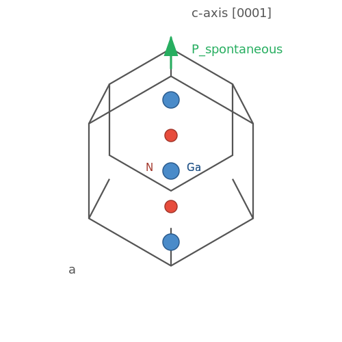
GaN crystallizes in a hexagonal wurtzite structure (space group P63mc), characterized by alternating layers of gallium and nitrogen atoms in a tetrahedral coordination. The strong ionic bonding between Ga and N atoms results in:
- High breakdown electric field (Ec ≈ 3.3 MV/cm)
- High saturation electron velocity (vsat ≈ 2.5 × 107 cm/s)
- Thermal conductivity (~130 W/m·K for bulk GaN)
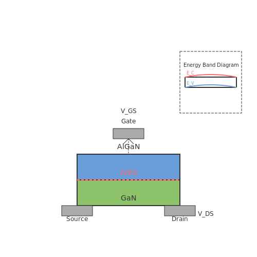
The polarization effects in GaN, both spontaneous and piezoelectric, induce a two-dimensional electron gas (2DEG) at heterojunctions (e.g., AlGaN/GaN interfaces), enabling high electron mobility transistors (HEMTs).
Key Advantages Over Silicon
GaN outperforms Si in several critical metrics:
where Eg is the bandgap and ϵs is the permittivity. GaN's wide bandgap allows for:
- Higher power density: Devices withstand voltages exceeding 600 V with lower conduction losses.
- Faster switching: Reduced parasitic capacitance enables operation at RF frequencies (up to THz).
- Thermal stability: Junction temperatures exceed 200°C without significant performance degradation.
Applications in Power Electronics
GaN is widely adopted in:
- Power converters: DC-DC and AC-DC converters achieve >99% efficiency due to low RDS(on).
- RF amplifiers: GaN HEMTs dominate 5G base stations and radar systems (L to Ka band).
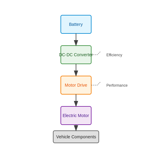
- Electric vehicles: On-board chargers and inverters benefit from compact, high-efficiency GaN modules.
Challenges in GaN Device Fabrication
Despite its advantages, GaN faces manufacturing hurdles:
- Substrate availability: Bulk GaN substrates are costly; most devices use heteroepitaxy on SiC or sapphire.
- Defect density: Dislocations (>108 cm−2) impact long-term reliability.
- Gate control: Threshold voltage instability (e.g., current collapse) requires advanced passivation techniques.
Mathematical Derivation: 2DEG Charge Density
The 2DEG sheet charge density (ns) in AlGaN/GaN HEMTs is derived from polarization mismatch and Fermi-level pinning:
where σpolarization is the net polarization charge, ϵr is the dielectric constant, and dϕb/dx is the Schottky barrier gradient.
2.2 Silicon Carbide (SiC)
Crystal Structure and Bandgap Properties
Silicon Carbide (SiC) crystallizes in multiple polytypes, with 4H-SiC and 6H-SiC being the most common for power electronics. The hexagonal close-packed (HCP) structure of 4H-SiC provides a wide bandgap of approximately 3.26 eV, significantly higher than silicon's 1.12 eV. This property enables high-temperature operation and reduced leakage currents. The bandgap energy \( E_g \) can be derived from the temperature-dependent Varshni equation:
where \( E_g(0) = 3.30 \, \text{eV} \), \( \alpha = 2.5 \times 10^{-4} \, \text{eV/K} \), and \( \beta = 820 \, \text{K} \) for 4H-SiC.
Electrical and Thermal Characteristics
SiC exhibits a critical electric field (~3 MV/cm) ten times higher than silicon, allowing thinner drift layers and lower on-resistance. The Baliga figure of merit (BFOM) quantifies its superiority for power devices:
where \( \epsilon_r \) is the relative permittivity (9.7 for SiC), \( \mu_n \) is electron mobility (~900 cm²/V·s), and \( E_c \) is the critical field. This results in a BFOM 300× higher than silicon.
Thermal conductivity reaches 4.9 W/cm·K (4H-SiC at 300K), enabling efficient heat dissipation without external cooling in high-power applications like EV inverters.
Material Growth and Fabrication Challenges
SiC substrates are grown via physical vapor transport (PVT) at temperatures exceeding 2000°C. Key challenges include:
- Micropipe defects: Hollow-core dislocations degrading breakdown voltage (now largely mitigated via improved growth techniques).
- Doping control: Nitrogen (n-type) and Aluminum (p-type) require high activation energies (~200 meV).
- Oxide reliability: SiO₂/SiC interfaces exhibit high trap densities, necessitating post-oxidation anneals in NO or N₂O.
Device Applications and Commercial Adoption
SiC enables:
- Schottky diodes: 600–1700V ratings with near-zero reverse recovery losses (Qrr).
- MOSFETs: 1200V devices with RDS(on) ≤ 25 mΩ·cm² (vs. 100+ mΩ·cm² for Si superjunction MOSFETs).
- Power modules: Wolfspeed’s 900V/300A modules in Tesla Model 3 inverters achieve 99% efficiency.
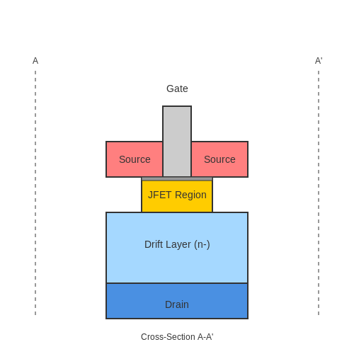
The figure below illustrates a cross-section of a SiC MOSFET, highlighting the JFET region and epitaxial drift layer:
2.3 Emerging Materials and Alloys
The development of novel wide bandgap (WBG) semiconductor materials and alloys continues to push the boundaries of power electronics, optoelectronics, and high-frequency applications. While silicon carbide (SiC) and gallium nitride (GaN) dominate current commercial WBG technologies, several emerging materials show promise for specialized applications where conventional WBG semiconductors face limitations.
Ultra-Wide Bandgap Semiconductors
Materials with bandgaps exceeding 4 eV, classified as ultra-wide bandgap (UWBG) semiconductors, enable operation at higher voltages, temperatures, and power densities than conventional WBG materials. The most prominent UWBG candidates include:
- Aluminum nitride (AlN): With a bandgap of 6.2 eV, AlN exhibits exceptional thermal conductivity (285 W/m·K) and breakdown field strength (12-15 MV/cm). Its piezoelectric properties make it ideal for RF filters and high-power ultraviolet optoelectronics.
- Diamond: Possessing the highest thermal conductivity (2200 W/m·K) and breakdown field (10-20 MV/cm) of any known material, diamond semiconductors could revolutionize extreme-environment electronics. However, challenges in n-type doping and wafer scalability remain.
- Gallium oxide (β-Ga2O3): This 4.8 eV bandgap material has attracted significant attention due to its high Baliga's figure of merit (BFOM), estimated at 3444, surpassing both SiC and GaN.
where εr is the relative permittivity, μn the electron mobility, and Ec the critical electric field.
Ternary and Quaternary Alloys
Engineered alloy systems provide tunable bandgaps and lattice constants through compositional variation:
- AlxGa1-xN: By adjusting the aluminum content (x), the bandgap can be continuously tuned from 3.4 eV (GaN) to 6.2 eV (AlN), enabling customized heterostructures for deep-UV photonics.
- InxAlyGa1-x-yN: This quaternary system allows independent control of bandgap and strain, critical for high-efficiency light-emitting diodes across the visible and UV spectrum.
- SiC-AlN alloys: Combining the high thermal conductivity of both materials, these alloys show promise for high-temperature MEMS and harsh-environment sensors.
Bandgap Engineering Considerations
The bandgap Eg of ternary alloys typically follows Vegard's law with a bowing parameter b:
For AlxGa1-xN, experimental measurements yield a bowing parameter b ≈ 1.0 eV, significantly affecting the bandgap nonlinearity at intermediate compositions.
Two-Dimensional WBG Materials
Layered materials with strong in-plane bonding and weak interlayer interactions offer unique opportunities for flexible and ultra-thin WBG devices:
- Hexagonal boron nitride (h-BN): With a 5.9 eV bandgap and atomically smooth surface, h-BN serves as an ideal substrate and gate dielectric for 2D electronics.
- Transition metal dichalcogenides (TMDs): While most TMDs are narrow-gap, materials like WS2 and MoS2 in monolayer form exhibit direct bandgaps (~2 eV) suitable for flexible optoelectronics.
Challenges in Emerging WBG Materials
Despite their theoretical advantages, several technical hurdles impede widespread adoption of these emerging materials:
- Defect density: UWBG materials like β-Ga2O3 exhibit high concentrations of point defects (1017-1019 cm-3) that degrade carrier mobility and device reliability.
- Thermal management: Materials with low thermal conductivity (e.g., β-Ga2O3 at ~10-30 W/m·K) require innovative heat extraction solutions for power electronics applications.
- Ohmic contacts: The large bandgaps of UWBG semiconductors lead to high Schottky barriers, complicating the formation of low-resistance contacts.
Recent advances in defect passivation techniques, including plasma treatments and optimized annealing processes, have shown promise in mitigating these challenges. For instance, sulfur passivation of β-Ga2O3 surfaces has demonstrated a 50% reduction in interface state density.
3. Power Electronics and Converters
3.1 Power Electronics and Converters
Wide bandgap (WBG) semiconductors, such as silicon carbide (SiC) and gallium nitride (GaN), have revolutionized power electronics by enabling higher efficiency, power density, and operating temperatures compared to traditional silicon-based devices. Their superior material properties—including higher critical electric field strength, thermal conductivity, and electron saturation velocity—make them ideal for high-frequency, high-voltage applications.
Material Advantages in Power Conversion
The breakdown electric field Ecrit of WBG materials is an order of magnitude higher than silicon, allowing thinner drift layers and reduced on-resistance. For a unipolar device like a MOSFET, the specific on-resistance Ron,sp scales with Ecrit−3:
where VBR is the breakdown voltage, ϵs the permittivity, and μn the electron mobility. This relationship enables SiC devices to achieve Ron,sp values 100–300× lower than silicon at the same voltage rating.
Switching Performance and Loss Reduction
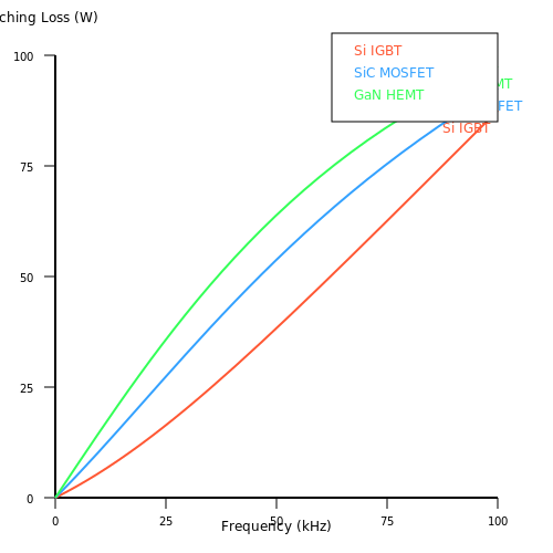
WBG devices exhibit negligible tail currents during turn-off due to the absence of minority carrier storage, reducing switching losses. The switching energy Esw in a hard-switched converter is:
where trise, tfall are transition times, and Qrr is the reverse recovery charge. GaN HEMTs, with trise as low as 2 ns, enable MHz-range switching frequencies unattainable with silicon IGBTs.
Topology Innovations Enabled by WBG Devices
The high dv/dt capability (>100 V/ns) of WBG semiconductors has spurred advances in converter topologies:
- Totem-pole PFC: GaN-based designs achieve >99% efficiency in bridgeless power factor correction circuits by eliminating diode losses.
- Multi-level converters: SiC devices enable compact 10 kV+ modular multilevel converters (MMCs) for grid applications.
- Resonant converters: LLC and CLLC topologies leverage WBG switching speeds to minimize capacitive losses at high frequencies.
Thermal Management Considerations
While WBG devices tolerate higher junction temperatures (Tj > 200°C), thermal impedance remains critical. The thermal resistance RθJC from junction to case must account for anisotropic thermal conductivity (e.g., 490 W/m·K in-plane for 4H-SiC vs. 3 W/m·K cross-plane):
Advanced packaging techniques like silver sintering and double-sided cooling are often employed to maximize heat extraction.
Real-World Implementation Challenges
Despite their advantages, WBG power modules require careful attention to:
- Gate drive design: Negative voltage bias (-3 to -5 V) is often needed to prevent spurious turn-on due to high dv/dt.
- Parasitic inductance: Layouts must minimize Ls (<1 nH) to avoid voltage overshoot during switching transitions.
- EMI mitigation: The fast edges necessitate optimized snubber circuits and shielding strategies.
3.2 High-Frequency Devices
Wide bandgap (WBG) semiconductors, such as gallium nitride (GaN) and silicon carbide (SiC), exhibit superior high-frequency performance compared to silicon due to their high critical electric field and electron saturation velocity. These properties enable devices like high-electron-mobility transistors (HEMTs) and Schottky diodes to operate efficiently at microwave and millimeter-wave frequencies.
Key High-Frequency Parameters
The performance of high-frequency WBG devices is governed by several critical parameters:
- Cutoff Frequency (fT): The frequency at which current gain drops to unity. For GaN HEMTs, fT can exceed 100 GHz due to high electron mobility in the two-dimensional electron gas (2DEG) channel.
- Maximum Oscillation Frequency (fmax): The frequency at which power gain becomes unity, influenced by gate resistance and parasitic capacitances.
- Output Power Density: WBG devices achieve power densities >5 W/mm at X-band frequencies, far surpassing silicon-based devices.
GaN HEMTs for RF Applications
GaN-based HEMTs dominate high-power RF applications due to their high breakdown voltage and thermal stability. The AlGaN/GaN heterostructure forms a 2DEG with sheet carrier densities ~1013 cm-2 and mobility >1500 cm2/V·s. The current-voltage relationship in the saturation region is given by:
where μn is electron mobility, Cox is oxide capacitance, and λ is channel-length modulation parameter. The high fT results from the short transit time (τt) across the channel:
where vsat is the saturation velocity (~2×107 cm/s for GaN) and Lg is gate length.
Parasitic Effects and Mitigation
At high frequencies, parasitic elements significantly impact performance:
- Gate Resistance (Rg): Reduced through T-gate or Γ-gate structures, lowering noise figure.
- Source Inductance (Ls): Minimized via via-hole grounding, improving fmax.
- Current Collapse: Addressed with field plates or passivation layers to suppress surface traps.
High-Frequency Circuit Applications
WBG devices enable transformative RF systems:
- 5G Power Amplifiers: GaN PA modules deliver >40% efficiency at 28 GHz with 8 dB gain.
- Radar Systems: X-band GaN MMICs achieve 50 W output power with 60% duty cycle.
- Millimeter-Wave Backhaul: E-band (71-76 GHz) transceivers using WBG devices support 10 Gbps links.
Recent advances in diamond substrates and lateral GaN-on-diamond HEMTs have pushed fmax beyond 300 GHz, opening terahertz applications. Thermal management remains critical, with thermal resistances <1.5 K·mm/W required for reliable operation.
3.3 Optoelectronic Applications
Wide bandgap (WBG) semiconductors, such as gallium nitride (GaN), silicon carbide (SiC), and aluminum nitride (AlN), exhibit superior optoelectronic properties due to their direct bandgaps, high breakdown fields, and thermal stability. These materials are pivotal in high-efficiency light-emitting diodes (LEDs), laser diodes (LDs), photodetectors, and ultraviolet (UV) optoelectronic systems.
High-Efficiency Light-Emitting Diodes (LEDs)
GaN-based LEDs dominate solid-state lighting due to their high quantum efficiency and wavelength tunability. The radiative recombination rate in WBG semiconductors is governed by:
where ηint is the internal quantum efficiency and ηextraction is the light extraction efficiency. The bandgap energy (Eg) determines the emission wavelength:
For instance, InGaN alloys enable emission from near-UV (3.4 eV) to green (2.3 eV), while AlGaN extends into deep-UV (≤280 nm).
Laser Diodes (LDs)
WBG LDs achieve high-power, short-wavelength operation critical for optical storage, projection, and medical applications. The threshold current density (Jth) is minimized by optimizing carrier confinement and reducing defect densities:
where d is the active layer thickness, ηi is the injection efficiency, τr is the radiative lifetime, αi is the internal loss, and R1, R2 are mirror reflectivities.
UV Photodetectors
AlGaN-based photodetectors exhibit solar-blind operation (200–280 nm), essential for flame sensing and UV astronomy. The responsivity (R) is given by:
where η is the quantum efficiency. High defect tolerance in WBG materials reduces dark current, enhancing signal-to-noise ratios.
Challenges and Innovations
Despite their advantages, WBG optoelectronics face challenges such as:
- P-type doping limitations in Al-rich AlGaN due to high activation energies.
- Lattice mismatch in heterostructures, necessitating buffer layers or strain engineering.
- Thermal droop in high-power LEDs, mitigated by nanostructured active regions.
Recent advances include polarization-engineered heterojunctions and tunnel junctions to circumvent doping constraints, as well as photonic crystal designs for enhanced light extraction.
4. Performance Benefits
4.1 Performance Benefits
Higher Breakdown Field and Power Density
Wide bandgap (WBG) semiconductors such as SiC and GaN exhibit significantly higher critical electric field strengths compared to silicon. The breakdown field Ec scales with bandgap energy Eg as:
For 4H-SiC (Eg = 3.26 eV), this results in a breakdown field ~10× higher than silicon (1.12 eV). Consequently, WBG devices achieve:
- Thinner drift layers (reduced by 10× for same voltage rating)
- Higher doping concentrations (increased by 100×)
- 5-10× lower specific on-resistance (Ron,sp)
Superior Thermal Conductivity
4H-SiC's thermal conductivity (3.7 W/cm·K) is 3× higher than silicon, enabling:
- Higher power density operation (500 W/cm² vs. 150 W/cm² for Si)
- Reduced heatsink requirements
- Improved reliability at high temperatures
High-Temperature Operation
WBG materials maintain performance at junction temperatures exceeding 200°C due to:
- Lower intrinsic carrier concentration (ni):
- Reduced thermal generation of carriers
- Stable material properties at elevated temperatures
Reduced Switching Losses
The combination of high electron saturation velocity (vsat) and low parasitic capacitances enables:
- Ultra-fast switching (GaN HEMTs: <100 ns transition times)
- Lower reverse recovery losses (SiC Schottky diodes: Qrr ≈ 0)
High-Frequency Capability
WBG devices achieve switching frequencies >1 MHz due to:
- Reduced energy storage in drift regions
- Lower gate charge requirements
- Minimal minority carrier storage effects
This enables compact passive components in power converters, as seen in 99% efficient 1 MHz GaN-based LLC resonant converters.
Radiation Hardness
The strong covalent bonds in WBG materials provide:
- Higher displacement energy thresholds (20-35 eV vs. 12.8 eV for Si)
- Reduced degradation in space and nuclear applications
4.2 Thermal and Electrical Stability
Wide bandgap (WBG) semiconductors, such as SiC and GaN, exhibit superior thermal and electrical stability compared to traditional silicon-based devices. This stability arises from their high critical electric field strength, thermal conductivity, and intrinsic material properties.
Thermal Stability
The thermal stability of WBG materials is governed by their high thermal conductivity (κ) and melting points. For example, SiC has a thermal conductivity of ~490 W/m·K at room temperature, compared to ~150 W/m·K for silicon. The heat dissipation capability is derived from the phonon transport properties, described by:
where Cv is the heat capacity, vs is the speed of sound, and ℓ is the phonon mean free path. The high κ minimizes thermal resistance, reducing hot-spot formation in high-power applications.
Electrical Stability
WBG semiconductors maintain electrical stability under high electric fields due to their wide bandgap (Eg). The critical electric field (Ecrit) before breakdown is approximated by:
where q is the electron charge and ϵs is the permittivity. For SiC (Eg ≈ 3.3 eV), Ecrit reaches ~3 MV/cm, enabling thinner drift layers and lower conduction losses.
Reliability Under High-Temperature Operation
WBG devices demonstrate stable performance at elevated temperatures (>200°C), where silicon devices degrade. Key mechanisms include:
- Reduced intrinsic carrier concentration (ni): $$ n_i = \sqrt{N_c N_v} e^{-E_g / 2kT} $$ suppresses leakage currents.
- Lower thermal expansion mismatch: SiC and GaN have coefficients closer to common substrate materials (e.g., AlN), reducing mechanical stress.
Practical Implications
In power electronics, WBG devices enable:
- Higher switching frequencies (>100 kHz) with minimal thermal derating.
- Improved reliability in harsh environments (e.g., aerospace, automotive).
- Reduced cooling requirements due to lower junction temperatures.
For example, GaN HEMTs in RF amplifiers maintain efficiency at high power densities (>10 W/mm) without thermal runaway, a limitation in silicon LDMOS devices.
4.3 Manufacturing and Cost Challenges
Wide bandgap (WBG) semiconductors, such as silicon carbide (SiC) and gallium nitride (GaN), offer superior electrical properties compared to silicon, but their manufacturing presents significant technical and economic hurdles. The primary challenges stem from material synthesis, defect control, and substrate availability, all of which contribute to higher production costs.
Material Synthesis and Crystal Growth
The synthesis of high-quality WBG materials requires extreme conditions due to their high melting points and chemical stability. For SiC, the modified Lely method (sublimation growth) is commonly used, but achieving low defect densities remains difficult. The process involves temperatures exceeding 2000°C, with precise control of vapor-phase stoichiometry to minimize micropipes and dislocations. GaN, typically grown heteroepitaxially on substrates like sapphire or silicon, suffers from lattice mismatch-induced defects, necessitating complex buffer layers.
where Δa/a0 is the lattice mismatch ratio, Ea is the activation energy for defect formation, and T is the growth temperature.
Substrate Limitations
SiC substrates account for nearly 50% of device costs due to slow growth rates (~0.2–0.5 mm/hr) and energy-intensive processes. While 150-mm wafers are emerging, most production still relies on 100-mm wafers, limiting economies of scale. GaN faces similar challenges, with bulk GaN substrates being prohibitively expensive, forcing reliance on foreign substrates that degrade device performance.
Fabrication Complexity
WBG devices require specialized processing steps:
- High-temperature ion implantation: Dopant activation in SiC demands annealing at 1600–1700°C, incompatible with standard silicon fab equipment.
- Etching challenges: SiC’s chemical inertness necessitates plasma etching with fluorine-based chemistries, increasing tool wear and process variability.
- Gate dielectrics: Interface traps at SiO2/SiC boundaries reduce channel mobility, requiring advanced passivation techniques.
Cost Drivers and Market Dynamics
Despite a 30% annual reduction in SiC wafer costs since 2010, prices remain 5–10× higher than silicon equivalents. Key cost contributors include:
| Factor | SiC | GaN-on-Si |
|---|---|---|
| Substrate cost | $$500–$$800/wafer | $$100–$$200/wafer |
| Epitaxy | 20–30% of total cost | 40–50% of total cost |
| Yield loss | 15–25% | 10–20% |
Automotive and industrial applications are driving volume production, with 200-mm wafer adoption expected to reduce costs by 40% by 2026. However, achieving defect densities below 0.1 cm−2 remains critical for high-voltage devices.
5. Advances in Material Science
5.1 Advances in Material Science
Wide bandgap (WBG) semiconductors, such as silicon carbide (SiC) and gallium nitride (GaN), have undergone significant material science advancements, enabling their dominance in high-power, high-frequency, and high-temperature applications. The key breakthroughs lie in defect reduction, doping control, and epitaxial growth techniques.
Crystal Growth and Defect Engineering
The primary challenge in WBG semiconductors has been minimizing defects like micropipes in SiC and threading dislocations in GaN. Modified physical vapor transport (PVT) for SiC and metal-organic chemical vapor deposition (MOCVD) for GaN have achieved defect densities below 103 cm-2. The introduction of step-controlled epitaxy for SiC and the use of aluminum nitride (AlN) buffer layers for GaN on silicon substrates have been pivotal.
where Ddefect is the defect density, Ea is the activation energy for defect formation, and T is the growth temperature.
Doping Asymmetry and Mobility Enhancement
WBG materials exhibit strong doping asymmetry—n-type doping is straightforward (nitrogen for GaN, nitrogen/phosphorus for SiC), while p-type doping remains challenging (magnesium for GaN, aluminum for SiC). Recent advances include:
- Site-competition epitaxy for precise doping control in SiC
- Modulation doping in AlGaN/GaN heterostructures achieving 2D electron gas mobility >2000 cm2/V·s
- Hybrid beam epitaxy for oxygen-free Ga2O3 with controlled silicon doping
Thermal Management Innovations
The high power densities in WBG devices demand advanced thermal solutions. Diamond substrates with thermal conductivity >2000 W/m·K are now integrated via:
- Wafer bonding with nanoscale surface activation
- Direct diamond growth on GaN using iridium interlayers
- Patterned graphene thermal vias in SiC power modules
Novel Material Systems
Emerging ultra-wide bandgap materials (>4.5 eV) are pushing boundaries:
| Material | Bandgap (eV) | Breakdown Field (MV/cm) |
|---|---|---|
| β-Ga2O3 | 4.8 | 8 |
| AlN | 6.2 | 15 |
| Diamond | 5.5 | 20 |
β-Ga2O3 has demonstrated Baliga's figure of merit (BFOM) 10× higher than SiC, with recent edge-terminated Schottky diodes achieving 8 kV breakdown.
where εr is relative permittivity, μn is electron mobility, and Ec is critical electric field.
Heterogeneous Integration
Monolithic integration of WBG materials with silicon CMOS has enabled new device architectures. Key developments include:
- GaN-on-Si RFICs with ft/fmax >100 GHz
- 3D-integrated SiC IGBTs with through-silicon vias (TSVs)
- GaN/SiC hybrid modules for 99.3% efficient 10 kV converters
5.2 Integration with Existing Technologies
The adoption of wide bandgap (WBG) semiconductors such as silicon carbide (SiC) and gallium nitride (GaN) into existing power electronic systems presents both opportunities and challenges. Their superior material properties—including higher breakdown voltages, faster switching speeds, and lower conduction losses—necessitate careful consideration when interfacing with conventional silicon (Si)-based components.
Compatibility with Silicon-Based Systems
WBG devices often operate at higher voltages and temperatures than Si components, requiring modifications to gate drive circuits, thermal management, and passive components. The threshold voltage (Vth) of SiC MOSFETs, for example, typically ranges from 2–4 V, whereas Si MOSFETs may have thresholds as low as 1 V. This difference necessitates adjusted gate driver designs to ensure reliable turn-on and avoid spurious switching events.
where ΔVmargin accounts for noise immunity and process variations. Under-driving the gate can lead to increased conduction losses, while overdriving may accelerate gate oxide degradation.
Parasitic Considerations in Hybrid Systems
The fast switching transitions of WBG devices (with dv/dt exceeding 100 V/ns) exacerbate parasitic inductance and capacitance effects in PCB layouts. Stray inductances in source and gate loops can induce voltage spikes, given by:
To mitigate this, designers must minimize loop areas, use low-inductance packaging (e.g., Kelvin connections), and often incorporate snubber circuits or active clamping techniques.
Thermal Management in Mixed-Technology Modules
While SiC and GaN devices can operate at junction temperatures exceeding 200°C, traditional solder interconnects and wire bonds may degrade under prolonged thermal cycling. Advanced packaging solutions such as silver sintering or double-sided cooling become critical when integrating WBG devices into existing power modules originally designed for Si IGBTs.
The thermal resistance network must be re-evaluated to account for the higher power densities:
where ti, ki, and Ai represent thickness, thermal conductivity, and cross-sectional area of each layer in the stack-up.
EMI and Filtering Challenges
The high-frequency switching of WBG devices shifts EMI spectra toward higher bands, often requiring redesign of input filters. Common-mode noise becomes particularly problematic due to capacitive coupling through heat sinks. The displacement current can be approximated by:
where Chs is the heat sink capacitance. Solutions include using isolated baseplates, adding common-mode chokes with higher frequency ratings, and optimizing transformer interwinding capacitance in isolated converters.
Control System Implications
Digital controllers designed for Si devices may lack the resolution needed to fully exploit WBG switching speeds. For example, a 100 MHz PWM clock provides only 10 ns resolution—comparable to the rise times of GaN HEMTs. This demands either higher clock speeds or time-interleaved control techniques to prevent limit cycling and subharmonic oscillations.
The minimum achievable dead time (td,min) becomes constrained by propagation delays:
where tprop terms account for signal propagation through gate drivers and current sensors, and tcomp represents comparator response time.
Case Study: SiC/Si Hybrid Inverter
A practical implementation in electric vehicle traction inverters often uses SiC MOSFETs for the high-voltage stage (≥ 600 V) while retaining Si IGBTs for lower voltage auxiliary circuits. This hybrid approach balances performance and cost, but requires:
- Synchronized gate timing to prevent shoot-through
- Adaptive voltage scaling for mixed-voltage domains
- Asymmetric thermal design to accommodate differing loss profiles
5.3 Sustainability and Environmental Impact
The adoption of wide bandgap (WBG) semiconductors, such as silicon carbide (SiC) and gallium nitride (GaN), presents significant sustainability advantages over traditional silicon-based devices. Their superior material properties enable higher energy efficiency, reduced thermal losses, and longer operational lifetimes, directly contributing to lower carbon emissions in power electronics applications.
Energy Efficiency and Carbon Footprint Reduction
The primary environmental benefit of WBG semiconductors stems from their reduced conduction and switching losses. The bandgap energy (Eg) of SiC (3.26 eV) and GaN (3.4 eV), compared to silicon (1.12 eV), allows operation at higher temperatures, voltages, and frequencies with lower energy dissipation. The power loss reduction can be quantified through the figure of merit (FOM) for switching devices:
where Ron is the specific on-resistance and Qg is the gate charge. WBG devices typically achieve FOM values 5-10× lower than silicon counterparts. In practical terms, this translates to 30-50% reduction in energy losses in applications like:
- Electric vehicle power inverters
- Renewable energy systems (solar/wind converters)
- Industrial motor drives
Material and Manufacturing Considerations
While WBG devices offer operational energy savings, their production involves more energy-intensive processes. SiC crystal growth requires temperatures exceeding 2000°C, compared to silicon's 1420°C. The environmental impact can be assessed through life cycle analysis (LCA) metrics:
Studies indicate that for a 1 MW photovoltaic inverter, SiC-based systems achieve CO2 payback within 2-3 years of operation, with net savings exceeding 500 tons of CO2 over a 20-year lifespan.
Resource Availability and Recycling
Gallium and silicon carbide face different sustainability challenges:
| Material | Abundance | Recyclability |
|---|---|---|
| GaN | Gallium: 19 ppm in Earth's crust (by-product of aluminum/zinc production) | Limited recycling infrastructure, but chemically stable for long-term use |
| SiC | Silicon: 28% of Earth's crust, Carbon: 0.02% | High chemical stability enables potential reuse in abrasive applications |
End-of-Life Management
The extreme durability of WBG materials presents both advantages and challenges. While their long operational life reduces replacement frequency, the same properties make them resistant to conventional recycling methods. Emerging techniques include:
- Electrochemical etching for GaN recovery
- High-temperature pyrolysis for SiC substrate reclamation
- Selective area regrowth for wafer reuse
Current research focuses on developing circular economy models for WBG semiconductors, where up to 85% of the original wafer material could be reclaimed through advanced recycling processes.
6. Key Research Papers
6.1 Key Research Papers
- An overview of wide and ultra wide bandgap semiconductors for next ... — The emerging wide bandgap technology is a key enabler, offering better efficiency, power density, switching speed, and reduced size and weight. In view of this, we present an extensive overview of wide bandgap and ultra-wide bandgap devices for present & next-generation power electronics applications.
- (PDF) Extreme Implementations of Wide-Bandgap Semiconductors in Power ... — The emergence of wide bandgap power semiconductor devices has opened the possibilities of improved electrical performance and power density. Advanced research into wide bandgap power electronics also includes advances in integrated circuit design, semiconductor device modeling, 3D electronic packaging, and computer-aided design of wide bandgap ...
- PDF Barriers to the Adoption of Wide-Bandgap Semiconductors for Power ... — Abstract—Wide-bandgap power semiconductor devices offer enormous energy efficiency gains in a wide range of potential applications. As silicon-based semiconductors are fast ap-proaching their performance limits for high power require-ments, wide-bandgap semiconductors such as gallium nitride and silicon carbide with their superior electrical properties are likely candidates to replace ...
- Outlook of Wide-Bandgap Semiconductors and Power Electronics in the ... — The chapter also covers future research and development directions in materials science, characterization, and physical electronic device architectures to push the limits of power electronics to utilize wide-bandgap semiconductors that go beyond Si and SiC.
- Wide-bandgap semiconductors and power electronics as pathways ... - Nature — This paper reviews the electromagnetic interference challenges, methods and solutions for high-frequency and high-speed power electronics systems based on wide-bandgap power semiconductors.
- PDF Wide Bandgap Semiconductors - download.e-bookshelf.de — As described in Sect. 1.2, other important wide bandgap semiconductors such as silicon carbide and diamond are being studied for electronic device applications.
- Power Electronics Revolutionized: A Comprehensive Analysis of ... - MDPI — This article provides a comprehensive review of wide and ultrawide bandgap power electronic semiconductor devices, comparing silicon (Si), silicon carbide (SiC), gallium nitride (GaN), and the emerging device diamond technology. Key parameters examined include bandgap, critical electric field, electron mobility, voltage/current ratings, switching frequency, and device packaging. The historical ...
- PDF Wide Bandgap (WBG) Semiconductors in Power Electronics: — In summary, the nuances between gallium nitride and silicon carbide semiconductors highlight their respective roles in EV technology, with SiC's temperature resistance making it an essential component of long-term durability and stability, and GaN's high-frequency performance making it a key element of fast-charging technology, reflecting the ...
- PDF Review of wide band gap chalcogenide semiconductors — This manuscript provides a review of wide band gap chalcogenide semiconductors. First, we outline general materials design parameters of high performing transparent conductors, as well as the theoretical and experimental underpinnings of the corresponding research methods.
- Wide band gap semiconductor technology: State-of-the-art — The superb materials properties of wide band gap semiconductors have promise of enabling orders of magnitude better performance than has already been achieved. Realizing this dream requires a deeper understanding of the device physics and physics based new approaches to materials and device technology.
6.2 Industry Reports and White Papers
- Wide Bandgap Semiconductors Market Size & Trends 2022-2032 — Wide Bandgap Semiconductors Market Outlook (2022 to 2032) The global wide bandgap semiconductor market is forecasted to be valued at USD 831.8 million by 2032, up from USD 241.3 million in 2022, advancing at a CAGR of 13.2% during the forecast period.
- Wide Bandgap Semiconductors Market By Material (Silicon Carbide ... — Wide Bandgap Semiconductors Market By Material (Silicon Carbide, Gallium Nitride, Diamond, Others), By Industry Vertical : Global Opportunity Analysis and Industry Forecast, 2023-2032 - According to a new report published by Allied Market Research, titled, "Wide Bandgap Semiconductors Market," The wide bandgap semiconductors market was valued at $1.6 billion in 2022, and is estimated to reach ...
- Wide Bandgap Semiconductors Market - Industry Analysis Forecast — The Wide Bandgap Semiconductors Market size was valued at USD 1.70 Billion in 2023 and the total Wide Bandgap Semiconductors revenue is expected to grow at a CAGR of 12.6% from 2024 to 2030, reaching nearly USD 3.91 Billion. The report includes the analysis of the impact of COVID-19 lockdown on the revenue of market leaders, followers, and disruptors.
- A Review of Wide Bandgap Semiconductors: Insights into SiC, IGZO, and ... — In comparison, the development of ultra-wide bandgap semiconductors like gallium oxide (Ga₂O₃) and aluminum nitride (AlN), which possess bandgaps of 4.9 eV and 6.2 eV and offer superior power densities and lower energy losses, is significantly hindered by a lack of effective p-type doping [116,117,118]. This limitation confines their ...
- Ultrawide-bandgap semiconductors: An overview | Journal of Materials ... — Ultrawide-bandgap (UWBG) semiconductors, with bandgap energies much greater than the 3.4 eV of GaN or 3.2 eV of SiC, represent an emerging new area of intensive research covering a wide spectrum of materials, physics, devices, and applications [].As the critical electric field of avalanche breakdown increases super-linearly with increasing bandgap energy (detailed analysis discussed in a ...
- PDF Comparison of Wide-bandgap Semiconductors for Power Electronics ... — New semiconductor materials called wide-bandgap (WBG) semiconductors, such as silicon carbide (SiC), gallium nitride (GaN), and diamond, are possible candidates for replacing Si in transportation applications. The next sections will discuss why wide-bandgap semiconductor-based power devices are required for transportation applications. 1.1 ...
- PDF Wide Bandgap (WBG) Semiconductors in Power Electronics: — Wide Bandgap (WBG) Semiconductors in Power Electronics: The Future of Electric Vehicles Bachelor's thesis 2024 39 pages,7 figures,1table Examiner(s): Associate Professor Lassi Aarniovuori Keywords: electric vehicles, broadband semiconductors, gallium nitride, silicon carbide, energy efficiency, autonomy
- Ultrawide‐Bandgap Semiconductors: Research Opportunities and Challenges ... — The critical electric field, in turn, scales approximately as the square of the semiconductor bandgap, so the BFOM scales approximately as the sixth power of the semiconductor bandgap. In other words, moving from GaN to AlN gives an increase in bandgap by a factor of 1.8 ≈ 6.0 eV/3.4 eV, but a nonlinear increase in the BFOM of ≈ 34 ≈ (1.8) 6.
- Emerging trends in wide band gap semiconductors (SiC and GaN ... — Among the wide band gap (WBG) semiconductors, silicon carbide (4H-SiC) and gallium nitride (GaN) are nowadays recognized as outstanding materials for the future of power electronics. In fact, owing to their excellent properties, they can guarantee a better energy efficiency in power conversion systems with respect to Silicon.
- From wide to ultrawide-bandgap semiconductors for high power and high ... — In this comprehensive review article, our primary focus is on the exploration of electronic device technology led by GaN as a well-established technology, along with emerging technologies such as AlGaN/AlN, Diamond, and β-Ga 2 O 3.Our discussion will revolve around various aspects of these materials of interest, including their material properties, growth techniques, devices, and applications ...
6.3 Recommended Books and Courses
- Wide Bandgap Semiconductors for Power Electronics: Materials, Devices ... — Wide Bandgap Semiconductors for Power Electronic A guide to the field of wide bandgap semiconductor technology Wide Bandgap Semiconductors for Power Electronics is a comprehensive and authoritative guide to wide bandgap materials silicon carbide, gallium nitride, diamond and gallium (III) oxide. With contributions from an international panel of experts, the book offers detailed coverage of the ...
- Wide Bandgap Semiconductors for Power Electronics: Materials, Devices ... — Meets the demand for a resource that addresses wide bandgap materials in a comprehensive manner Written for materials scientists, semiconductor physicists, electrical engineers, Wide Bandgap Semiconductors for Power Electronics provides a state of the art guide to the technology and application of SiC and related wide bandgap materials.
- Optical Properties and Electronic Structure of Wide Band Gap II-VI ... — 4.4 Band Gap Values of Binary Wurzite II-VI Semiconductors 4.5 Reference Values for the Band Gap of II-VI Wide Band Gap Semiconductors 4.6 Band Gap Modification by Strain 4.6.1 Strain Due to Lattice Mismatch and Differential Thermal Expansion 4.6.2 Modification of the Electronic Band Structure by Strain 5 Band Gap of Semiconductor Alloys 5.1
- Wide Bandgap Semiconductors: Fundamental Properties and Modern Photonic ... — This book offers a comprehensive overview of the development, current state and future prospects of wide bandgap semiconductor materials and related optoelectronics devices. It includes an overview of recent developments in III-V nitride semiconductors, SiC, diamond, ZnO, II-VI materials and related devices including AIGaN/GaN FET, UV LDs, white light LEDs, and cold electron emitters. With 901 ...
- Wide Bandgap Semiconductors for Power Electronics [Book] — The book is filled with the most recent developments in the burgeoning field of wide bandgap semiconductor technology and includes information from cutting-edge semiconductor companies as well as material from leading universities and research institutions.
- GaN/SiC based High Electron Mobility Transistors for integrated ... — Wide bandgap semiconductors show great promise for advancing the state-of-the-art for high power microwave electronic devices. Recent improvements in the growth of wide bandgap semiconductor materials, such as SiC and the GaN-based alloys, provide the opportunity to design and fabricate microwave transistors that demonstrate performance ...
- PDF Wide Bandgap (WBG) Semiconductors in Power Electronics: — It is concluded that although gallium nitride and silicon carbide semiconductor technologies have great potential for application in the electric vehicle industry, further research and development in the areas of cost control, supply chain management and technology standardisation are required to achieve commercialisation and scale-up of these ...
- Gallium Nitride and Silicon Carbide Power Devices — It can be used as a reference by practicing engineers in the power electronics industry and as a textbook for a power device or power electronics course in universities. Readership: Researchers, academics, and graduate students in electrical & electronic engineering, semiconductors, materials engineering and energy research.
- PDF Wide Bandgap Semiconductor Opportunities in Power Electronics — Wide Bandgap Semiconductor Opportunities in Power Electronics Kristina Armstrong Sujit Das Laura Marlino November 2017 Approved for public release.
- PDF Fundamentals of Semiconductors: Physics and Materials Properties, 4th ... — The best-known semiconductor is of course the element Si. Together with ger- manium (Ge), it is the prototype of a large class of semiconductors with sim- ilar crystal structures.