


Gain amplifying circuit diagram or programming

Description: The PGA103 is designed with a wide input voltage range. It utilizes a voltage divider circuit consisting of a 11.3kΩ resistor and a 102kΩ resistor, achieving a division ratio of approximately 1/10. For instance, when the input voltage is 120V, the voltage applied to the PGA103 is reduced to 12V, enabling the amplifier to handle a wide input voltage range. Additionally, diodes D1 and D2 (1N4148) provide a bidirectional clamping function, limiting the input voltage to the PGA103 to a range of 15V to -0.7V.
The PGA103 operational amplifier is specifically engineered to accommodate a broad spectrum of input voltages, making it suitable for various applications where high voltage signals need to be processed. The implementation of a voltage divider using an 11.3kΩ resistor in conjunction with a 102kΩ resistor allows for precise scaling down of high input voltages. This configuration ensures that when subjected to a high input voltage, such as 120V, the resultant voltage presented to the PGA103 is safely reduced to 12V, thereby preventing damage to the amplifier and ensuring proper operation.
The choice of diodes D1 and D2, specifically the 1N4148 model, is critical for protecting the PGA103 from voltage spikes and reverse polarity conditions. These diodes are configured in a bidirectional arrangement to clamp the input voltage effectively, ensuring that the operational amplifier receives a maximum input voltage of 15V and a minimum of -0.7V. This clamping mechanism is essential for safeguarding the integrity of the PGA103's internal circuitry and maintaining its performance characteristics over varying input conditions.
Overall, the combination of the voltage divider and the clamping diodes plays a pivotal role in the reliable operation of the PGA103 in high-voltage environments, making this circuit design a robust solution for interfacing with high-voltage signals. As shown in FIG PGA103 constituted by a wide input voltage range of the amplifier. 11.3k with 102k resistor voltage divider circuit dividing ratio of about 1/10, such as when t he input voltage is 120V, after dividing the input voltage applied PGA103 only 12V, wide input voltage can be. At the same time, the diode D1, D2 (take 1N4148) play a two-way clamping action, PGA103 input voltage of 15 ~ disabilities 0.7V.
The PGA103 operational amplifier is specifically engineered to accommodate a broad spectrum of input voltages, making it suitable for various applications where high voltage signals need to be processed. The implementation of a voltage divider using an 11.3kΩ resistor in conjunction with a 102kΩ resistor allows for precise scaling down of high input voltages. This configuration ensures that when subjected to a high input voltage, such as 120V, the resultant voltage presented to the PGA103 is safely reduced to 12V, thereby preventing damage to the amplifier and ensuring proper operation.
The choice of diodes D1 and D2, specifically the 1N4148 model, is critical for protecting the PGA103 from voltage spikes and reverse polarity conditions. These diodes are configured in a bidirectional arrangement to clamp the input voltage effectively, ensuring that the operational amplifier receives a maximum input voltage of 15V and a minimum of -0.7V. This clamping mechanism is essential for safeguarding the integrity of the PGA103's internal circuitry and maintaining its performance characteristics over varying input conditions.
Overall, the combination of the voltage divider and the clamping diodes plays a pivotal role in the reliable operation of the PGA103 in high-voltage environments, making this circuit design a robust solution for interfacing with high-voltage signals. As shown in FIG PGA103 constituted by a wide input voltage range of the amplifier. 11.3k with 102k resistor voltage divider circuit dividing ratio of about 1/10, such as when t he input voltage is 120V, after dividing the input voltage applied PGA103 only 12V, wide input voltage can be. At the same time, the diode D1, D2 (take 1N4148) play a two-way clamping action, PGA103 input voltage of 15 ~ disabilities 0.7V.

Regulated voltage divider
Integrated circuits (ICs) that require 3 or 6 volts can be powered from a battery or a fixed regulated supply with a higher voltage using the circuit illustrated. It is essential to mount the transistor on a heatsink, as significant...

Reading a voltage divider schematic
Ground serves as a reference point for the voltage divider, with each successive point above ground indicating the voltage drop across the circuit. For example, with a 15-volt input and 5K ohm resistors, the voltage taps would measure 5, 10,...

Constituted by the PGA103 programmable gain instrumentation amplifier circuit diagram
The circuit depicted in the figure comprises a PGA103 programmable gain instrumentation amplifier. This design utilizes the PGA205 and PGA103 in a cascading configuration, resulting in a total gain for the amplifier. The gain is determined by the product of...

autoconnect disconnect battery charger
A simple battery charger is designed to disconnect the battery when the charge voltage reaches its nominal level and reconnect when the battery voltage drops below a predefined threshold. This is achieved using a circuit diagram that incorporates a voltage...
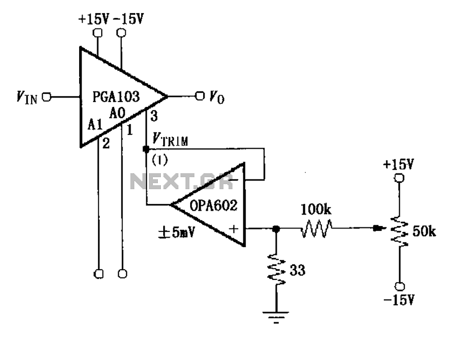
PGA103 offset voltage correction circuit diagrams
The PGA103 offset voltage correction circuit is designed to minimize the offset voltage for the PGA103 laser correction, ensuring that the gain for three typical offset voltage levels (relative to input) remains below 200 V. Each gain is associated with...
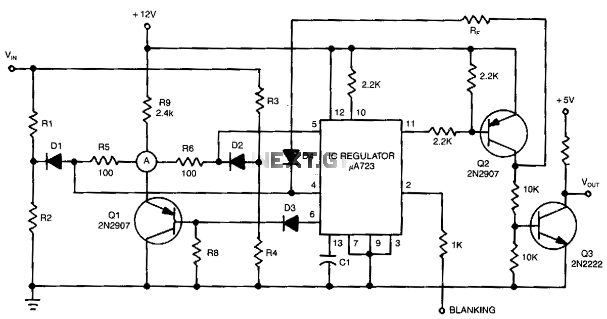
Window-detector
The detector circuit compares the output voltage of two separate voltage dividers with a fixed reference voltage. The resultant absolute error signal is amplified and converted to a logic signal that is TTL compatible.
The described detector circuit serves as a...

Circuit clarification needed
Can someone please help explain how this circuit works? I am confident that I understand how the voltage divider network operates.
The circuit in question likely includes a voltage divider configuration, which is a fundamental concept in electronics used to produce...

When use Voltage divider in circuit analysis
The Delta configuration of resistors R2, R3, and R4 is converted to a Wye (Y) configuration. This conversion is necessary because a voltage divider is typically employed in series circuits. The aim is to determine the total resistance in this...