


HS-3182 ARINC 429 Bus Interface Line Driver Circuit
#ARINC 429
#bus interface
#line driver
#data formatting
#TTL compatible
#CMOS compatible
#telecommunication
#differential line driver
#monolithic
#bipolar

Description: The HS-3182 is a monolithic dielectrically isolated bipolar differential line driver designed to meet the specifications of ARINC 429. This device is intended to be used with a companion chip, the HS-3282 CMOS ARINC Bus Interface Circuit, which provides data formatting and processor interface functions. All logic inputs are compatible with TTL and CMOS standards. In addition to the DATA (A) and DATA (B) inputs, there are also inputs for CLOCK and SYNC signals that are ANDed with the DATA inputs. This feature enhances system performance and allows the HS-3182 to be utilized with devices other than itself. Three power supplies are required for the operation of the HS-3182: +V = +15V ±10%, -V = -15V ±10%, and V1 = 5V ±5%. VREF is used to program the differential output voltage swing such that VOUT (DIFF) = ±2VREF. Typically, VREF is set to V1 = 5V ±5%, but a separate power supply may be used for VREF, which should not exceed 6V. The driver output impedance is 75 ±20% at +25 °C. The rise and fall times of the driver output are independently programmable through the use of two external capacitors connected to the CA and CB inputs. Typical capacitor values are CA = CB = 75pF for high-speed operation (100kBPS), and CA = CB = 300pF for low-speed operation (12kBPS to 14.5kBPS). The outputs are protected against overvoltage and short circuits as illustrated in the block diagram. The HS-3182 is designed to operate over an ambient temperature range of -55 °C to +125 °C, or -40 °C to +85 °C.
The HS-3182 differential line driver is engineered to facilitate reliable data transmission in environments adhering to ARINC 429 specifications, commonly used in avionics systems. The dielectrically isolated design ensures that the driver maintains signal integrity while minimizing noise and interference. The integration of TTL and CMOS compatibility allows for seamless interfacing with a variety of digital systems, enhancing versatility in application.
The inclusion of CLOCK and SYNC inputs, which are ANDed with the DATA signals, provides flexibility in synchronizing data transmission, thereby improving the overall performance of the communication system. The requirement for three distinct power supplies (+15V, -15V, and 5V) is indicative of the device's robust design, enabling it to handle varying voltage levels essential for differential signaling.
The programmable output voltage swing, determined by VREF, allows for customization according to specific application needs. This feature is particularly beneficial in systems requiring precise voltage levels for optimal performance. The capability to use external capacitors to adjust rise and fall times provides additional control over signal timing, which is critical in high-speed data applications.
The HS-3182's output protection mechanisms safeguard against overvoltage and short circuit conditions, ensuring reliability and longevity in operation. Furthermore, the specified operating temperature ranges of -55 °C to +125 °C and -40 °C to +85 °C indicate the device's suitability for harsh environmental conditions typically encountered in aerospace applications. This comprehensive set of features positions the HS-3182 as a vital component in advanced communication systems, ensuring effective and efficient data transmission.The HS-3182 is a monolithic dielectrically isolated bipolar differential line driver designed to meet the specifications of ARINC 429. This Device is intended to be used with a companion chip, HS-3282 CMOS ARINC Bus Interface Circuit, which provides the data formatting and processor interface function.
All logic inputs are TTL and CMOS compatible. In addition to the DATA (A) and DATA (B) inputs, there are also inputs for CLOCK and SYNC signals which are AND`d with the DATA inputs. This feature enhances system performance and allows the HS-3182 to be used with devices other than the HS-3182.
Three power supplies are necessary to operate the HS-3182: +V = +15V ±10%, -V = -15V ±10%, and V1 = 5V ±5%. VREF is used to program the differential output voltage swing such that VOUT (DIFF) = ±2VREF. Typically, VREF = V1 = 5V ±5%, but a separate power supply may be used for VREF which should not exceed 6V.
The driver output impedance is 75 ±20% at +25 °C. Driver output rise and fall times are independently programmed through the use of two external capacitors connected to the CA and CB inputs. Typical capacitor values are CA = CB = 75pF for high-speed operation (100kBPS), and CA = CB = 300pF for low-speed operation (12kBPS to 14.
5kBPS). The outputs are protected against overvoltage and short circuit as shown in the Block Diagram. The HS-3182 is designed to operate over an ambient temperature range of -55 °C to +125 °C, or -40 °C to +85 °C.
The HS-3182 differential line driver is engineered to facilitate reliable data transmission in environments adhering to ARINC 429 specifications, commonly used in avionics systems. The dielectrically isolated design ensures that the driver maintains signal integrity while minimizing noise and interference. The integration of TTL and CMOS compatibility allows for seamless interfacing with a variety of digital systems, enhancing versatility in application.
The inclusion of CLOCK and SYNC inputs, which are ANDed with the DATA signals, provides flexibility in synchronizing data transmission, thereby improving the overall performance of the communication system. The requirement for three distinct power supplies (+15V, -15V, and 5V) is indicative of the device's robust design, enabling it to handle varying voltage levels essential for differential signaling.
The programmable output voltage swing, determined by VREF, allows for customization according to specific application needs. This feature is particularly beneficial in systems requiring precise voltage levels for optimal performance. The capability to use external capacitors to adjust rise and fall times provides additional control over signal timing, which is critical in high-speed data applications.
The HS-3182's output protection mechanisms safeguard against overvoltage and short circuit conditions, ensuring reliability and longevity in operation. Furthermore, the specified operating temperature ranges of -55 °C to +125 °C and -40 °C to +85 °C indicate the device's suitability for harsh environmental conditions typically encountered in aerospace applications. This comprehensive set of features positions the HS-3182 as a vital component in advanced communication systems, ensuring effective and efficient data transmission.The HS-3182 is a monolithic dielectrically isolated bipolar differential line driver designed to meet the specifications of ARINC 429. This Device is intended to be used with a companion chip, HS-3282 CMOS ARINC Bus Interface Circuit, which provides the data formatting and processor interface function.
All logic inputs are TTL and CMOS compatible. In addition to the DATA (A) and DATA (B) inputs, there are also inputs for CLOCK and SYNC signals which are AND`d with the DATA inputs. This feature enhances system performance and allows the HS-3182 to be used with devices other than the HS-3182.
Three power supplies are necessary to operate the HS-3182: +V = +15V ±10%, -V = -15V ±10%, and V1 = 5V ±5%. VREF is used to program the differential output voltage swing such that VOUT (DIFF) = ±2VREF. Typically, VREF = V1 = 5V ±5%, but a separate power supply may be used for VREF which should not exceed 6V.
The driver output impedance is 75 ±20% at +25 °C. Driver output rise and fall times are independently programmed through the use of two external capacitors connected to the CA and CB inputs. Typical capacitor values are CA = CB = 75pF for high-speed operation (100kBPS), and CA = CB = 300pF for low-speed operation (12kBPS to 14.
5kBPS). The outputs are protected against overvoltage and short circuit as shown in the Block Diagram. The HS-3182 is designed to operate over an ambient temperature range of -55 °C to +125 °C, or -40 °C to +85 °C.

Line driver provides full rail excursions
The logic input is applied to opto-isolators U1 and U2, which utilize npn and pnp emitter follower outputs, respectively. DC balance is adjusted using potentiometer R2. The emitter followers drive the gates of Q1 and Q2, which are complementary TMOS...

Bipolar Regenerative receiver
Contrary to the beliefs of some radio experimenters, a bipolar regenerative design can be made to operate efficiently. The primary concern is the low input impedance of the detector-amplifier bipolar stage; however, this can be effectively compensated with positive feedback...

Circuit transmits ARINC 429 data
The physical transmission medium for the 429 standard is 78Ω shielded, twisted-pair cable that uses a complementary, differential bipolar RZ (return-to-zero) waveform. The voltages are the net differentials that the biphase drive develops: For example, the differential is 10V when...
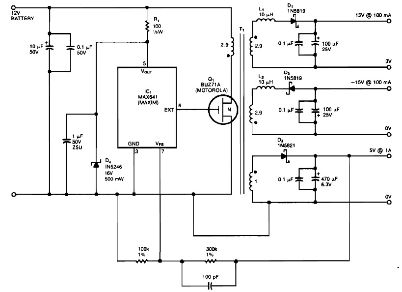
bipolar 15 v and 5v from car battery supply
Bipolar +/- 15V and 5V from car battery supply power supply. Refer to the specified page for an explanation of the related circuit diagram.
The described power supply circuit is designed to provide bipolar voltage outputs of +/- 15V and a...

Remote-Controlled Telephone/Fax Machine Switch
This system uses a transmitter operating at approximately 100 kHz to control a remote receiver. A line splitter can connect the transmitter to the active telephone line. The transmitter is a CMOS oscillator equipped with output buffer stages to drive...

Current spreading circuit diagram of a bipolar output
Current spreading bipolar output when the circuit diagram is as follows.
The circuit described involves a current spreading bipolar output configuration. This type of circuit is typically used in applications requiring efficient current distribution across multiple output paths, often seen in...

Bipolar power supply for battery instruments
To generate regulated ±5-V supplies from a pair of dry batteries, the circuit shown in Fig. 1 is commonly utilized. To protect against inadvertent reverse connection of a battery, a diode in series with each battery would create an unacceptable...

A BIPOLAR REGENERATIVE RECEIVER
Contrary to the beliefs of some radio experimenters, an efficient bipolar regenerative design is achievable. The primary concern lies in the low input impedance of the detector-amplifier bipolar stage. However, this can be effectively compensated for with positive feedback or...