


Rs-232C Line-Driven Cmos Circuits
#RS-232C
#CMOS
#MAX680
#line-driven
#serial communication
#voltage converter
#interface
#data transmission

Description: The circuit demonstrates a method for powering CMOS integrated circuits (ICs) using RS-232C lines. The MAX680 is typically employed to generate a voltage equal to ±2 Vcc. This circuit operates in the opposite manner, accepting ±10.5 to ±12V from the DTR and TD lines and outputting a 5.25 to 6 V signal. A pair of Schottky or silicon diodes rectifies each RS-232C line, and the resulting energy is stored in capacitors connected to the IC's V+ and V- pins. Capacitor C1, or both C1 and C2, then function as a reverse charge pump, transferring the stored energy from the V+ and V- pins to capacitor C3. The input source current for the MAX680 is approximately equal to the voltage drop across one of the diodes divided by the series resistance of 160 ohms. When powered by a 1488 driver with a ±12 V supply, this circuit can deliver 5 V at 3 mA. To increase the output current, multiple sets of diodes can be used on each RS-232 line, allowing for 5 V at 8 mA. The increased number of diodes results in lower source resistance, calculated as the inverse of the sum of the diodes' conductances. For applications requiring even higher output current, two MAX680s can be connected in parallel, with their V+ and V- capacitors tied together, while using separate C1 and C2 capacitors for each device. It is important to ensure that the power capability of the RS-232C lines is not exceeded when connecting devices in parallel.
The circuit is designed to efficiently convert the voltage levels from RS-232C communication lines into a usable power source for CMOS devices. The MAX680, a voltage regulator, plays a crucial role in this process by stabilizing the output voltage. The use of Schottky or silicon diodes is critical, as they provide low forward voltage drop, enhancing the efficiency of the rectification process.
The energy harvesting mechanism relies on the rectification of the RS-232C signal, which, when combined with the capacitive storage, allows for the generation of a stable output voltage. The capacitors connected to the V+ and V- pins are essential for smoothing out the rectified voltage and ensuring that the MAX680 operates within its specified parameters.
The reverse charge pumping action facilitated by capacitors C1 and C2 is a clever design choice, enabling the circuit to boost the voltage to the desired level. The relationship between the number of diodes used and the output current capacity is significant; as more diodes are added, the effective source resistance decreases, thereby allowing for greater current delivery without compromising the voltage stability.
In applications where higher current is needed, the parallel configuration of two MAX680 devices provides flexibility and scalability. Each device can independently manage its input capacitors, ensuring that variations in load do not adversely affect performance. Care must be taken to avoid exceeding the current ratings of the RS-232C lines, which could lead to signal integrity issues or potential damage to the communication interface.
This circuit is particularly useful in environments where CMOS devices require stable power supplies derived from existing communication lines, thus enhancing the versatility and functionality of RS-232C interfaces in electronic systems. The circuit illustrates a way to power CMOS ICs from RS-232C lines. The MAX680 is normally used to genera te a voltage equal to ±2 Vcc· This circuit does exactly the opposite. It takes in±10.5to±12V on the DTR and TD lines and puts out a 5.25- to 6-V signal. A pair of Schottky or silicon diodes rectifies each RS-232C line. The resultant energy is stored by the capacitors attached to the IC"s V + and V - pins. CI or both CI and C2 then reverse-charge pump the energy stored at the V + and V- pins to C3. The input source current of the MAX680 is approximately equal to the voltage drop of any one of the diodes that is divided by the series resistance of 160 . When you drive this circuit from a 1488 driver with a ± 12-V supply, it can deliver 5 V at 3 mA. To increase the output current, you can use as many as three sets of diodes on each RS-242 line to provide 5 V at 8 mA.
The more diodes you use, the lower the source resistance: Rs equals the inversion of the sum of the diodes" conductances. If your circuit requires even more output current, you can place two MAX680s in parallel, tie their V+ and V- capacitors together, and use separate CI and C2 capacitors for each ship.
If you do connect the devices in parallel, make sure not to exceed the power capability of the RS-232C lines.
The circuit is designed to efficiently convert the voltage levels from RS-232C communication lines into a usable power source for CMOS devices. The MAX680, a voltage regulator, plays a crucial role in this process by stabilizing the output voltage. The use of Schottky or silicon diodes is critical, as they provide low forward voltage drop, enhancing the efficiency of the rectification process.
The energy harvesting mechanism relies on the rectification of the RS-232C signal, which, when combined with the capacitive storage, allows for the generation of a stable output voltage. The capacitors connected to the V+ and V- pins are essential for smoothing out the rectified voltage and ensuring that the MAX680 operates within its specified parameters.
The reverse charge pumping action facilitated by capacitors C1 and C2 is a clever design choice, enabling the circuit to boost the voltage to the desired level. The relationship between the number of diodes used and the output current capacity is significant; as more diodes are added, the effective source resistance decreases, thereby allowing for greater current delivery without compromising the voltage stability.
In applications where higher current is needed, the parallel configuration of two MAX680 devices provides flexibility and scalability. Each device can independently manage its input capacitors, ensuring that variations in load do not adversely affect performance. Care must be taken to avoid exceeding the current ratings of the RS-232C lines, which could lead to signal integrity issues or potential damage to the communication interface.
This circuit is particularly useful in environments where CMOS devices require stable power supplies derived from existing communication lines, thus enhancing the versatility and functionality of RS-232C interfaces in electronic systems. The circuit illustrates a way to power CMOS ICs from RS-232C lines. The MAX680 is normally used to genera te a voltage equal to ±2 Vcc· This circuit does exactly the opposite. It takes in±10.5to±12V on the DTR and TD lines and puts out a 5.25- to 6-V signal. A pair of Schottky or silicon diodes rectifies each RS-232C line. The resultant energy is stored by the capacitors attached to the IC"s V + and V - pins. CI or both CI and C2 then reverse-charge pump the energy stored at the V + and V- pins to C3. The input source current of the MAX680 is approximately equal to the voltage drop of any one of the diodes that is divided by the series resistance of 160 . When you drive this circuit from a 1488 driver with a ± 12-V supply, it can deliver 5 V at 3 mA. To increase the output current, you can use as many as three sets of diodes on each RS-242 line to provide 5 V at 8 mA.
The more diodes you use, the lower the source resistance: Rs equals the inversion of the sum of the diodes" conductances. If your circuit requires even more output current, you can place two MAX680s in parallel, tie their V+ and V- capacitors together, and use separate CI and C2 capacitors for each ship.
If you do connect the devices in parallel, make sure not to exceed the power capability of the RS-232C lines.

Voltage Converter 3V to 5V using MAX660
Voltage converter circuit diagram for converting 3 volts to 5 volts using CMOS monolithic ICs MAX660 and MAX667, which functions as a positive voltage regulator.
The voltage converter circuit utilizes the MAX660 and MAX667 integrated circuits to step up a 3-volt...

Step down voltage converter 5v with transistor BC337
The circuit reduces voltage size or functions as a step-down voltage converter circuit, specifically a DC regulated circuit model using a switching converter. It generates the desired voltage output.
The step-down voltage converter circuit, also known as a buck converter, is...

Rs232c-led-circuit
Utilize a pair of Maxim's 5V-powered MAX231 RS-232C transmitters as drivers to achieve a dual-color LED. These transmitters necessitate only a single-ended, 5-V input to internally generate ±10 V. Their outputs are designed to be short-circuit-proof and can provide up...

VFC62 voltage / frequencyfrequency / voltage converter circuit
The VFC62 is a voltage-to-frequency and frequency-to-voltage converter that effectively transforms analog signals into digital signals. The digital output is presented in an open collector format, where the digital pulse repetition rate is directly proportional to the amplitude of the...

Repeating Interval Timer 2
This is a simpler repeating timer circuit. It uses just one CMOS IC wired as an asymmetric oscillator. The length of time the relay remains energized and the length of time it remains de-energized are set independently.
The repeating timer circuit...

1.5V liquid crystal display circuit
The Motorola company's MC14440 CMOS integrated circuit is designed for timing and displaying calendar functions. It utilizes a 32.768 kHz NT cutting type quartz crystal along with fine-tune capacitance to generate time-based signals. The display circuit operates on a 1.5...

Resonance generators by 4011 CMOS Gate
This resonance generator circuit, also known as an oscillating sound generator, is designed using the CMOS integrated circuit 4011 (Quad 2-Input NAND Gate). It consists of four NAND gates. Each oscillator circuit utilizes two gates. The circuit is capable of...

Cmos programmable divide-by-n counter
A single connection change allows division by any integer between 2 and 10. The RCA CD4017A Johnson decade counter is configured as a divide-by-7 counter. A resistor is utilized to maintain the reset line in a low state. When the...
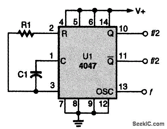
CD4047 CMOS OSCILLATOR
This CMOS square-wave oscillator utilizes the 4047 multivibrator circuit, suitable for both monostable (one-shot) and astable applications. In the provided configuration, the 4047 operates as an astable multivibrator. The circuit features three outputs from the 4047, with the first being...