


Frequency comparator circuit
#frequency comparator
#logic output
#shift register
#gating period
#IC
#digital circuit
#pulse initialization
#latching
#signal processing

Description: Input 1 functions as a gating period, during which a single rising edge on input 2 produces a logic 1 output. Any other input that indicates non-identical frequencies results in a logic 0 output. IC1a converts input 1 into a narrow pulse, which initializes IC2, a two-stage shift register that is clocked by input 2. Upon the first edge of input 2, a logic 1 is generated at the output of IC2b, while subsequent inputs yield a logic 0. At the conclusion of the gating period, this output is latched by IC3, resulting in the lock output. Additionally, since this is only valid for one input period, a monostable circuit is incorporated at the output to allow for visual monitoring. Depending on which state is deemed most critical, either output from IC3 can be utilized. The current configuration indicates a failure state.
The circuit utilizes a gating mechanism wherein Input 1 establishes a time window for valid signal detection from Input 2. The logic state of Input 2 is pivotal; a single rising edge during the gating period triggers a transition to a logic 1 output, while any other frequencies during this timeframe lead to a logic 0 output. This function is facilitated by IC1a, which processes Input 1 into a narrow pulse signal. This pulse serves as an initialization signal for IC2, which is configured as a two-stage shift register. The clocking of this shift register is directly influenced by Input 2. On the initial rising edge of Input 2, IC2b outputs a logic 1, indicating the detection of the valid signal, while all subsequent edges result in a logic 0 output, effectively creating a one-shot response to the first edge.
The output from IC2b is then latched by IC3 at the end of the gating period, establishing a lock output that signifies the successful capture of the input signal. To ensure that this output can be monitored visually, a monostable multivibrator is employed. This component generates a temporary pulse that can be observed, thus allowing for real-time monitoring of the system's state. The design allows for flexibility in output selection, enabling the user to choose between two outputs from IC3 based on the importance of the respective states. The current configuration is particularly useful for indicating a failure state, providing critical feedback for system diagnostics.Input 1 is used as a gating period, during which a single rising edge on input 2 will cause a logic 1 output-any other number, indicating non-identical frequencies causes a logic 0 output. ICla converts input 1 to a narrow pulse which initializes IC2 which forms a two-stage shift register clocked by input 2.
On the first edge of input 2 a logic 1 appears on the output of IC2b and for all subsequent inputs a logic 0 is present. At the end of the gating period this output is latched by IC3 forming the lock output. As this is only valid for one input period a monostable is added to the output to enable, for example, visual monitoring of the output. Either output from IC3 can be used depending on which state is most important. As connected the failure state is indicated.
The circuit utilizes a gating mechanism wherein Input 1 establishes a time window for valid signal detection from Input 2. The logic state of Input 2 is pivotal; a single rising edge during the gating period triggers a transition to a logic 1 output, while any other frequencies during this timeframe lead to a logic 0 output. This function is facilitated by IC1a, which processes Input 1 into a narrow pulse signal. This pulse serves as an initialization signal for IC2, which is configured as a two-stage shift register. The clocking of this shift register is directly influenced by Input 2. On the initial rising edge of Input 2, IC2b outputs a logic 1, indicating the detection of the valid signal, while all subsequent edges result in a logic 0 output, effectively creating a one-shot response to the first edge.
The output from IC2b is then latched by IC3 at the end of the gating period, establishing a lock output that signifies the successful capture of the input signal. To ensure that this output can be monitored visually, a monostable multivibrator is employed. This component generates a temporary pulse that can be observed, thus allowing for real-time monitoring of the system's state. The design allows for flexibility in output selection, enabling the user to choose between two outputs from IC3 based on the importance of the respective states. The current configuration is particularly useful for indicating a failure state, providing critical feedback for system diagnostics.Input 1 is used as a gating period, during which a single rising edge on input 2 will cause a logic 1 output-any other number, indicating non-identical frequencies causes a logic 0 output. ICla converts input 1 to a narrow pulse which initializes IC2 which forms a two-stage shift register clocked by input 2.
On the first edge of input 2 a logic 1 appears on the output of IC2b and for all subsequent inputs a logic 0 is present. At the end of the gating period this output is latched by IC3 forming the lock output. As this is only valid for one input period a monostable is added to the output to enable, for example, visual monitoring of the output. Either output from IC3 can be used depending on which state is most important. As connected the failure state is indicated.

Lights Out circuit
The design is based on the previous analysis of calculating the game in a circular shift register. While designing, it was realized that small extensions to the design would enable additional gameplay features, such as replay and manual input. The...

Frequency comparator II
The circuit provides a clear LED display indicating positive or negative values in increments of 0.1%. A reference frequency is generated by multiplying the input frequency using PLLIC1 and divider IC9, resulting in an output frequency of 64 times the...
Latching burglar alarm
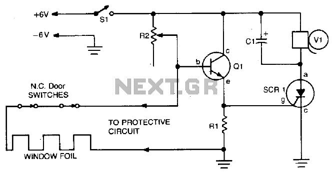
When the protective circuit is interrupted (opened), the alarm sounds. To set the circuit, adjust R2 (with the protective circuit open) for 1 V across R1.
The described circuit functions as a protective alarm system that activates when the integrity of...
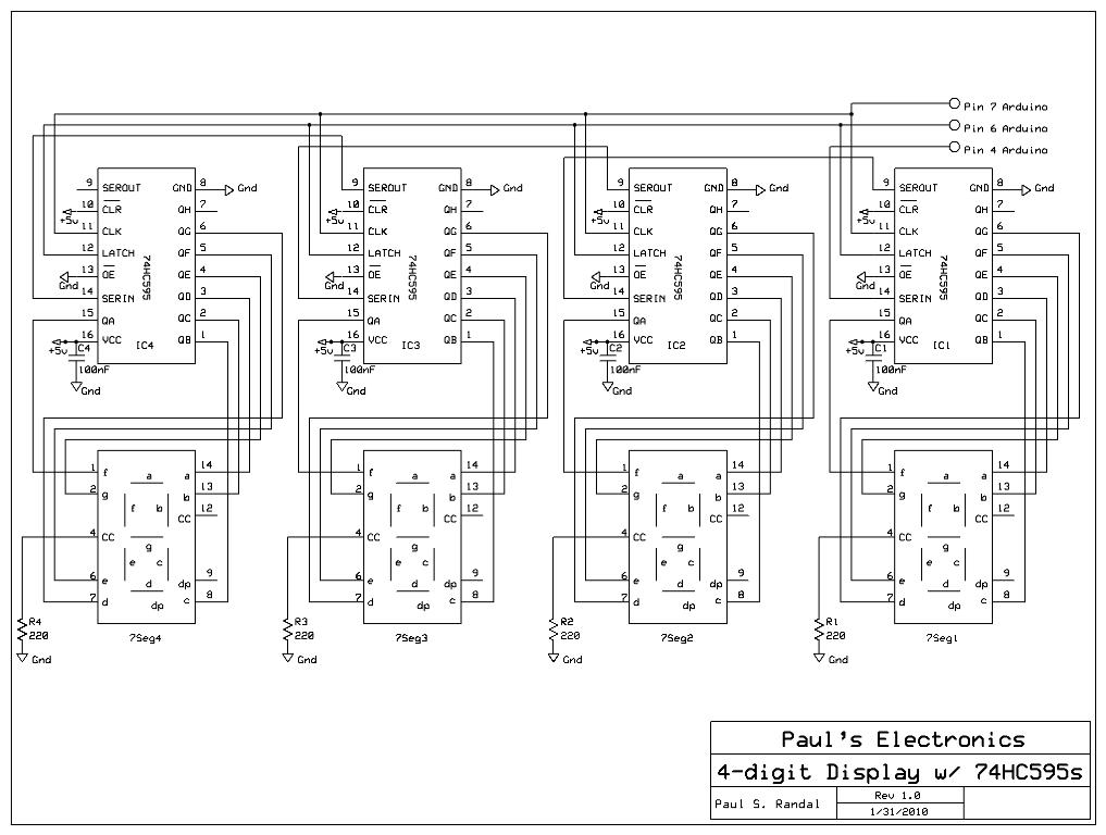
cascading shift registers to drive 7-segment displays with PC input
Four 595 shift registers are used together to drive 7-segment displays, with additional code implemented to accept input from a PC. Unlike the previous design that utilized 10-LED bar graphs, the current configuration employs 7-segment displays, which present a greater...

IC Voltage Regulators-withCircuit - Design & Theory
IC Voltage Regulators - Circuit diagram and block diagram of linear, fixed, adjustable (positive and negative), and switching voltage regulators.
IC voltage regulators are essential components in electronic circuits, providing stable output voltages from a varying input voltage source. They can...

2 Input Pulses Frequency Comparator
This circuit uses a 74HCT74, 74HCT00, and a LM311 to form a frequency comparator. The two pulse trains are fed to two D-type flip-flops (triggered by the leading edges). The flip-flops' outputs are compared in a NAND gate. If the...

Shift register on a schematic
The circuit features a shift register chip (74HC595N), which is not available on CircuitLab. There may be a specific representation for a shift register in schematic diagrams. Although assistance with CircuitLab is not provided, schematic illustrations can be referenced on...

Shift register driver
A 16V power supply can be synthesized using IN1692 rectifiers. A shift pulse input saturates the 2N2714, depriving the Darlington combination (2N2714 and 2N2868) of base drive. The negative pulse generated on the 15V line is differentiated to produce a...

Factory Alarm
The frequency is controlled by pin 5 of the integrated circuit (IC). When the power supply is activated, the capacitor charges gradually, which alters the voltage at pin 5 of the IC, causing the frequency to increase incrementally. Once the...