


Capacitive load drive circuit diagram of the MAX4106 4107
#MAX4106
#MAX4107
#capacitive load
#drive circuit
#isolation resistor
#AC characteristics
#operational amplifier

Description: The MAX4106/4107 is designed with a capacitive load drive circuit that includes an isolation resistor (Rs). While the MAX4106/4107 exhibits excellent AC characteristics, they are not optimized for driving high reactive loads. Utilizing a high reactive load may diminish the phase margin, resulting in pulse signal overshoot and ringing. To mitigate these issues, an isolation resistor (Rs) can be applied between the output terminal and the load. This resistor helps to suppress overshoot and oscillation, with a recommended resistance value ranging from 10 to 20 ohms. For the MAX4106, when RF is set to 120, the gain is 5V/V. In contrast, for the MAX4107, when RF is set to 270, the gain is 10V/V.
The MAX4106 and MAX4107 operational amplifiers are designed for high-speed applications, featuring a wide bandwidth and low distortion. The inclusion of an isolation resistor (Rs) is crucial when interfacing with capacitive loads, as these loads can introduce instability in the feedback loop, leading to undesirable oscillations. The isolation resistor serves to dampen these oscillations by introducing a controlled amount of resistance, which increases the phase margin and enhances stability.
When selecting the value for Rs, it is important to consider the specific application and the characteristics of the load. A resistor value between 10 and 20 ohms is generally effective for most applications, but fine-tuning may be necessary based on the load's reactance. The interaction between the isolation resistor and the capacitive load can significantly influence the performance of the amplifier.
The MAX4106 is optimized for a gain of 5V/V with a feedback resistor (RF) of 120 ohms, while the MAX4107 is configured for a gain of 10V/V with a feedback resistor of 270 ohms. These gain settings allow for flexibility in various applications, enabling the user to achieve the desired output level while maintaining signal integrity. Careful consideration of the feedback network design is essential to ensure optimal performance, as it directly affects the bandwidth and stability of the amplifier circuit.
In summary, the MAX4106/4107 operational amplifiers, when used with an appropriate isolation resistor and feedback network, can effectively drive capacitive loads while minimizing the risk of overshoot and ringing, thus ensuring reliable performance in high-speed electronic applications. As shown in FIG grounds MAX4106/4107 using a capacitive load drive circuit isolation resistor Rs constituted. MAX4106/4107 good AC characteristics, but they are not designed to drive high reactive load, such as using a high reactive load will reduce the phase margin, causing a pulse signal overshoot ringing and ringing. The circuit can eliminate the above problems may arise between the output terminal and the load applied isolation resistor Rs, can be used to suppress overshoot and ringing oscillation, Rs is resistance of 10 ~ 20.
When the chip MAX4106, and RF when 120, a gain of 5V/V; when the chip MAX4107, and RF to 270 at a gain of 10V/V.
The MAX4106 and MAX4107 operational amplifiers are designed for high-speed applications, featuring a wide bandwidth and low distortion. The inclusion of an isolation resistor (Rs) is crucial when interfacing with capacitive loads, as these loads can introduce instability in the feedback loop, leading to undesirable oscillations. The isolation resistor serves to dampen these oscillations by introducing a controlled amount of resistance, which increases the phase margin and enhances stability.
When selecting the value for Rs, it is important to consider the specific application and the characteristics of the load. A resistor value between 10 and 20 ohms is generally effective for most applications, but fine-tuning may be necessary based on the load's reactance. The interaction between the isolation resistor and the capacitive load can significantly influence the performance of the amplifier.
The MAX4106 is optimized for a gain of 5V/V with a feedback resistor (RF) of 120 ohms, while the MAX4107 is configured for a gain of 10V/V with a feedback resistor of 270 ohms. These gain settings allow for flexibility in various applications, enabling the user to achieve the desired output level while maintaining signal integrity. Careful consideration of the feedback network design is essential to ensure optimal performance, as it directly affects the bandwidth and stability of the amplifier circuit.
In summary, the MAX4106/4107 operational amplifiers, when used with an appropriate isolation resistor and feedback network, can effectively drive capacitive loads while minimizing the risk of overshoot and ringing, thus ensuring reliable performance in high-speed electronic applications. As shown in FIG grounds MAX4106/4107 using a capacitive load drive circuit isolation resistor Rs constituted. MAX4106/4107 good AC characteristics, but they are not designed to drive high reactive load, such as using a high reactive load will reduce the phase margin, causing a pulse signal overshoot ringing and ringing. The circuit can eliminate the above problems may arise between the output terminal and the load applied isolation resistor Rs, can be used to suppress overshoot and ringing oscillation, Rs is resistance of 10 ~ 20.
When the chip MAX4106, and RF when 120, a gain of 5V/V; when the chip MAX4107, and RF to 270 at a gain of 10V/V.
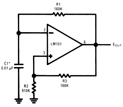
operational amplifier op amp oscillator
The timing capacitor (C1) generates multiple time constants, facilitating substantial voltage fluctuations at the input, attributable to the LM101's extensive input voltage range. It is advisable to decrease the value of resistor R2 and to increase the capacitance of C1...

Homemade whole integrated circuit amplifiers 01
The circuit depicted in Figure 5-60 and Figure 6 utilizes an operational amplifier (op-amp) configured as a channel pre-amplifier to address the signal loss introduced by the tone control circuit. Additionally, another group of op-amps forms a channel-driven stage amplifier...

Precision current sink sourcel
An operational amplifier circuit can provide a constant voltage source with a high amplification factor and substantial load current. Even with significant variations in circuit parameters, the output voltage maintains high precision. The output current limit is managed by transistors...

Operational Amplifier (Op-Amp) Oscillator
This is an operational amplifier (Op-Amp) oscillator circuit. This circuit has several advantages, including its ability to operate at low frequencies.
The operational amplifier oscillator circuit is designed to generate a periodic waveform output, typically a sine or square wave, using...
Precision current sink sourcel
An operational amplifier circuit can provide a constant voltage source with a high amplification factor and substantial load current. Even with significant variations in circuit parameters, the output voltage maintains high precision. The output current limit is managed by transistors...
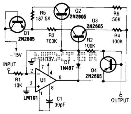
Nonlinear Operational Amplifier Circuit
This operational amplifier circuit utilizes resistor and transistor feedback elements to function as a nonlinear amplifier. The resistors R4 and R6 can be adjusted to modify the breakpoints as needed.
This operational amplifier circuit is designed to operate within the nonlinear...

Cosine wave Oscillator
This circuit is designed to output both a sine wave and a cosine wave. The design utilizes an operational amplifier, with the output frequency determined by component values set to 1Hz. The first operational amplifier generates a 1Hz sine wave,...

A delay circuit using an operational amplifier
A delay circuit utilizing an operational amplifier functions as a comparator, providing high timing accuracy. The timer's delay range is from 1 to 30 seconds. The delay time is determined by resistors Ri, RP, and capacitor C. By adjusting RP,...

cut the feed forward in the miller compensation with voltage buffer
An internally compensated operational amplifier has been fabricated using n-channel Al-gate MOS technology, utilizing only enhancement mode devices. The circuit is designed to ensure that its performance remains insensitive to process parameters. The input stage consists of a source-coupled differential...