


Capacitive load drive circuit diagram of the MAX4450 4451
#MAX4450
#MAX4451
#capacitive load
#drive circuit
#isolation resistor
#output terminals
#operational amplifier
#circuit diagram

Description: The circuit depicted in FIG demonstrates the MAX4450/4451 utilizing a capacitive load drive circuit with an isolation resistor (RISO). This configuration is situated between the output terminals and the load, along with an additional resistor, to mitigate overshoot and ringing oscillations. The resistance of RISO is specified to be between 20 and 30 ohms.
The MAX4450 and MAX4451 are high-speed operational amplifiers designed for applications requiring precise signal integrity and fast response times. In this context, the use of a capacitive load drive circuit is essential for ensuring stable operation when driving capacitive loads, which can introduce unwanted feedback and oscillations.
The isolation resistor (RISO) plays a critical role in this configuration by providing a damping effect. By placing RISO in series with the output, it helps to reduce the amplitude of any overshoot that may occur when the output transitions rapidly. This is particularly important in high-frequency applications where the risk of ringing oscillations can lead to signal distortion and potential damage to the output stage of the amplifier.
The specified resistance range of 20 to 30 ohms is optimal for balancing the trade-off between signal integrity and stability. A lower resistance may not sufficiently dampen the oscillations, while a higher resistance could degrade the signal quality and increase the output voltage drop. Therefore, careful selection of RISO is essential to maintain the performance characteristics of the MAX4450/4451 in applications where capacitive loads are present.
In summary, the integration of an isolation resistor in the capacitive load drive circuit for the MAX4450/4451 enhances the stability and reliability of the amplifier's performance by effectively managing overshoot and ringing, ensuring high fidelity in signal transmission. As shown in FIG grounds MAX4450/4451 using a capacitive load drive circuit isolation resistor RISO constructed. The circuit between the output terminals and the load plus a res istor RISO, for suppressing overshoot and ringing oscillation, RISO resistance is 20 ~ 30 .
The MAX4450 and MAX4451 are high-speed operational amplifiers designed for applications requiring precise signal integrity and fast response times. In this context, the use of a capacitive load drive circuit is essential for ensuring stable operation when driving capacitive loads, which can introduce unwanted feedback and oscillations.
The isolation resistor (RISO) plays a critical role in this configuration by providing a damping effect. By placing RISO in series with the output, it helps to reduce the amplitude of any overshoot that may occur when the output transitions rapidly. This is particularly important in high-frequency applications where the risk of ringing oscillations can lead to signal distortion and potential damage to the output stage of the amplifier.
The specified resistance range of 20 to 30 ohms is optimal for balancing the trade-off between signal integrity and stability. A lower resistance may not sufficiently dampen the oscillations, while a higher resistance could degrade the signal quality and increase the output voltage drop. Therefore, careful selection of RISO is essential to maintain the performance characteristics of the MAX4450/4451 in applications where capacitive loads are present.
In summary, the integration of an isolation resistor in the capacitive load drive circuit for the MAX4450/4451 enhances the stability and reliability of the amplifier's performance by effectively managing overshoot and ringing, ensuring high fidelity in signal transmission. As shown in FIG grounds MAX4450/4451 using a capacitive load drive circuit isolation resistor RISO constructed. The circuit between the output terminals and the load plus a res istor RISO, for suppressing overshoot and ringing oscillation, RISO resistance is 20 ~ 30 .

Unity gain line from the MAX4450 4451 a driving circuit diagram
The MAX4450/4451 unity gain line is illustrated in the driving circuit. The MAX4450/4451 features internal compensation, a 24-ohm resistor in series within a feedback loop, along with capacitors and inductors that can reduce the Q value of the feedback loop...

cut the feed forward in the miller compensation with voltage buffer
An internally compensated operational amplifier has been fabricated using n-channel Al-gate MOS technology, utilizing only enhancement mode devices. The circuit is designed to ensure that its performance remains insensitive to process parameters. The input stage consists of a source-coupled differential...

Long timed circuit diagram LM307N CA3094
The long timer circuit utilizes an operational amplifier, specifically the CA3094, to control the discharge formula for extended timing. This is typically achieved by adjusting the variable resistor RV1, which alters the timing duration to meet specific requirements.
The long timer...

Precision current sink sourcel
An operational amplifier circuit can provide a constant voltage source with a high amplification factor and substantial load current. Even with significant variations in circuit parameters, the output voltage maintains high precision. The output current limit is managed by transistors...

amplify voltage and build microphone circuit
An amplifier is a device that increases the voltage in a circuit. The simplest type is an operational amplifier, and this video will demonstrate how these devices function and how to implement them in electronic applications. As an example, you...
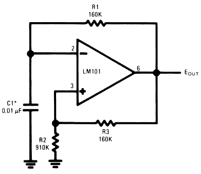
operational amplifier op amp oscillator
The timing capacitor (C1) generates multiple time constants, facilitating substantial voltage fluctuations at the input, attributable to the LM101's extensive input voltage range. It is advisable to decrease the value of resistor R2 and to increase the capacitance of C1...

A delay circuit using an operational amplifier
A delay circuit utilizing an operational amplifier functions as a comparator, providing high timing accuracy. The timer's delay range is from 1 to 30 seconds. The delay time is determined by resistors Ri, RP, and capacitor C. By adjusting RP,...
Precision current sink sourcel
An operational amplifier circuit can provide a constant voltage source with a high amplification factor and substantial load current. Even with significant variations in circuit parameters, the output voltage maintains high precision. The output current limit is managed by transistors...

Delay circuit of a multi-level output
A multi-stage delay circuit is presented in this schematic. The operational amplifiers are configured as comparators. Operational amplifier A1 operates when the voltage at the inverting input exceeds + VE. As the voltage at the inverting input of operational amplifiers...