


Sample-And-Hold Circuit I Circuit
#sample-and-hold
#op-amp
#analog
#signal processing
#capacitor
#switch
#hold mode
#sample mode
#voltage
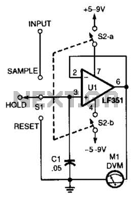
Description: This circuit demonstrates the principle of the sample-and-hold circuit. SI can be replaced by electronic switches (FET, etc.) in an actual application.
The sample-and-hold circuit is an essential component in various analog-to-digital conversion applications. Its primary function is to capture and hold a specific voltage level from an input signal for a predetermined period, allowing for accurate sampling of rapidly changing signals.
In a typical sample-and-hold circuit, the input signal is fed into a switch, which can be implemented using electronic devices such as Field Effect Transistors (FETs) or other suitable switching elements. When the switch is closed, the circuit samples the input voltage, and upon opening the switch, the sampled voltage is held constant at the output. This output can then be processed by an analog-to-digital converter (ADC) or any other subsequent circuitry.
The hold capacitor is a crucial component in this configuration, as it stores the sampled voltage. The choice of capacitance value is critical; it must be sufficiently large to maintain the voltage level without significant droop during the hold time. The circuit may also incorporate buffer amplifiers to prevent loading effects and ensure that the output impedance remains low, facilitating better interfacing with subsequent stages.
In practical applications, the switching mechanism can be designed to minimize charge injection and leakage currents, which are vital for maintaining the integrity of the sampled signal. The use of FETs as switches is advantageous due to their high input impedance and low power consumption, making them suitable for high-speed and low-noise applications.
Overall, the sample-and-hold circuit is a fundamental building block in modern electronic systems, enabling accurate signal processing in various fields, including telecommunications, instrumentation, and data acquisition systems. This circuit demonstrates the principle of the sample-and-hold circuit. SI can be replaced by electronic switches (FET, etc.) in an actual application.
The sample-and-hold circuit is an essential component in various analog-to-digital conversion applications. Its primary function is to capture and hold a specific voltage level from an input signal for a predetermined period, allowing for accurate sampling of rapidly changing signals.
In a typical sample-and-hold circuit, the input signal is fed into a switch, which can be implemented using electronic devices such as Field Effect Transistors (FETs) or other suitable switching elements. When the switch is closed, the circuit samples the input voltage, and upon opening the switch, the sampled voltage is held constant at the output. This output can then be processed by an analog-to-digital converter (ADC) or any other subsequent circuitry.
The hold capacitor is a crucial component in this configuration, as it stores the sampled voltage. The choice of capacitance value is critical; it must be sufficiently large to maintain the voltage level without significant droop during the hold time. The circuit may also incorporate buffer amplifiers to prevent loading effects and ensure that the output impedance remains low, facilitating better interfacing with subsequent stages.
In practical applications, the switching mechanism can be designed to minimize charge injection and leakage currents, which are vital for maintaining the integrity of the sampled signal. The use of FETs as switches is advantageous due to their high input impedance and low power consumption, making them suitable for high-speed and low-noise applications.
Overall, the sample-and-hold circuit is a fundamental building block in modern electronic systems, enabling accurate signal processing in various fields, including telecommunications, instrumentation, and data acquisition systems. This circuit demonstrates the principle of the sample-and-hold circuit. SI can be replaced by electronic switches (FET, etc.) in an actual application.

Circuit examples
Input J4 features an offset function that is activated only when no plug is inserted into J4, as the switching contact of J4 connects to the positive supply voltage through the protection resistor R8. The inverting sum of all inputs...

Norton-amplifier
The non-inverting amplifier has a gain of R2/R3 (1 in this case) and produces a voltage of V during a positive excursion of Vin with respect to ground. The inverting amplifier accommodates the negative excursions of V; its gain is...

Simulator Test Tools Speed Circuit Design
A zero-crossing detector converts an input sine wave (Vin) into a square wave, which, when high, charges an op-amp integrator. A reference-input square wave subsequently discharges the integrator. The output voltage of the integrator at the end of this charge/discharge...

Absolute value amplifier
The circuit generates a positive output voltage for either polarity of input. For positive signals, it functions as a non-inverting amplifier, while for negative signals, it operates as an inverting amplifier. The accuracy is poor for input voltages under 1V;...

ELF MONITOR
The capacitor instrument is not intended for measuring the capacitance of capacitors; rather, it is designed to identify whether a capacitor is functional or defective, as well as to detect short circuits or open circuits. This functionality provides reliable quality...
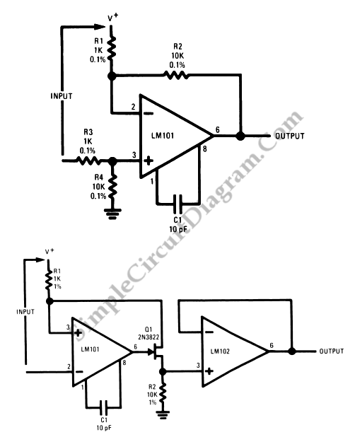
Op-Amp Application: Level Shifting Amplifier
In linear equipment design, it is sometimes necessary to take a voltage that is referenced to a certain DC level and generate an amplified output that is also referenced.
In linear circuit design, the process of amplifying a voltage that is...

Automatic mooring light
The integrated circuit U1, which can be an LF351 or a 741 operational amplifier, functions as a comparator to regulate lighting. Resistors R2 and R3 establish a reference voltage of approximately 2.5 volts at pin 3 of U1. When light...
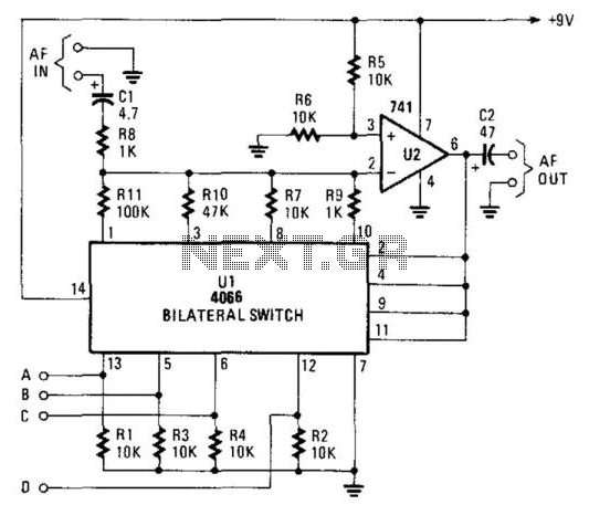
Gain-Controlled Op Amp
The gain controller utilizes a 4066 quad bilateral switch to electronically select a feedback resistor for the 741 operational amplifier. One or more switches can be activated simultaneously to achieve a stepped, variable-gain range from less than 1 to 100.
The...

op amp IR Demodulator Design
Designing an infrared (IR) demodulator circuit to replace the one shown in this question. The goal is to demodulate a simple IR signal modulated at 32.678 kHz, with the requirement of detecting the presence of the signal without packet decoding....