


Frequency Shift Keyer
#frequency shift keyer
#differential amplifier
#gate voltage
#rf signal
#modulation
#communication
#signal processing

Description: Apply a signal to each differential amplifier input pair. When the gate voltage changes from one extreme to the other, the output can alternate between the two input signals. When the gate level is high (1.5 V), a signal applied between pins 5 and 6 (channel A) will be transmitted, while a signal applied between pins 3 and 4 (channel B) will be suppressed. This process results in a binary-to-frequency conversion that is directly related to the binary sequence driving the gate input (pin 2).
The described circuit utilizes a differential amplifier configuration to achieve signal selection based on the gate voltage level. In this configuration, the differential amplifier has two input channels: channel A and channel B, associated with pins 5, 6 and pins 3, 4, respectively. The operation of the circuit is contingent upon the voltage level present at the gate input (pin 2).
When the gate voltage is set to a high level of 1.5 V, the circuit is designed to allow the signal from channel A (pins 5 and 6) to pass through while simultaneously suppressing the signal from channel B (pins 3 and 4). This selective signal processing enables the circuit to effectively switch between two input signals based on the gate voltage, facilitating the conversion of a binary input into a frequency output.
The binary-to-frequency conversion is directly influenced by the binary sequence applied to the gate input. As the binary sequence changes, the gate voltage transitions between its high and low states, causing the circuit to alternate the output signal between the two channels. This results in a frequency output that corresponds to the binary input sequence, making the circuit suitable for applications in digital signal processing, communication systems, and data encoding.
In summary, the described differential amplifier circuit provides a means to convert binary signals into frequency outputs through controlled signal selection based on gate voltage levels, enhancing its utility in various electronic applications. Apply a signal to each differential amplifier input pair. When the gate voltage is changed from one extreme to the ot her, the output can be switched alternately between the two input signals. When the gate level is high (1.5 V), a signal applied between pins 5 and 6 (channel A) will be passed and a signal applied between pins 3 and 4 (channel B) will be suppressed. In this manner, a binary-to-frequency conversion is obtained that is directly related to the binary sequence, which is driving the gate input (pin 2).
The described circuit utilizes a differential amplifier configuration to achieve signal selection based on the gate voltage level. In this configuration, the differential amplifier has two input channels: channel A and channel B, associated with pins 5, 6 and pins 3, 4, respectively. The operation of the circuit is contingent upon the voltage level present at the gate input (pin 2).
When the gate voltage is set to a high level of 1.5 V, the circuit is designed to allow the signal from channel A (pins 5 and 6) to pass through while simultaneously suppressing the signal from channel B (pins 3 and 4). This selective signal processing enables the circuit to effectively switch between two input signals based on the gate voltage, facilitating the conversion of a binary input into a frequency output.
The binary-to-frequency conversion is directly influenced by the binary sequence applied to the gate input. As the binary sequence changes, the gate voltage transitions between its high and low states, causing the circuit to alternate the output signal between the two channels. This results in a frequency output that corresponds to the binary input sequence, making the circuit suitable for applications in digital signal processing, communication systems, and data encoding.
In summary, the described differential amplifier circuit provides a means to convert binary signals into frequency outputs through controlled signal selection based on gate voltage levels, enhancing its utility in various electronic applications. Apply a signal to each differential amplifier input pair. When the gate voltage is changed from one extreme to the ot her, the output can be switched alternately between the two input signals. When the gate level is high (1.5 V), a signal applied between pins 5 and 6 (channel A) will be passed and a signal applied between pins 3 and 4 (channel B) will be suppressed. In this manner, a binary-to-frequency conversion is obtained that is directly related to the binary sequence, which is driving the gate input (pin 2).

Simple differential amplifier circuit
Operational amplifiers A1 and A2 are connected in a non-inverting configuration to form amplifier A3. The operational amplifier A3 can be classified as a subtractor circuit that converts the differential signal between the floating points X and Y into a...

Double-Sideband Suppressed-Carrier (DSB-SC) Modulator
When a carrier signal is modulated using amplitude modulation, four frequency components are produced. The first component is the modulating signal itself, the second is the carrier frequency, while the last two are the sum and difference of the carrier...

Differential amplifier circuit four connection methods and compare the characteristics of a
A differential amplifier circuit can be configured in four different connection methods, allowing for a comparison of characteristics such as gain and common-mode rejection ratio (CMRR). This analysis focuses on symmetrical circuits and their performance in handling common-mode signals.
The differential...
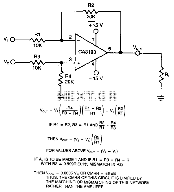
Differential-amplifier
This differential amplifier utilizes a CA3193 BiMOS operational amplifier. It serves as a classical differential input-to-signal-ended output converter, which, when paired with a low-resistance signal source, will sustain a high common-mode rejection ratio (CMRR), provided that R1 equals R3 plus...

Having a differential amplifier and overcurrent protection for power supply circuit 2
The circuit features a current protection mechanism utilizing transistors VTa, VT4, and a sense resistor Ro. When an overcurrent or short-circuit fault occurs, the power supply cannot resume normal operation because the conduction condition of VT3 remains unchanged, resulting in...

modulation
A reason to modulate a message signal is to match the communication channel's frequency. This is necessary because the information to be sent over the channel is often at a relatively low frequency. For instance, the frequency range of music...

Diamond differential amplifier circuit input
Almost all DC amplifier circuits are utilized as the input stage of differential circuits. Many complementary symmetry circuits also employ a double differential complementary sub-circuit along with a constant current source for the input stage. The constant current source possesses...

Modulation-monitor
Switching diodes are utilized to activate the neon lamps when negative-peak modulation reaches 50%, 60%, and 100%. To operate the circuit effectively, it is important to monitor the lamps. The 50% lamp should ideally be firing continuously, the 60% lamp...

Variable gain differential amplifier circuit diagram A709
The configuration of the variable gain A709 differential amplifier circuit is illustrated. The primary advantage of this circuit is its ability to maintain a constant common-mode rejection ratio (CMRR) while allowing for continuous adjustments to the differential gain. The circuit...