Frequency Response Analysis of Amplifiers
1. Definition and Importance of Frequency Response
1.1 Definition and Importance of Frequency Response
The frequency response of an amplifier describes how its gain and phase shift vary with the frequency of the input signal. Mathematically, it is represented by the transfer function H(f), which is a complex-valued function of frequency f. The magnitude of H(f) gives the gain, while the argument provides the phase shift:
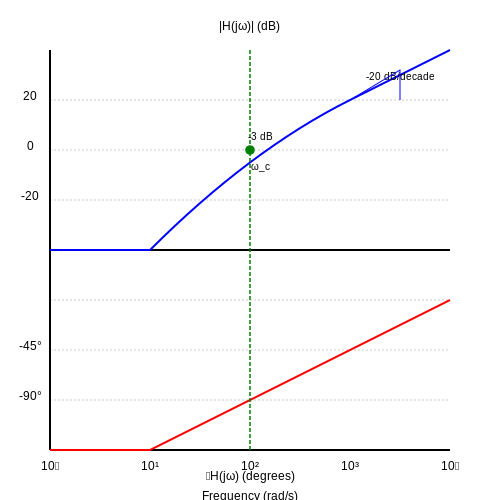
where |H(f)| is the magnitude response and ϕ(f) is the phase response. The frequency response is typically plotted as a Bode plot, which consists of two separate graphs: one for magnitude (in decibels) and another for phase (in degrees), both plotted against a logarithmic frequency scale.
Bandwidth and Cutoff Frequencies
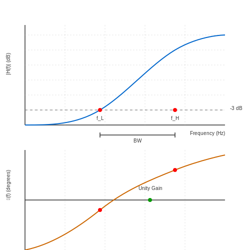
The bandwidth of an amplifier is defined as the range of frequencies over which the gain remains within 3 dB of its maximum value. The lower and upper cutoff frequencies, fL and fH, mark the points where the gain drops to 1/√2 (≈ 0.707) of its midband value. For a single-pole amplifier, the bandwidth BW is given by:
In many practical amplifiers, fL is negligible compared to fH, simplifying the bandwidth to BW ≈ fH.
Importance in Practical Applications
Understanding frequency response is critical in designing amplifiers for specific applications. For instance:
- Audio Amplifiers: Must maintain a flat frequency response across the audible range (20 Hz to 20 kHz) to avoid distortion.
- RF Amplifiers: Need precise bandwidth control to avoid interference with adjacent channels.
- Operational Amplifiers: Require stability analysis to prevent oscillations due to phase shifts near the unity-gain frequency.
Frequency-Domain Limitations
Amplifiers exhibit deviations from ideal behavior due to parasitic capacitances, inductances, and semiconductor physics. For example, the Miller effect introduces an effective capacitance that reduces high-frequency gain. Similarly, coupling and bypass capacitors introduce low-frequency poles, affecting fL.
The dominant pole approximation simplifies analysis by assuming one pole dominates the frequency response. For an amplifier with poles at f1, f2, ..., fn, the upper cutoff frequency is approximated as:
This approximation is particularly useful in multistage amplifiers where multiple poles interact.
Real-World Case Study: Op-amp Frequency Compensation
In operational amplifiers, frequency compensation is used to ensure stability. A dominant pole is intentionally introduced (e.g., via a compensation capacitor) to roll off the gain before secondary poles cause excessive phase shift. The gain-bandwidth product (GBW) remains constant:
where AOL is the open-loop gain. This principle is fundamental in feedback amplifier design.
1.2 Key Parameters: Bandwidth, Cutoff Frequencies, and Gain
Bandwidth and Its Significance
The bandwidth (BW) of an amplifier defines the range of frequencies over which it operates effectively, bounded by the lower and upper cutoff frequencies (fL and fH). Mathematically, it is expressed as:
For amplifiers where fL is negligible (e.g., DC-coupled amplifiers), the bandwidth simplifies to fH. The bandwidth determines the amplifier's ability to faithfully reproduce input signals without distortion. In audio applications, for instance, a wider bandwidth ensures accurate reproduction of high-frequency components.
Cutoff Frequencies and the -3 dB Point
The cutoff frequencies fL and fH correspond to the frequencies at which the amplifier's gain drops to 1/√2 (≈ 0.707) of its midband value, equivalent to a -3 dB reduction in gain. These points mark the boundaries of the amplifier's usable frequency range.
The lower cutoff frequency fL is primarily governed by coupling and bypass capacitors, which act as high-pass filters. The upper cutoff frequency fH is limited by parasitic capacitances and the transistor's inherent frequency response, forming a low-pass filter.
Gain-Bandwidth Product (GBW)
The gain-bandwidth product is a critical figure of merit for amplifiers, particularly in operational amplifiers. It defines the trade-off between gain and bandwidth:
For a given amplifier, increasing the voltage gain Av reduces the bandwidth proportionally, keeping the GBW constant. This relationship is crucial in high-frequency design, where achieving both high gain and wide bandwidth is challenging.
Frequency Response and Bode Plots
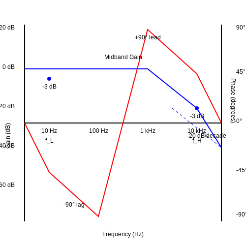
The frequency response of an amplifier is often visualized using Bode plots, which depict gain (in dB) and phase shift as functions of frequency. A typical Bode magnitude plot shows:
- A flat midband region with constant gain
- A -20 dB/decade roll-off below fL due to high-pass characteristics
- A -20 dB/decade roll-off above fH due to low-pass characteristics
The phase response shows a 90° lag at low frequencies and a 90° lead at high frequencies, with the total phase shift through the amplifier being the sum of these effects.
Practical Considerations in Amplifier Design
In real-world applications, several factors influence these key parameters:
- Parasitic capacitances: Junction capacitances (Cπ, Cμ in BJTs) reduce fH
- Miller effect: Amplifies the effective input capacitance in inverting amplifiers
- Temperature: Affects transistor parameters and thus frequency response
- Loading effects: Subsequent stages may reduce overall bandwidth
Advanced techniques like cascode configurations or negative feedback are often employed to extend bandwidth while maintaining gain stability.
1.3 Decibels (dB) and Bode Plots
Definition and Mathematical Basis of Decibels
The decibel (dB) is a logarithmic unit used to express ratios of power, voltage, or current in electronic systems. For power ratios, the decibel is defined as:
where P1 and P2 are the input and output power levels, respectively. For voltage or current ratios, the definition adjusts to account for the square-law relationship between power and voltage/current in resistive systems:
This logarithmic scaling compresses wide dynamic ranges into manageable numbers, making it indispensable in amplifier frequency response analysis.
Bode Plots: Representation of Frequency Response
A Bode plot is a graphical representation of a system's frequency response, consisting of two components:
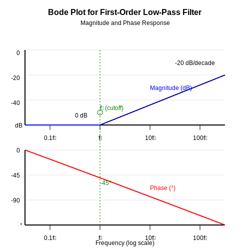
- Magnitude Plot – Displays the gain (in dB) versus frequency on a logarithmic scale.
- Phase Plot – Shows the phase shift (in degrees) versus frequency.
The magnitude response of an amplifier is typically approximated using piecewise linear asymptotes. For a first-order low-pass filter with a cutoff frequency fc, the gain rolls off at -20 dB/decade beyond fc:
Practical Applications and Interpretation
Bode plots are essential in stability analysis, particularly in feedback amplifier design. The gain margin and phase margin are derived from Bode plots to assess stability:
- Gain Margin – The amount of additional gain required to make the system unstable (measured at the frequency where phase shift reaches -180°).
- Phase Margin – The additional phase shift needed to induce instability (measured at the frequency where gain crosses 0 dB).
For example, an amplifier with a phase margin below 45° may exhibit undesirable ringing or oscillations.
Higher-Order Systems and Break Frequency Analysis
Second-order systems introduce additional complexity due to resonant peaks and steeper roll-off rates. The quality factor (Q) determines the sharpness of the peak near the resonant frequency f0:
In Bode plots, a high Q results in a pronounced peak at f0, while a low Q leads to a more gradual transition.
Case Study: Operational Amplifier Frequency Compensation
Frequency compensation techniques, such as dominant-pole compensation, modify the open-loop gain of an op-amp to ensure stability. The compensated Bode plot shows a single-pole roll-off until the unity-gain frequency, preventing phase shifts from exceeding critical thresholds.
2. Low-Frequency Response of Common-Emitter Amplifiers
Low-Frequency Response of Common-Emitter Amplifiers
The low-frequency response of a common-emitter (CE) amplifier is primarily governed by the coupling and bypass capacitors, which introduce high-pass filtering effects. At low frequencies, the impedance of these capacitors becomes significant, leading to signal attenuation and phase shifts. To analyze this behavior rigorously, we examine the amplifier’s small-signal equivalent circuit and derive the transfer function.
Dominant Poles and Break Frequencies
The low-frequency cutoff (fL) is determined by the RC time constants associated with the input coupling capacitor (C1), output coupling capacitor (C2), and emitter bypass capacitor (CE). Each capacitor contributes a pole to the transfer function:
where Rin is the input resistance seen at the base, and REeq is the equivalent resistance seen by CE, given by:
Input and Output Coupling Effects
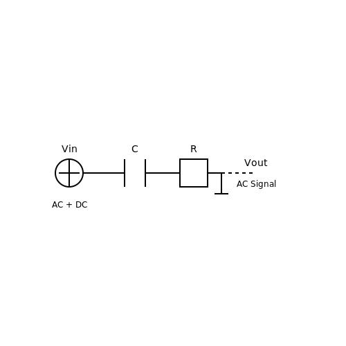
The input coupling capacitor C1 forms a high-pass filter with the Thévenin equivalent resistance of the source and base circuitry. For frequencies below fC1, the signal is attenuated at −20 dB/decade. Similarly, C2 interacts with the load and collector resistances, introducing another high-pass pole.
Emitter Bypass Capacitor Impact
The bypass capacitor CE is critical for maintaining voltage gain at mid-band frequencies. At low frequencies, its impedance rises, reducing the effective transconductance and introducing a pole at fCE. This pole often dominates the low-frequency response due to the smaller equivalent resistance REeq.
Composite Frequency Response
The overall low-frequency response is the superposition of the individual poles. If one pole is significantly lower than the others (e.g., fCE ≪ fC1, fC2), it becomes the dominant cutoff frequency. The total phase shift at fL approaches +90° due to the cascaded high-pass filters.
Design Considerations
To minimize low-frequency distortion:
- Choose CE such that fCE is at least a decade below the lowest operating frequency.
- Ensure C1 and C2 are large enough to avoid attenuating the signal band.
- In audio applications, typical values for CE range from 10–100 µF, while C1 and C2 may be 1–10 µF.
Practical Measurement and SPICE Simulation
In lab settings, a Bode plotter or network analyzer can measure the amplitude and phase response. SPICE simulations (e.g., using LTspice) model these effects by including parasitic capacitances and non-ideal capacitor ESR. For accurate results, the transistor’s small-signal parameters (e.g., rπ, β) must be extracted from the DC operating point.
2.2 High-Frequency Response of Common-Source Amplifiers
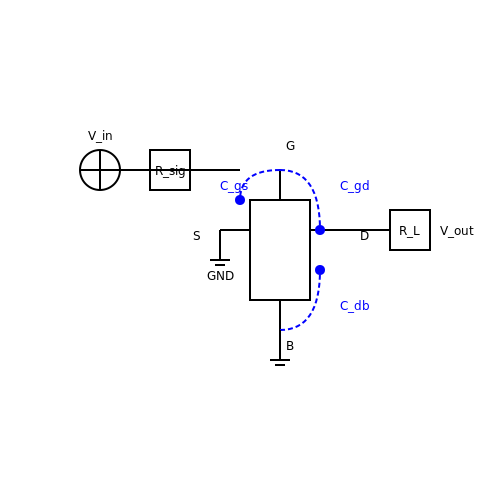
The high-frequency response of a common-source (CS) amplifier is primarily governed by the parasitic capacitances inherent in the MOSFET and the circuit layout. These capacitances form low-pass networks that attenuate the signal as frequency increases. The dominant capacitances include the gate-to-drain capacitance (Cgd), gate-to-source capacitance (Cgs), and drain-to-bulk capacitance (Cdb).
Small-Signal Model and High-Frequency Limitations
At high frequencies, the small-signal model of a CS amplifier must account for the MOSFET's intrinsic capacitances. The simplified high-frequency equivalent circuit includes:
- Cgs — Gate-to-source capacitance, which affects the input time constant.
- Cgd — Gate-to-drain capacitance (Miller capacitance), which introduces feedback and reduces bandwidth.
- Cdb — Drain-to-bulk capacitance, contributing to the output pole.
The total input capacitance (Cin) is influenced by the Miller effect, where Cgd appears multiplied by the amplifier's gain (Av) at the input:
Similarly, the output capacitance (Cout) includes the Miller component of Cgd and the drain-bulk capacitance:
Bandwidth and Dominant Pole Approximation
The bandwidth of a CS amplifier is determined by the poles associated with the input and output nodes. The input pole (fin) and output pole (fout) are given by:
where Rsig is the source resistance and RL is the load resistance. The dominant pole, typically the lower of the two, dictates the amplifier's −3 dB bandwidth.
Impact of the Miller Effect
The Miller effect significantly degrades high-frequency performance by increasing the effective input capacitance. This effect is particularly pronounced in high-gain amplifiers, where Cgd is multiplied by the voltage gain. To mitigate this, designers employ techniques such as:
- Cascode topologies — Reduce the Miller effect by minimizing the voltage swing across Cgd.
- Inductive peaking — Extends bandwidth by introducing resonance at high frequencies.
Frequency Response and Bode Plot Analysis
The transfer function of a CS amplifier in the high-frequency domain can be approximated as a two-pole system:
where Av0 is the mid-band gain, and ωp1 and ωp2 are the pole frequencies. A Bode plot of the response typically shows a roll-off at −20 dB/decade after the first pole and −40 dB/decade after the second.
Practical Considerations in Design
In real-world applications, the high-frequency response is also affected by layout parasitics, such as interconnect capacitance and inductance. Advanced fabrication processes with smaller feature sizes reduce intrinsic capacitances, enabling wider bandwidths. However, trade-offs between gain, bandwidth, and power dissipation must be carefully balanced.
Frequency Response of Operational Amplifiers
Open-Loop Gain and Bandwidth
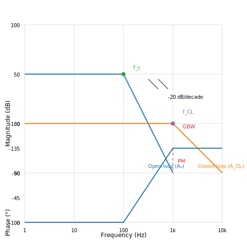
The open-loop gain (AOL) of an operational amplifier (op-amp) is frequency-dependent, characterized by a dominant pole that causes a roll-off at -20 dB/decade. The gain-bandwidth product (GBW) defines the frequency at which the open-loop gain drops to unity (0 dB). For a single-pole response:
where A0 is the DC gain, f is the frequency, and fc is the corner frequency. The GBW is given by:
Closed-Loop Frequency Response
When negative feedback is applied, the closed-loop gain (ACL) modifies the frequency response. For a non-inverting amplifier with feedback factor β:
At frequencies well below the closed-loop bandwidth, AOL(f)β ≫ 1, simplifying to:
The closed-loop bandwidth (fCL) is determined by the GBW and closed-loop gain:
Slew Rate and Large-Signal Behavior
At high frequencies, the op-amp's slew rate (SR) limits the maximum rate of output voltage change. For a sinusoidal input V(t) = V_p \sin(2πft), the maximum frequency before slew-induced distortion is:
This effect becomes critical in high-speed applications where large output swings are required.
Stability and Phase Margin
Negative feedback systems must maintain stability, quantified by the phase margin (PM). A PM > 45° is typically desired. The PM is derived from the open-loop transfer function:
where fu is the frequency where |AOL(fu)β| = 1. Compensation techniques (e.g., Miller compensation) are often employed to ensure adequate PM.
Practical Considerations
Real op-amps exhibit additional poles and zeros beyond the dominant pole, affecting high-frequency performance. For instance, the Texas Instruments OPA1612 has a GBW of 40 MHz and a slew rate of 20 V/μs, making it suitable for audio applications where low distortion is critical.
Parasitic capacitances in PCB layouts can introduce unintended poles, degrading phase margin. Careful grounding and minimization of trace lengths are essential for preserving high-frequency response.
3. Small-Signal Models for Frequency Analysis
Small-Signal Models for Frequency Analysis
Hybrid-π Model for BJTs
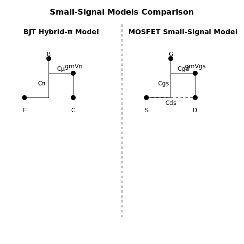
The hybrid-π model is a small-signal representation of a bipolar junction transistor (BJT) that captures frequency-dependent behavior. At high frequencies, parasitic capacitances between terminals dominate the response. The model includes:
- Transconductance (gm): Relates base-emitter voltage to collector current.
- Base-emitter capacitance (Cπ): Combines diffusion and junction capacitances.
- Base-collector capacitance (Cμ): Represents the reverse-biased junction capacitance.
where IC is the DC collector current, VT the thermal voltage, Cje the emitter junction capacitance, and τF the forward transit time.
MOSFET Small-Signal Model
The MOSFET small-signal model for frequency analysis includes intrinsic capacitances and channel resistance:
- Gate-source capacitance (Cgs): Dominates at high frequencies.
- Gate-drain capacitance (Cgd): Causes Miller effect in amplifiers.
- Drain-source capacitance (Cds): Shunts output at RF frequencies.
where W and L are device dimensions, Cox the oxide capacitance, and Cov overlap capacitance.
High-Frequency Limitations
The transition frequency fT marks where current gain drops to unity. For BJTs:
For MOSFETs, the figure of merit depends on gate charging time:
In RF amplifiers, fT must exceed the operating frequency by 5-10× for acceptable gain.
Miller Effect in Amplifiers
The Miller effect multiplies Cgd in common-source amplifiers by the voltage gain Av:
This creates a dominant pole that limits bandwidth. Cascode topologies mitigate this by isolating Cgd from the input.
SPICE Model Parameters
For accurate simulation, SPICE models require:
- BJT: TF (forward transit time), CJC (base-collector capacitance), VAF (Early voltage).
- MOSFET: CGSO, CGDO (overlap capacitances), CBD (bulk-drain capacitance).
3.2 Miller Effect and Its Impact on Bandwidth
Fundamentals of the Miller Effect
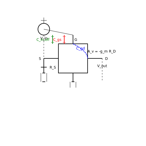
The Miller effect arises due to the interaction between the input and output of an amplifier through a feedback capacitance, typically the parasitic capacitance Cgd (gate-drain capacitance in FETs) or Cμ (collector-base capacitance in BJTs). When a voltage gain stage has a gain Av, the effective input capacitance increases significantly due to this feedback mechanism.
Here, Cgs is the intrinsic gate-source capacitance, and Cgd is the gate-drain capacitance. The term Cgd(1 + |Av|) represents the Miller-multiplied capacitance, which dominates the input impedance at high frequencies.
Mathematical Derivation of Bandwidth Limitation
The bandwidth of an amplifier is inversely proportional to the total input capacitance and the source resistance Rs. The upper cutoff frequency (fH) is determined by the time constant formed by Rs and Cin,eff:
Substituting Cin,eff from the earlier equation:
This shows that as the gain |Av| increases, the bandwidth fH decreases proportionally. The product of gain and bandwidth (GBW) remains constant for a given amplifier topology, illustrating the fundamental trade-off imposed by the Miller effect.
Practical Implications in Amplifier Design
The Miller effect is particularly problematic in high-gain stages, such as common-emitter (BJT) or common-source (FET) amplifiers. To mitigate its impact, designers employ techniques such as:
- Cascode topologies – By adding a common-base/gate stage, the voltage gain across Cgd is reduced, minimizing the Miller multiplication.
- Neutralization – Introducing a compensating capacitor to cancel the effect of Cgd.
- Shunt peaking – Using inductive elements to extend bandwidth beyond the RC-limited cutoff.
Case Study: Miller Effect in Operational Amplifiers
In op-amps, the Miller effect is deliberately exploited in compensation networks (e.g., Miller capacitors) to stabilize the amplifier by introducing dominant-pole compensation. The capacitor CC across a high-gain stage ensures stability but at the cost of reduced bandwidth:
where Rout is the output resistance of the gain stage. This principle is widely used in frequency compensation of multi-stage amplifiers.
3.3 Dominant Pole Approximation
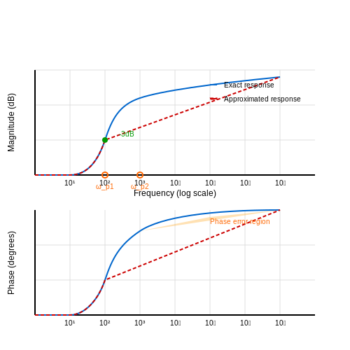
The dominant pole approximation simplifies the analysis of multi-pole systems by assuming that one pole dominates the frequency response. This is particularly useful in amplifier design, where higher-order poles often exist but their impact is negligible compared to the lowest-frequency (dominant) pole.
Mathematical Basis
Consider a transfer function with multiple poles:
If one pole frequency ωp1 is significantly lower than all others (ωp1 ≪ ωp2, ωp3, ..., ωpn), the transfer function can be approximated as:
This approximation holds when ω ≪ ωp2, where the contributions of higher poles are negligible.
Validity Conditions
The dominant pole approximation is valid when:
- The ratio between the second-lowest pole and dominant pole satisfies ωp2/ωp1 ≥ 5
- The frequency range of interest is below the second pole (ω < ωp2)
- Zeros (if present) are at frequencies much higher than ωp1
Practical Applications
In amplifier design, the dominant pole approximation is used to:
- Simplify stability analysis in feedback systems
- Estimate bandwidth without solving higher-order equations
- Design compensation networks by intentionally creating a dominant pole
Error Analysis
The error introduced by neglecting non-dominant poles can be quantified by comparing the exact and approximate phase margins. For a two-pole system, the phase error at ω = ωp1 is:
When ωp2 = 5ωp1, this error is approximately 11.3°, which is often acceptable for initial designs.
Design Example
Consider an operational amplifier with poles at:
The dominant pole approximation holds for frequencies below 1MHz, yielding a simplified transfer function:
This approximation accurately predicts the -3dB bandwidth while greatly simplifying calculations of gain and phase response in the audio frequency range.
4. Experimental Methods: Sweep Generators and Network Analyzers
4.1 Experimental Methods: Sweep Generators and Network Analyzers
Sweep Generators: Principles and Operation
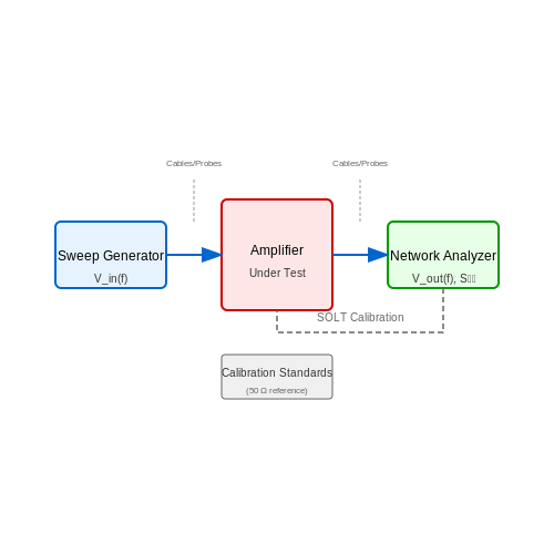
Sweep generators are essential for characterizing the frequency response of amplifiers by providing a continuous, time-varying sinusoidal signal whose frequency spans a defined range. The output voltage Vout(f) of an amplifier under test is measured as the input frequency f is swept, typically in logarithmic steps to cover wide bandwidths efficiently. Modern sweep generators employ direct digital synthesis (DDS) for precise frequency control, with phase-locked loops (PLLs) ensuring stability.
where Av(f) is the voltage gain as a function of frequency. Nonlinearities in the sweep generator’s output must be minimized, as harmonic distortion can corrupt measurements. Calibration against a known reference (e.g., a 50 Ω termination) is necessary to account for source impedance mismatches.
Network Analyzers: Scalar vs. Vector Measurements
Network analyzers provide comprehensive frequency-domain characterization by measuring both magnitude and phase response. Scalar network analyzers (SNAs) capture only amplitude (e.g., |S21|), while vector network analyzers (VNAs) extract complex S-parameters, enabling impedance and group delay analysis. A VNA’s error-correction algorithms (e.g., SOLT calibration) compensate for systematic imperfections in cables, connectors, and fixtures.
Here, a1 and b2 represent incident and reflected wave amplitudes, respectively. The analyzer’s receiver must maintain linearity across its dynamic range to avoid compression artifacts, particularly when testing high-gain amplifiers.
Practical Considerations and Calibration
Key experimental challenges include:
- Noise floor limitations: Low-level signals require averaging or narrow intermediate bandwidth (IF) settings to improve SNR.
- Impedance matching: Mismatches at the amplifier’s input/output ports introduce ripple errors, mitigated by using attenuators or tuners.
- Temperature drift: Active components in the test setup may exhibit gain variations, necessitating periodic recalibration.
For high-frequency measurements (>1 GHz), waveguide or microprobe fixtures replace coaxial connections to minimize parasitic inductance/capacitance. Time-domain gating (in VNAs) can isolate the amplifier’s response from spurious reflections in long test cables.
Case Study: Measuring a 1–10 GHz Low-Noise Amplifier
A typical procedure involves:
- Performing a full 2-port calibration up to the probe tips using a CS-5 impedance standard substrate.
- Setting the sweep generator to output −30 dBm to avoid amplifier compression.
- Capturing S21 with 10 kHz IF bandwidth and 16 averages to resolve the amplifier’s 2 dB gain flatness specification.
De-embedding techniques subtract the fixture’s insertion loss from raw data, revealing the true device performance. Advanced analyzers support nonlinear measurements (e.g., 1 dB compression point) by superimposing a power sweep on the frequency sweep.
4.2 SPICE Simulation for Frequency Response Analysis
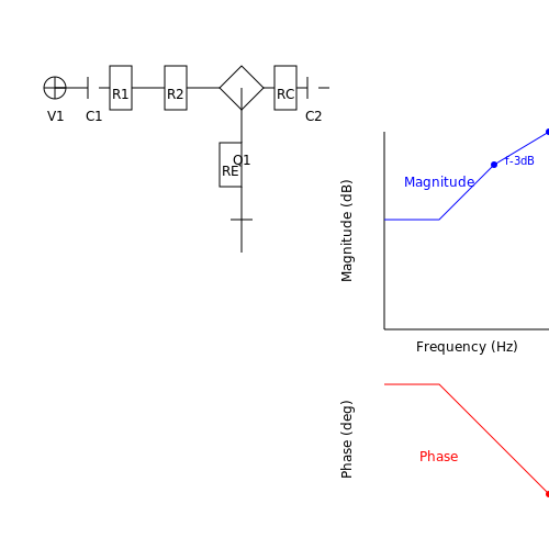
SPICE (Simulation Program with Integrated Circuit Emphasis) is an industry-standard tool for analyzing the frequency response of amplifiers. Unlike analytical methods, SPICE simulations account for non-ideal component behavior, parasitic effects, and nonlinearities, making them indispensable for high-fidelity design validation.
Setting Up the AC Analysis
To perform frequency response analysis, SPICE uses an AC small-signal analysis sweep. The simulation linearly or logarithmically varies the input frequency while measuring the output voltage or current. The key parameters are:
- Start Frequency (Fstart): Typically 1 Hz or lower for audio amplifiers.
- Stop Frequency (Fstop): Must exceed the amplifier’s expected bandwidth by at least a decade.
- Points per Decade: A minimum of 100 ensures smooth Bode plots.
Netlist Configuration
A minimal SPICE netlist for a common-emitter amplifier includes:
* Common-Emitter Amplifier AC Analysis
V1 in 0 AC 1
R1 in base 10k
R2 base 0 2.2k
RC collector VCC 1k
RE emitter 0 220
C1 base emitter 10u
C2 collector out 10u
RL out 0 10k
Q1 collector base emitter NPN
.model NPN NPN(Is=1e-16 Bf=100)
.ac dec 100 1 100Meg
.end
Interpreting Simulation Results
SPICE generates:
- Magnitude Plot: Gain (dB) vs. frequency, revealing bandwidth (f-3dB) and roll-off.
- Phase Plot: Phase shift (degrees) vs. frequency, critical for stability analysis.
The gain-bandwidth product (GBW) is derived from the unity-gain frequency (fT):
Advanced Techniques
For multi-stage amplifiers, pole-zero analysis identifies dominant poles and zeros:
.pz V(out) V1Monte Carlo analysis assesses robustness by varying component tolerances:
.mc 1000 ac V(out) LIST R1(R) R2(R) RC(R) RE(R)Practical Considerations
Real-world SPICE models must include:
- Parasitic capacitances (Cbe, Cbc) in transistor models.
- PCB trace inductances for RF designs.
- Temperature effects via
.tempsweeps.
4.3 Interpreting Simulation Results
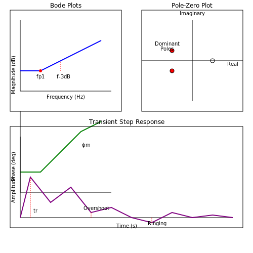
When analyzing amplifier frequency response through simulation, the primary outputs consist of Bode plots (magnitude and phase), pole-zero diagrams, and transient response characteristics. Each provides distinct insights into the amplifier's behavior across frequency.
Bode Plot Interpretation
The magnitude plot reveals three critical regions:
- Low-frequency rolloff - Shows effects of coupling capacitors and DC blocking elements
- Midband gain - The stable gain region where the amplifier operates as intended
- High-frequency rolloff - Demonstrates the limits imposed by parasitic capacitances and device bandwidth
The phase plot complements this by showing the phase margin at unity gain, crucial for stability analysis. A phase shift approaching -180° at the gain crossover frequency indicates potential oscillation.
Pole-Zero Analysis
Pole-zero plots provide direct visualization of the system dynamics. The dominant pole frequency fp1 typically sets the -3dB point:
where Ceq represents the equivalent capacitance at the dominant node. Non-dominant poles above the unity-gain frequency can significantly impact stability.
Transient Response Correlation
Step response simulations should correlate with frequency domain results. The rise time tr relates to bandwidth by:
Overshoot in the transient response indicates inadequate phase margin, typically below 45°. Ringing corresponds to complex conjugate poles with low damping factors.
Impedance Profile Analysis
Network analyzer simulations reveal impedance mismatches that may not appear in simple AC analysis. The reflection coefficient Γ shows matching quality:
Impedance peaks at resonant frequencies indicate potential stability issues or unwanted feedback paths.
Noise Figure Interpretation
Noise simulations should be evaluated in context of the Friis cascade formula:
Where Fn represents the noise factor of each stage and Gn the available gain. The noise figure (NF = 10log10F) typically increases at both low and high frequencies due to 1/f noise and reduced gain respectively.
Distortion Products
Harmonic distortion simulations reveal nonlinear behavior. The third-order intercept point (IP3) can be extracted from two-tone simulations:
where ΔP is the difference between fundamental and third-order product power levels. Compression point (P1dB) typically occurs 10-12dB below IP3.
5. Compensation Techniques for Improved Bandwidth
5.1 Compensation Techniques for Improved Bandwidth
Dominant Pole Compensation
Dominant pole compensation introduces a low-frequency pole to shape the amplifier's open-loop response, ensuring stability while extending the usable bandwidth. The transfer function of a compensated amplifier can be expressed as:
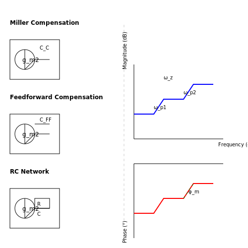
where ωp1 is the dominant pole and ωp2 is the secondary pole. By positioning ωp1 sufficiently low, the phase margin is improved, preventing oscillations. This technique is commonly implemented using a Miller capacitor (CC) across high-gain stages, which creates the dominant pole through the effective multiplication of capacitance by the stage's gain.
Lead Compensation
Lead compensation introduces a zero in the transfer function to counteract phase lag from existing poles. The compensated transfer function becomes:
The zero (ωz) is placed near the second pole (ωp2), effectively canceling its phase contribution. This is achieved in practice by adding a resistor in series with the Miller capacitor, creating an RC network that introduces the zero without significantly affecting the dominant pole.
Feedforward Compensation
Feedforward techniques bypass high-impedance nodes to provide a high-frequency signal path, improving bandwidth without compromising stability. In a two-stage amplifier, a feedforward capacitor (CFF) connects the input of the first stage to the output of the second stage, creating a parallel signal path for high frequencies. The effective bandwidth enhancement can be derived as:
where gm2 is the transconductance of the second stage, CL is the load capacitance, and CC is the Miller compensation capacitor.
Active Feedback Compensation
Active feedback networks use additional transistors to create controlled feedback paths that stabilize the amplifier. In a three-stage design, an intermediate stage can be used to sense and correct phase shifts before they accumulate. The stability condition for such systems is given by:
where ωu is the unity-gain frequency and φm is the phase margin. Active compensation provides better control over pole-zero placement compared to passive techniques.
Practical Implementation Considerations
When implementing compensation techniques, several non-ideal effects must be considered:
- Parasitic capacitances can introduce unintended poles above the unity-gain frequency
- Process variations affect the exact placement of poles and zeros
- Power consumption increases with more complex compensation networks
- Noise performance may degrade due to additional components in the signal path
Modern operational amplifiers often combine multiple compensation techniques. For example, the Ahuja compensation scheme uses both Miller compensation and feedforward paths to achieve bandwidths exceeding 100 MHz with phase margins above 60°.
5.2 Stability Analysis and Phase Margin
The stability of an amplifier is determined by its frequency response, particularly the behavior of its loop gain at the frequency where the magnitude falls to unity (0 dB). If the phase shift at this frequency approaches -180°, the feedback becomes positive, potentially leading to oscillations. The phase margin quantifies how far the system is from instability.
Defining Phase Margin
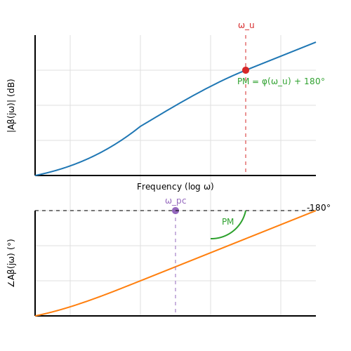
Phase margin (PM) is the difference between the actual phase shift and -180° at the frequency where the loop gain magnitude is unity (0 dB):
where:
- ωu (unity-gain frequency) is where |Aβ(jω)| = 1 (0 dB),
- φ(ωu) is the phase shift at ωu.
A phase margin of 45° or higher is typically required for stable operation. Lower values lead to excessive ringing and overshoot, while negative phase margin results in instability.
Bode Plot Analysis
Stability is most commonly assessed using Bode plots of the loop gain Aβ(jω). Two critical frequencies are:
- Gain crossover frequency (ωgc): Where |Aβ(jω)| = 1 (0 dB).
- Phase crossover frequency (ωpc): Where ∠Aβ(jω) = -180°.
If ωgc < ωpc, the system is stable. The phase margin is evaluated at ωgc, while the gain margin is the reciprocal of |Aβ(jω)| at ωpc.
Pole-Zero Effects on Stability
Each pole contributes -90° phase shift at high frequencies, while zeros add +90°. A two-pole system has a maximum phase shift of -180°, but with sufficient separation between poles, the phase margin remains acceptable. Additional poles degrade stability:
where ωp2 and ωp3 are the second and third pole frequencies.
Compensation Techniques
To improve phase margin:
- Dominant-pole compensation: Introduce a low-frequency pole to roll off gain before higher poles contribute phase lag.
- Miller compensation: Use capacitor feedback to split poles, increasing separation.
- Lead compensation: Add a zero to counteract phase lag near ωgc.
Practical Considerations
In real-world amplifiers, parasitic capacitances and inductances introduce additional poles. SPICE simulations or network analyzers are often used to measure phase margin experimentally. For multi-stage amplifiers, nested feedback loops must be analyzed separately to ensure global stability.
5.3 Trade-offs Between Gain and Bandwidth
The relationship between gain and bandwidth in amplifiers is fundamentally governed by the gain-bandwidth product (GBW), a key figure of merit in amplifier design. For a single-pole amplifier, the GBW remains constant, implying that increasing the gain reduces the bandwidth proportionally, and vice versa. This trade-off arises from the intrinsic limitations of active devices and feedback networks.
Mathematical Derivation of Gain-Bandwidth Product
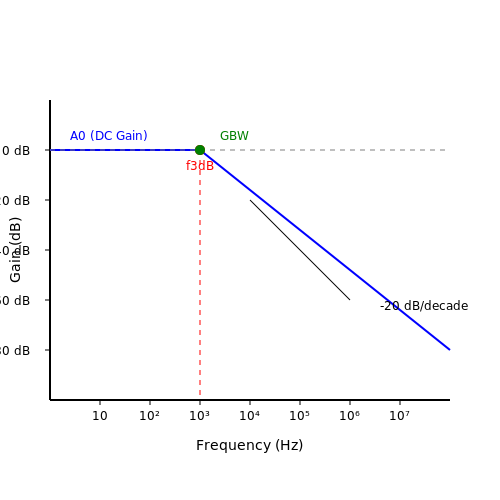
Consider an amplifier with a single dominant pole at frequency fp. The frequency-dependent voltage gain A(f) can be expressed as:
where A0 is the DC gain. The magnitude of the gain at frequency f is:
The 3-dB bandwidth (f3dB) occurs when |A(f)| = A0/√2, yielding:
The gain-bandwidth product is then defined as:
For multi-stage amplifiers, the GBW concept extends, but interactions between poles complicate the relationship, often requiring compensation techniques to maintain stability.
Practical Implications in Amplifier Design
In real-world applications, the gain-bandwidth trade-off imposes critical constraints:
- High-Gain Amplifiers exhibit reduced bandwidth, limiting their use in high-frequency applications unless gain stages are carefully optimized.
- Broadband Amplifiers must sacrifice gain to achieve wider frequency response, often necessitating cascaded stages or feedback topologies.
- Operational Amplifiers leverage internal compensation to fix the GBW, ensuring stability at the cost of flexible gain adjustments.
Case Study: Op-Amp Frequency Compensation
A dominant-pole compensation capacitor is often used in op-amps to enforce a single-pole response, stabilizing the amplifier while setting a predictable GBW. For example, the LM741 op-amp has a typical GBW of 1 MHz, meaning:
- At a gain of 100, the bandwidth is approximately 10 kHz.
- At unity gain, the bandwidth extends to 1 MHz.
This behavior is critical in feedback systems, where phase margin and stability depend on the controlled roll-off of gain with frequency.
Advanced Techniques to Mitigate Trade-offs
Several methods exist to partially decouple gain and bandwidth limitations:
- Cherry-Hooper Topology: Uses local feedback to enhance bandwidth without severely degrading gain.
- Distributed Amplification: Employs transmission lines to combine gain stages, achieving multi-octave bandwidths.
- Noise-Shaping Techniques: Allows selective gain enhancement in specific frequency bands.
These approaches are essential in RF and microwave amplifiers, where both high gain and wide bandwidth are often required simultaneously.
6. Recommended Textbooks on Amplifier Design
6.1 Recommended Textbooks on Amplifier Design
- Electronic Circuit Analysis[Book] - O'Reilly Media — Electronic Circuit Analysis is designed to serve as a textbook for a two semester undergraduate course on electronic circuit analysis. ... 6.13 Emitter Follower Transistor Amplifier Analysis; 6.14 Frequency Response of RC-Coupled CE Transistor Amplifier ... 13.14 Radio Frequency Amplifiers (Tuned Amplifier) 13.15 Wideband Amplifiers; 13.16 ...
- PDF Department of Electrical Engineering and Computer Science Massachusetts ... — ˜ frequency response, gain-bandwidth product 14.3 to 14.3.2 ˜ output voltage swing, saturation p 1007 ˜ output current limit 14.1.1, p 956: short ckt protection ˜ compensation 12.10.3 on p 919 ˜ slew rate 14.3.3 ˜ offset voltage and drift 14.4 to 14.4.2; 14.6.1 ˜ op-amp selection considerations 9. Operational Amplifiers ˜ non-linear op ...
- PDF SCHUBERT, JR. • KIM Series Editor: Fundamentals of Electronics: Book 3 ... — Active Filters and Amplifier Frequency Response, and the first two books in the series, Electronic Devices and Circuit Applications (ISBN 9781627055628), and Amplifiers: Analysis and Design (ISBN 9781627055642), form an appropriate body of material for such a course. Series ISSN: 1932-3166 About SYNTHESIS
- PDF 1.6 Frequency Response of Amplifiers - TONG IN OH — 1.6.1 Amplifier Frequency Response •Whenever a sinewave signal is applied to a linear circuit, the resulting output is sinusoidal with the same frequency as the input •Transfer function / amplifier transmission •Magnitude of the amplifier gain @ 𝜔: 𝑻(𝝎)=𝑉𝑜 𝑉𝑖 •Phase of the amplifier transmission: ∠𝑇𝜔=𝜙
- PDF CHAPTER 3 Frequency Response of Basic BJT and MOSFET Amplifiers — Electronic amplifiers are limited in frequency response in that the response magnitude falls off from a constant mid-band value to lower values both at frequencies below and above an intermediate range (the mid-band) of frequencies. A typical frequency response curve of an amplifier system appears as in figure3.3.
- PDF CHAPTER 3 Frequency response Amp v2 - Concordia University — A typical frequency response curve of an amplifier system appears as in figure3.3. Figure 3.3: Typical frequency response function magnitude plot for an electronic amplifier Using the concepts of Bode magnitude plot technique, we can approximate the low-frequency portion of the sketch above by an expression of the form s a Ks TL s r o (, ) a s K
- Semiconductor Devices: Theory and Application - Open Textbook Library — 6.4 Frequency Response and Noise; 6.5 Miller's Theorem; Summary; Chapter 7: BJT Small Signal Amplifiers. 7.0 Chapter Objectives; 7.1 Introduction; 7.2 Simplified AC Model of the BJT; 7.3 Common Emitter Amplifier; 7.4 Common Collector Amplifier; 7.5 Common Base Amplifier; 7.6 Multi-Stage Amplifiers; Summary; Chapter 8: BJT Class A Power ...
- PDF Fundamentals of Electronic Circuit Design - University of Cambridge — 8 Operational Amplifiers 8.1 Op amp Basics 8.2 Op amp circuits 8.2.1 non-inverting amplifier 8.2.2 inverting amplifier 8.2.3 signal offset 9 Filters 9.1 The Decibel Scale 9.2 Single-pole Passive Filters 9.3 Metrics for Filter Design 9.4 Two-pole Passive Filters 9.5 Active Filters 9.5.1 First order low pass 9.5.2 First order high pass
- High-Frequency Circuit Design and Measurements — An elective course in the final-year BEng progamme in electronic engin eering in the City Polytechnic of Hong Kong was generated in response to the growing need of local industry for graduate engineers capable of designing circuits and performing measurements at high frequencies up to a few gigahertz. ... 6 Small-signal Amplifier Design -- 6. ...
- Frequency Response of Transistor Amplifiers | SpringerLink — 6.1.3 Emitter Bypass Capacitor. The most effective biasing scheme used with the common emitter amplifier is the voltage divider biasing shown in Fig. 6.9.This circuit includes an input coupling capacitor C i, an output coupling capacitor C o, and a bypass capacitor C E.The low-frequency effects of C i and C o have already been determined. In order to determine the effect of C E, C i, and C o ...
6.2 Key Research Papers on Frequency Response Analysis
- PDF frequency response - edw.PDF — The system frequency response contains not just information of the system's response at a particular frequency, but can contain information at all frequencies of interest. Since a system's frequency response involves find the sinusoidal steady-state response of a system, the techniques can be considered to be applications of phasor analysis.
- PDF 1.6 Frequency Response of Amplifiers - TONG IN OH — 1.6.3 Evaluating the Frequency Response Analytically obtaining an expression for the frequency response To evaluate the frequency response of an amplifier, Inductance L: • Capacitance C: Frequency domain analysis (impedance and/or admittance) ( ) • Amplifier transfer function ( ) = ( ) Using complex frequency variable, s, Inductance L:
- PDF Microsoft Word - CHAPTER 3_Frequency response _Amp_v2 — Electronic amplifiers are limited in frequency response in that the response magnitude falls off from a constant mid-band value to lower values both at frequencies below and above an intermediate range (the mid-band) of frequencies. A typical frequency response curve of an amplifier system appears as in figure3.3.
- Transistor Amplifier Frequency Response | SpringerLink — Generally, the frequency response analysis of a transistor amplifier system is shown by plotting its gain that is the size of its output signal to its input signal. The frequency response of a given frequency-dependent circuit can be displayed as a graphical sketch of magnitude (gain) against frequency (ƒ).
- Frequency Response of Transistor Amplifiers | SpringerLink — While the analysis is done using the JFET, it also applies in general to the MOSFET. After completing this chapter, the reader will be able to: Determine the low-frequency response of transistor amplifiers Determine the high-frequency response of transistor amplifiers
- Frequency Response of Transistor Amplifiers | SpringerLink — While the analysis is done using the JFET, it applies in general to the MOSFET also. After completing the chapter, the reader will be able to Determine the low-frequency response of transistor amplifiers Determine the high-frequency response of transistor amplifiers
- PDF 6.012.FT00.Lecture.21.1.ppt - MIT — Summary of Key f T(short -circuit -gain current -off cut frequency ) figure of merit to assess response of transistors In MOSFET, to first order Tf = pt T where tTis transit the of electrons time the channel In common -source amplifier, voltage frequency Cgsand because Cgdshort circuit the
- Transistor Frequency-Response Analysis: Recursive Shunt-Circuit ... — This paper proposes an insightful design-based frequency response analysis of transistor circuits that also serves as the reference analysis for all single-stage amplifier primitives.
- PDF Lecture 13: Frequency Response — Lecture 13: Frequency Response Mark Hasegawa-Johnson ECE 401: Signal and Image Analysis, Fall 2021 ... When we process a signal, usually, we're trying to enhance the meaningful part, and reduce the noise. Spectrum helps us to understand which part is meaningful, and which part is noise.
- PDF A High Bandwidth, Low Distortion, Fully Differential Ampli — this amplifier has a strong influence on its frequency response. Thus, the out-put impedance can be used to adju t the bandwidth and amount of peaking in the frequency response. The overall system requir
6.3 Online Resources and Tutorials
- PDF CHAPTER 3 Frequency Response of Basic BJT and MOSFET Amplifiers — Electronic amplifiers are limited in frequency response in that the response magnitude falls off from a constant mid-band value to lower values both at frequencies below and above an intermediate range (the mid-band) of frequencies. A typical frequency response curve of an amplifier system appears as in figure3.3.
- PDF Design of Analog Integrated Circuits - 國立臺灣大學 — Chap. 5 Frequency Response of Amplifiers Textbook Chapter 6 6.1 General Considerations 6.2 Common-Source Stage 6.3 Source Followers 6.4 Common-Gate Stage 6.5 Cascode Stage 6.6 Differential Pair 6.7 Gain-Bandwidth Trade-Offs ... Direct Analysis •"Dominant pole" approximation.
- PDF CHAPTER 3 Frequency response Amp v2 - Concordia University — A typical frequency response curve of an amplifier system appears as in figure3.3. Figure 3.3: Typical frequency response function magnitude plot for an electronic amplifier Using the concepts of Bode magnitude plot technique, we can approximate the low-frequency portion of the sketch above by an expression of the form s a Ks TL s r o (, ) a s K
- PDF Frequency Response Analysis - ahmed.ucoz.org — displaying the frequency response is to plot the magnitude and phase of G(j!) versus !. These plots for the example above are shown in Figure 6.2. Figure 6.2: Frequency response. 6.2 Bode diagrams This section presents a method for plotting a frequency response that is di erent from the two methods given in the rst section of this chapter. This
- PDF ECE 342 Electronic Circuits Lecture 26 Response of Cascaded Amplifiers — Frequency Response of Cascaded Amplifiers. ECE 342 -Jose Schutt‐Aine 2 CE Cascade Amplifier Exact analysis too tedious ... Cascode Amplifier - High Frequency. Title: Microsoft PowerPoint - Lec_26 Author: joseschutt Created Date: 7/20/2018 8:05:07 AM ...
- PDF SECTION 7: FREQUENCY- RESPONSE ANALYSIS - Oregon State University ... — Frequency Response Peaking For systems with 𝜁𝜁< 0.707, the gain response will exhibit peaking Can relate peak magnitude to the damping ratio 𝑀𝑀 𝑝𝑝 = 1 2𝜁𝜁1−𝜁𝜁 2 Relative to low-frequency gain And the peak frequency to the damping ratio and natural frequency 𝜔𝜔 𝑝𝑝 = 𝜔𝜔 𝑛𝑛 1−2𝜁𝜁 2
- PDF 1.6 Frequency Response of Amplifiers - TONG IN OH — 1.6.1 Amplifier Frequency Response •Whenever a sinewave signal is applied to a linear circuit, the resulting output is sinusoidal with the same frequency as the input •Transfer function / amplifier transmission •Magnitude of the amplifier gain @ 𝜔: 𝑻(𝝎)=𝑉𝑜 𝑉𝑖 •Phase of the amplifier transmission: ∠𝑇𝜔=𝜙
- 6.4: Frequency Response and Noise - Engineering LibreTexts — In contrast, a radio frequency amplifier may be operating at frequencies orders of magnitude higher than these. Without exception, all amplifiers have an upper limit frequency, \(f_2\), but not all of them have a lower frequency limit, \(f_1\). Amplifiers without a lower limit can amplify signals with frequencies all the way down to DC.
- Resources | Signals and Systems - MIT OpenCourseWare — Learning Resource Types. theaters Lecture Videos. assignment_turned_in Problem Sets with Solutions. grading Exams with Solutions. menu_book Online Textbook. ... Frequency Response and Bode Plot Lecture 11: Continuous-time frequency response and Bode plots Lecture 12: Continuous-Time (CT) Feedback and Control, Part 1 Lecture 12: Continuous-time ...
- Purdue University ECE 255 : Introduction To Electronic Analysis And ... — chapter 1: 1.1 Signal, 1.2 Frequency spectrum of signals, 1.3 Analog and digital signals, 1.4.1 Signal amplification, 1.4.2 Aplifier circuit symbol, 1.4.3 Voltage gain, 1.4.4 Power gain and current gain, 1.4.5 Gain in DB, 1.4.6 Amplifier power supply, 1.4.7 Amplifier saturation, 1.4.8 Symbol convention