Phase Locked Loops
1. Basic Concept and Working Principle
1.1 Basic Concept and Working Principle
Fundamental Operation
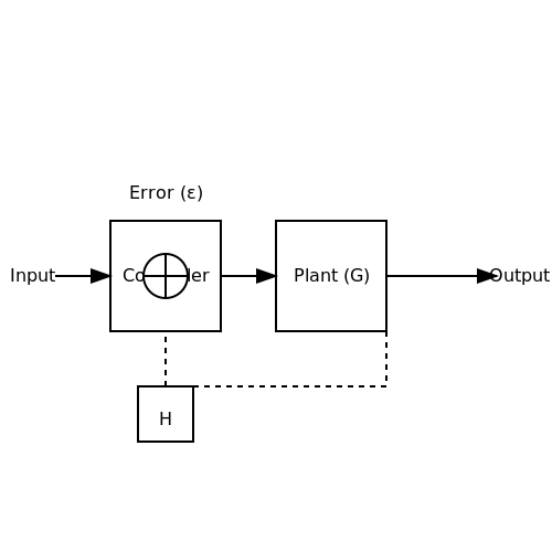
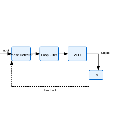
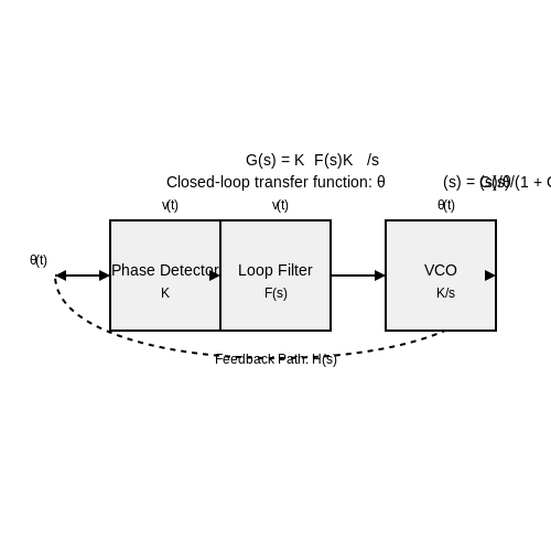
A phase-locked loop (PLL) is a feedback control system that synchronizes the phase and frequency of an output signal with a reference input signal. At its core, a PLL consists of three primary components: a phase detector, a loop filter, and a voltage-controlled oscillator (VCO). The system operates by comparing the phase difference between the input and output signals, generating an error voltage, and adjusting the VCO frequency to minimize this error.
Mathematical Representation
The phase relationship in a PLL is governed by the following dynamics. Let the input signal be:
and the VCO output:
The phase detector produces an output proportional to the phase difference:
where Kpd is the phase detector gain. This error signal is filtered and applied to the VCO, whose frequency deviation is:
with Kvco representing the VCO gain coefficient.
Closed-Loop Dynamics
When locked, the PLL's linearized model yields a second-order system response. The loop filter (typically a low-pass filter) determines stability and transient behavior. For a simple RC filter with time constant τ = RC, the system's transfer function becomes:
The natural frequency (ωn) and damping factor (ζ) are:
Lock Range and Capture Range
Two critical operational parameters define a PLL's performance:
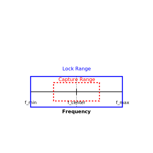
- Lock range: The maximum frequency deviation the PLL can track while maintaining phase lock, determined by the VCO's tuning range and loop gain.
- Capture range: The initial frequency offset over which the PLL can achieve lock, influenced by the loop filter's bandwidth.
Practical Implementation
Modern PLLs often employ charge-pump phase detectors and fractional-N synthesis for improved performance. Key applications include:
- Clock generation in microprocessors with jitter below 1 ps RMS
- Coherent demodulation in software-defined radios
- Frequency synthesis in RF transceivers (e.g., 5G mmWave systems)
Key Components of a PLL
A Phase-Locked Loop (PLL) is a feedback control system that synchronizes the phase and frequency of an output signal with a reference input signal. The core functionality of a PLL relies on several critical components, each contributing to its dynamic behavior and stability. Below, we examine these components in detail.
Phase Detector (PD)
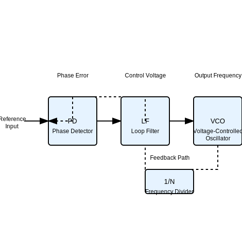
The phase detector compares the phase difference between the reference input signal and the feedback signal from the Voltage-Controlled Oscillator (VCO). The output of the phase detector is a signal proportional to the phase error, which drives the loop toward phase lock. Common types of phase detectors include:
- Analog multipliers (sinusoidal phase detectors): Produce an output proportional to the product of the input signals, generating a DC component that varies with the phase difference.
- Digital XOR gates: Output a pulse-width-modulated signal whose duty cycle corresponds to the phase difference.
- Sequential phase-frequency detectors (PFDs): Used in digital PLLs, providing both phase and frequency discrimination for faster acquisition.
The phase detector’s transfer function can be modeled as:
where Kd is the phase detector gain (in volts/radian) and Δϕ(t) is the phase error.
Loop Filter (LF)
The loop filter processes the phase detector output, removing high-frequency components and shaping the loop dynamics. The choice of loop filter determines the PLL’s stability, noise rejection, and transient response. Common configurations include:
- Passive RC filter: A simple first-order low-pass filter with transfer function:
- Active proportional-integral (PI) filter: Provides a pole at the origin and a zero to improve stability:
where τ1 = R1C and τ2 = R2C.
Voltage-Controlled Oscillator (VCO)
The VCO generates an output signal whose frequency is controlled by the loop filter’s output voltage. Its linearized frequency deviation is given by:
where ω0 is the free-running frequency and Kv is the VCO gain (in rad/s/V). The phase of the VCO output is the integral of frequency:
Frequency Divider (Optional)
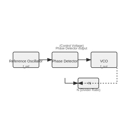
In applications requiring frequency multiplication, a frequency divider is inserted in the feedback path. The divider ratio N scales the VCO output frequency to match the reference:
This enables the PLL to synthesize higher frequencies while maintaining phase coherence with the reference signal.
Practical Considerations
Real-world PLLs must account for non-idealities such as:
- Phase detector dead zones: Regions where the phase detector output is insensitive to small phase errors, leading to increased jitter.
- VCO phase noise: Random fluctuations in the oscillator frequency, which degrade spectral purity.
- Loop delay: Propagation delays in the feedback path can destabilize high-bandwidth loops.
Advanced PLL designs incorporate techniques like charge pumps, adaptive bandwidth control, and fractional-N synthesis to mitigate these effects.
Lock and Capture Ranges
The performance of a Phase-Locked Loop (PLL) is critically defined by its lock range and capture range. These parameters determine the PLL's ability to synchronize with an input signal under varying conditions.
Lock Range
The lock range, also referred to as the tracking range, is the frequency range over which the PLL can maintain phase lock once synchronization is achieved. Mathematically, it is determined by the voltage-controlled oscillator (VCO) tuning range and the loop filter characteristics. For a second-order PLL with a proportional-integral (PI) loop filter, the lock range \(\Delta \omega_L\) is given by:
where:
- \(K_v\) is the VCO gain (rad/s/V),
- \(K_d\) is the phase detector gain (V/rad),
- \(F(0)\) is the DC gain of the loop filter.
In practical terms, the lock range is limited by the maximum frequency deviation the VCO can track without losing synchronization. If the input frequency drifts beyond this range, the PLL will unlock, and the loop must reacquire lock.
Capture Range
The capture range (or pull-in range) defines the maximum initial frequency difference between the input signal and the VCO output at which the PLL can achieve phase lock. Unlike the lock range, the capture range depends on the loop dynamics and transient response. For a second-order PLL with a passive lag filter, the capture range \(\Delta \omega_C\) is approximated by:
where:
- \(\zeta\) is the damping ratio,
- \(\omega_n\) is the natural frequency of the loop.
The capture range is typically smaller than the lock range, meaning the PLL must first pull the VCO frequency close enough to the input signal before full lock can be achieved.
Practical Implications
In real-world applications, such as frequency synthesizers and clock recovery circuits, the lock and capture ranges must be carefully designed to ensure robust operation. For instance:
- A wide lock range is essential in communication systems where input frequencies may vary due to Doppler shifts or oscillator drift.
- A narrow capture range may require an auxiliary frequency acquisition aid (e.g., a sweep circuit) to ensure initial lock.
The relationship between these ranges is often visualized in a PLL's frequency response curve, where the capture range forms a subset of the lock range.
Nonlinear Effects and Hysteresis
In practice, the transition between lock and unlock states exhibits hysteresis due to nonlinearities in the phase detector and loop filter. This means the PLL may remain locked even if the input frequency slightly exceeds the theoretical lock range, but once unlocked, it may require a larger frequency deviation to reacquire lock.
2. Analog PLLs
2.1 Analog PLLs
Analog phase-locked loops (PLLs) are closed-loop feedback systems that synchronize the phase and frequency of a voltage-controlled oscillator (VCO) with an input reference signal. The core components include a phase detector (PD), loop filter (LF), and VCO, each contributing to the system's dynamic response.
Phase Detector Dynamics
The phase detector compares the input reference signal θref(t) and the VCO output θvco(t), generating an error voltage ve(t) proportional to their phase difference. For a multiplier-based PD (e.g., analog mixer), the output is:
where Kd is the phase detector gain in volts/radian. For small phase errors, sin(Δθ) ≈ Δθ, linearizing the system.
Loop Filter Design
The loop filter, typically a passive RC or active op-amp configuration, suppresses high-frequency noise and sets the PLL's bandwidth. A second-order passive lag-lead filter with transfer function F(s) is common:
where τ1 = R1C and τ2 = R2C. The filter's pole and zero locations dictate stability and lock time.
Voltage-Controlled Oscillator
The VCO converts the filtered error voltage into a frequency deviation. Its output frequency ωvco(t) is:
where ω0 is the free-running frequency and Ko is the VCO gain in rad/s/V. The phase output integrates the frequency:
Linearized PLL Model
Combining the components, the open-loop transfer function G(s) in the Laplace domain is:
The closed-loop transfer function H(s) relates input phase Θref(s) to output phase Θvco(s):
For a second-order PLL with a lag-lead filter, this reduces to:
where ωn is the natural frequency and ζ is the damping ratio.
Applications and Tradeoffs
Analog PLLs excel in low-jitter clock recovery and FM demodulation. Key design tradeoffs include:
- Bandwidth vs. noise rejection: Wider bandwidth reduces lock time but increases susceptibility to input noise.
- Stability vs. tracking speed: Higher damping improves stability at the cost of slower step response.
- Reference spurs: Non-ideal PDs introduce harmonic artifacts, mitigated by higher-order filtering.
Modern implementations often replace analog components with digital equivalents (e.g., XOR gates for PDs), but analog PLLs remain prevalent in RF synthesis and high-speed serial links due to their superior phase noise performance.
2.2 Digital PLLs
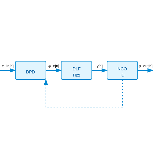
Digital phase-locked loops (DPLLs) replace analog components with digital equivalents, offering improved noise immunity, configurability, and integration with digital signal processors (DSPs). Unlike analog PLLs, which rely on voltage-controlled oscillators (VCOs) and continuous-time filters, DPLLs employ numerically controlled oscillators (NCOs), digital loop filters, and phase detectors implemented in logic or software.
Core Components of a Digital PLL
A DPLL consists of three primary blocks:
- Digital Phase Detector (DPD): Computes the phase difference between the input signal and the NCO output, typically using XOR gates, flip-flops, or digital signal processing algorithms.
- Digital Loop Filter (DLF): A finite impulse response (FIR) or infinite impulse response (IIR) filter that processes the phase error signal. Its coefficients determine loop bandwidth and stability.
- Numerically Controlled Oscillator (NCO): A digital synthesizer that generates a periodic waveform (e.g., sine or square wave) with a frequency controlled by a digital tuning word.
Mathematical Model of a DPLL
The linearized phase-domain model of a DPLL follows the same principles as an analog PLL but with discrete-time equations. The phase error φe[n] at sample n is:
The DLF applies a transfer function H(z) to the error signal, and the NCO integrates the filtered output:
where K0 is the NCO gain and y[n] is the DLF output. The loop’s stability criteria are derived from the z-domain characteristic equation:
Design Trade-offs and Applications
DPLLs excel in scenarios requiring precise frequency synthesis or clock recovery in digital systems (e.g., telecommunications, FPGA-based designs). Key trade-offs include:
- Quantization Effects: Finite bit-width in the NCO and phase detector introduces jitter, necessitating careful word-length selection.
- Loop Latency: Digital processing delays can reduce phase margin, limiting achievable bandwidth.
- Adaptive Filtering: DLF coefficients can be dynamically adjusted for rapid acquisition or low steady-state jitter.
Modern DPLLs often incorporate all-digital implementations (ADPLLs), where the oscillator is a digitally controlled ring or LC oscillator, further eliminating analog components.
Case Study: Clock Recovery in Serial Links
In high-speed serial communication (e.g., PCIe, USB), DPLLs extract clock signals from embedded data transitions. A bang-bang phase detector (BBPD) compares data edges to the NCO clock, and a digital filter averages the resulting early/late decisions to minimize bit error rate (BER).
The loop’s resolution is limited by the BBPD’s binary output, but oversampling and noise shaping mitigate this constraint.
2.3 All-Digital PLLs (ADPLLs)
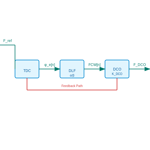
All-digital phase-locked loops (ADPLLs) replace traditional analog components with digital equivalents, offering superior programmability, scalability, and noise immunity in modern CMOS processes. Unlike mixed-signal PLLs, ADPLLs leverage time-to-digital converters (TDCs), digitally controlled oscillators (DCOs), and digital loop filters (DLFs) to achieve phase locking entirely in the digital domain.
Core Architecture
The ADPLL consists of three primary components:
- Time-to-Digital Converter (TDC): Measures the phase difference between the reference clock (Fref) and the DCO output (FDCO) with picosecond resolution. A vernier delay-line TDC is commonly used for high linearity.
- Digitally Controlled Oscillator (DCO): Replaces the VCO, with frequency tuning achieved through switched capacitor banks or varactor arrays. The DCO's gain (KDCO) is digitally calibrated.
- Digital Loop Filter (DLF): Implements proportional-integral (PI) control using adders and registers. Its coefficients (α, β) are programmable for bandwidth adjustment.
Mathematical Model
The phase-domain behavior of an ADPLL is modeled using a linearized difference equation. The phase error φe[n] at the n-th sample is:
The DLF processes the error to generate a frequency control word (FCW) for the DCO:
where α and β determine the loop's damping factor (ζ) and natural frequency (ωn).
Jitter Performance
ADPLL jitter is dominated by TDC quantization noise and DCO phase noise. The RMS jitter (σΔt) is derived from the TDC's least significant bit (LSB) resolution:
where TLSB is the TDC's time resolution. For a 10 ps LSB TDC at 100 MHz reference, this yields 0.29 ps RMS jitter.
Applications
- Wireless transceivers: ADPLLs enable fast frequency hopping in 5G NR and IEEE 802.11ax.
- Clock generators: Used in FPGA and ASIC clocking subsystems with < 1 ps RMS jitter.
- Digital RF synthesis: Direct digital synthesis (DDS) with ADPLLs achieves sub-Hz frequency resolution.
3. Phase Detector Characteristics
3.1 Phase Detector Characteristics
The phase detector (PD) is a critical component in a phase-locked loop (PLL), responsible for generating an error signal proportional to the phase difference between the input reference signal and the feedback signal from the voltage-controlled oscillator (VCO). The characteristics of the phase detector determine key PLL performance metrics, including lock range, tracking behavior, and noise immunity.
Linear vs. Non-Linear Phase Detectors
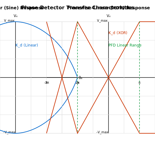
Phase detectors can be broadly categorized into linear and non-linear types. Linear phase detectors, such as analog multipliers (e.g., Gilbert cells), produce an output voltage Ve that is proportional to the sine of the phase difference θe between the input signals:
where Kd is the phase detector gain in volts per radian. For small phase differences (θe ≪ 1 rad), the approximation sin(θe) ≈ θe holds, rendering the PD linear within this region.
Non-linear phase detectors, such as digital XOR gates or flip-flop-based detectors, exhibit a piecewise-linear response. For example, an XOR phase detector outputs a duty-cycle-modulated signal whose average voltage is:
Phase Detector Gain and Linearity
The phase detector gain Kd is a crucial parameter that influences the PLL's loop dynamics. For an analog multiplier, Kd is derived from the mixer's conversion gain. For a digital PD, it depends on the supply voltage VDD and the output swing:
Non-linearities in the PD response introduce harmonic distortion and can limit the PLL's capture range. High-performance PLLs often employ phase-frequency detectors (PFDs), which combine phase detection with frequency discrimination to extend the lock range.
Phase-Frequency Detectors (PFDs)
A PFD generates UP and DOWN pulses whose widths correspond to the phase and frequency difference between the input signals. Its transfer characteristic is linear over a 4π range, with a gain given by:
where ICP is the charge pump current. PFDs are widely used in frequency synthesizers due to their ability to achieve zero static phase error and fast frequency acquisition.
Noise and Dead Zone Effects
Phase detectors contribute to PLL noise through Kd variations and quantization errors. Digital PDs are susceptible to dead zones, where small phase differences fail to generate corrective pulses. This is mitigated by ensuring minimal delay in the reset path of a PFD or by using high-speed comparators in analog PDs.
In high-frequency applications, the PD's propagation delay becomes significant, limiting the PLL's maximum operating frequency. Advanced CMOS processes and dynamic logic techniques are employed to minimize these delays.
3.2 Loop Filter Design
The loop filter in a Phase Locked Loop (PLL) is critical in determining system stability, transient response, and noise rejection. It converts the phase detector's output (typically a current or voltage pulse) into a smooth control signal for the Voltage-Controlled Oscillator (VCO). The design involves selecting appropriate filter topology and component values to meet bandwidth, phase margin, and damping requirements.
Transfer Function and Filter Types
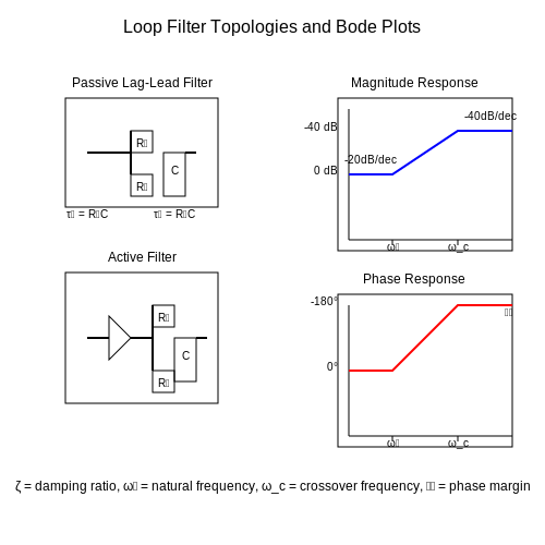
The loop filter's transfer function F(s) shapes the PLL's open-loop response. For a second-order PLL, the most common loop filter is the passive lag-lead filter, whose transfer function is:
where τ1 = R1C and τ2 = R2C. The loop's natural frequency ωn and damping factor ζ are derived as:
Here, Kv is the VCO gain, Kd is the phase detector gain, and N is the feedback divider ratio.
Active vs. Passive Loop Filters
Passive filters are simple and power-efficient but suffer from limited tuning range and higher reference spur levels. Active filters, often implemented with operational amplifiers, provide higher gain and better spur suppression but introduce additional noise and power consumption.
The transfer function of a second-order active filter is:
Active filters allow independent control of pole-zero placement, improving loop dynamics.
Design Trade-offs and Stability
Key considerations in loop filter design include:
- Bandwidth: A higher loop bandwidth improves transient response but increases susceptibility to noise.
- Phase Margin: Typically set between 45°–60° to ensure stability.
- Damping Factor: A value of 0.707 (critical damping) minimizes overshoot while maintaining responsiveness.
To ensure stability, the open-loop phase must not approach −180° within the bandwidth. The Bode plot of the loop gain G(s) = K_v K_d F(s) / (Ns) should exhibit sufficient phase margin.
Component Selection and Practical Implementation
For a given bandwidth ωc and phase margin ϕm, the filter components can be calculated as:
Capacitor C is often chosen first based on noise and size constraints, followed by resistor calculations. High-quality, low-leakage capacitors (e.g., NP0/C0G ceramics) are preferred to minimize drift.
Higher-Order Filters and Spur Suppression
For applications requiring stringent reference spur attenuation, third-order filters (with an additional pole) are employed. The transfer function becomes:
where τ3 = R3C2. The added pole must be placed sufficiently far from the loop bandwidth to avoid destabilizing the system.
Loop filter design remains a balance between stability, noise rejection, and transient performance, often requiring iterative simulation and optimization in tools like SPICE or MATLAB.
3.3 Voltage-Controlled Oscillator (VCO) Dynamics
The voltage-controlled oscillator (VCO) is a critical component in phase-locked loop (PLL) systems, converting an input control voltage into a corresponding output frequency. Its dynamics determine key performance metrics such as tuning range, linearity, and phase noise.
Frequency Tuning and Transfer Function
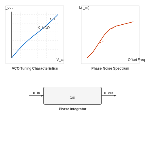
The VCO's output frequency fout is a function of the input control voltage Vctrl:
where f0 is the free-running frequency (output at Vctrl = 0) and KVCO is the tuning sensitivity in Hz/V. The phase output θout is the integral of frequency:
In the Laplace domain, the VCO acts as an integrator for phase:
Nonlinearity and Tuning Range
Practical VCOs exhibit nonlinear tuning characteristics due to varactor diode capacitance-voltage (C-V) dependence. The modified frequency-voltage relationship becomes:
where α and β represent second- and third-order nonlinear coefficients. The tuning range Δf is bounded by:
where fmax and fmin are determined by the varactor's reverse breakdown voltage and minimum capacitance.
Phase Noise and Jitter
VCO phase noise L(fm) follows Leeson's model:
where:
- F = noise factor
- Q = resonator quality factor
- fc = flicker noise corner frequency
- fm = offset from carrier
Jitter σt relates to phase noise through:
Design Trade-offs
Key VCO design considerations include:
- Tuning linearity vs. range: Wider ranges increase nonlinearity.
- Phase noise vs. power: Higher Q resonators improve noise but limit tuning.
- Supply sensitivity: Poor power supply rejection ratio (PSRR) introduces spurious modulation.
Modern VCOs often employ LC-tank topologies with switched capacitor banks for discrete coarse tuning and varactors for fine continuous tuning, achieving both wide range and low phase noise.
3.4 Stability Analysis
The stability of a Phase Locked Loop (PLL) is critical to ensuring reliable operation, particularly in applications requiring precise frequency and phase tracking. Stability analysis involves examining the loop dynamics to prevent oscillations, excessive overshoot, or divergence. The primary tool for this analysis is the open-loop transfer function, which provides insight into the system's phase margin and gain margin.
Open-Loop Transfer Function
The open-loop transfer function \( G(s)H(s) \) of a PLL is derived from the product of the phase detector gain \( K_d \), loop filter transfer function \( F(s) \), and voltage-controlled oscillator (VCO) gain \( K_o \), divided by \( s \):
For a second-order PLL with a passive lag-lead filter, \( F(s) \) is given by:
where \( \tau_1 = R_1C \) and \( \tau_2 = R_2C \). Substituting this into the open-loop transfer function yields:
Phase Margin and Stability Criteria
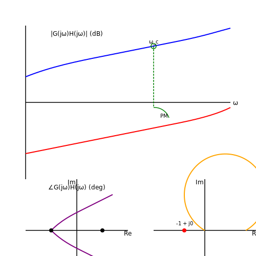
The phase margin (PM) is a key metric for stability, defined as the additional phase shift required at the unity-gain frequency to bring the system to the verge of instability. A phase margin greater than \( 45^\circ \) is typically desired for robust stability. The phase margin is calculated as:
where \( \omega_c \) is the crossover frequency where \( |G(j\omega_c)H(j\omega_c)| = 1 \). For the second-order PLL, the phase margin can be approximated as:
Root Locus and Nyquist Analysis
For a more comprehensive stability assessment, root locus and Nyquist methods are employed. The root locus plots the poles of the closed-loop transfer function as the loop gain varies, revealing stability boundaries. The Nyquist criterion evaluates encirclements of the \(-1 + j0\) point in the complex plane to determine stability.
For a second-order PLL, the closed-loop transfer function is:
The characteristic equation \( 1 + G(s)H(s) = 0 \) determines the system poles:
Stability requires all poles to lie in the left-half plane (LHP), which is guaranteed if all coefficients are positive—a condition satisfied for typical PLL parameters.
Effect of Loop Bandwidth on Stability
The loop bandwidth \( \omega_n \) (natural frequency) and damping factor \( \zeta \) are critical to transient response and stability. For a second-order PLL:
A higher \( \omega_n \) improves tracking speed but reduces phase margin, while a higher \( \zeta \) reduces overshoot at the cost of slower response. Practical designs balance these trade-offs, often targeting \( \zeta \approx 0.707 \) for optimal damping.
Practical Stability Considerations
In real-world PLLs, non-idealities such as:
- Phase detector dead zones,
- VCO nonlinearities,
- Power supply noise,
- Component tolerances
can degrade stability. Monte Carlo simulations and worst-case analysis are often used to validate robustness across parameter variations. Additionally, higher-order loops (e.g., third-order PLLs for reduced jitter) require careful compensation to avoid instability.
4. Frequency Synthesis
4.1 Frequency Synthesis
Frequency synthesis in phase-locked loops (PLLs) enables the generation of highly stable output signals with precise frequency control, critical in applications such as wireless communication, radar systems, and clock generation. The core principle relies on locking the PLL output frequency fout to a reference frequency fref while allowing programmable scaling via feedback division.
Mathematical Basis of Frequency Synthesis
The output frequency of a PLL-based synthesizer is determined by the feedback divider ratio N:
where N is an integer in integer-N synthesizers or a fractional value in fractional-N architectures. The phase detector ensures the VCO output, when divided by N, matches fref in both frequency and phase.
Integer-N vs. Fractional-N Synthesis
Integer-N synthesis provides discrete frequency steps equal to fref, limiting resolution. For example, a 1 MHz reference permits only integer multiples (e.g., 1 GHz requires N = 1000). Spurs occur at offsets of fref due to periodic phase corrections.
Fractional-N synthesis achieves finer resolution by dynamically modulating N between integers (e.g., alternating between 100 and 101 to approximate N = 100.5). This introduces fractional spurs, mitigated through delta-sigma modulation or dithering techniques.
Phase Noise Considerations
The synthesized output inherits phase noise from the reference oscillator, VCO, and feedback divider. The total phase noise L(f) at offset fm is approximated by:
where Lref and LVCO are the reference and VCO phase noise contributions, respectively. Higher N degrades in-band noise due to the 20log10(N) term.
Practical Implementation Challenges
- Reference Spurs: Leakage from the phase detector or charge pump creates spurious tones at fref offsets. Proper loop filter design and charge pump matching minimize these artifacts.
- Lock Time: Trade-offs exist between loop bandwidth (faster locking) and phase noise suppression. Adaptive bandwidth techniques optimize transient response.
- Divider Nonlinearity: High-speed prescalers in the feedback path introduce jitter, requiring careful high-frequency design.
Advanced Techniques
Modern synthesizers employ multi-loop architectures to decouple resolution from reference frequency constraints. For instance, a dual-loop PLL might combine a coarse-tuned high-frequency loop with a fine-resolution auxiliary loop. Direct digital synthesis (DDS) hybrids further enhance agility by replacing the feedback divider with a numerically controlled oscillator (NCO).
4.2 Clock Recovery in Communication Systems
Clock recovery is a critical function in digital communication systems, where the receiver must extract timing information from the incoming data stream to correctly sample and decode the transmitted symbols. A Phase-Locked Loop (PLL) is often employed for this purpose, synchronizing a local oscillator to the embedded clock signal within the data.
Mathematical Basis of Clock Recovery
In a typical communication system, the received signal r(t) can be modeled as:
where ak represents the transmitted symbols, p(t) is the pulse shape, T is the symbol period, τ is the timing offset, and n(t) is additive noise. The PLL must estimate and compensate for τ to recover the clock.
Early-Late Gate Synchronizer
A common clock recovery technique is the Early-Late Gate Synchronizer, which compares the energy of the received signal at slightly early and late sampling instants. The timing error e(t) is derived as:
where Δ is the timing offset between early and late samples. The PLL adjusts the local clock to drive e(t) to zero, achieving synchronization.
Phase Detector in Clock Recovery
For non-data-aided systems, a nonlinear phase detector such as the Mueller and Müller algorithm is often used. The error signal is computed as:
where âk are the detected symbols and ŷk are the sampled outputs. This method minimizes inter-symbol interference (ISI) by aligning sampling instants with the maximum eye opening.
Jitter Tolerance and Bandwidth Considerations
The PLL's loop bandwidth must be carefully selected to balance jitter tracking and noise suppression. A narrow bandwidth reduces noise but may fail to track high-frequency jitter, while a wide bandwidth increases susceptibility to noise. The optimal bandwidth depends on the application's jitter spectrum and signal-to-noise ratio (SNR).
Applications in Modern Communication Systems
Clock recovery PLLs are essential in:
- Optical communication (e.g., SONET/SDH networks)
- Serial data links (e.g., PCIe, USB, Ethernet)
- Wireless systems (e.g., OFDM synchronization)
In high-speed SerDes (Serializer/Deserializer) interfaces, advanced techniques like bang-bang phase detection and digital PLLs are employed to achieve sub-picosecond jitter performance.
4.3 Demodulation of FM and PM Signals
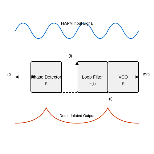
Phase-locked loops (PLLs) are widely used for demodulating frequency-modulated (FM) and phase-modulated (PM) signals due to their ability to track the instantaneous phase and frequency of the input signal. The PLL acts as a coherent demodulator, recovering the original baseband signal by locking onto the carrier and extracting the modulating information.
FM Demodulation Using a PLL
In FM demodulation, the PLL tracks the frequency variations of the input signal. The voltage-controlled oscillator (VCO) in the PLL adjusts its frequency to match the input signal, and the control voltage applied to the VCO becomes a replica of the original modulating signal.
where ωVCO(t) is the VCO output frequency, ωc is the carrier frequency, Kv is the VCO gain, and e(t) is the error voltage. The demodulated signal is obtained from the loop filter output:
where ϕin(t) is the phase of the input FM signal. The PLL effectively differentiates the phase to recover the frequency modulation.
PM Demodulation Using a PLL
For PM signals, the PLL locks onto the phase variations of the input signal. The VCO control voltage directly represents the phase-modulating signal:
The demodulated signal is obtained directly from the loop filter output:
where e(t) is proportional to the phase difference between the input and VCO signals.
Practical Considerations
The performance of PLL-based demodulators depends on several factors:
- Loop bandwidth: Must be wide enough to track the highest modulating frequency but narrow enough to reject noise.
- VCO linearity: Nonlinearities in the VCO transfer function introduce distortion in the demodulated signal.
- Phase detector characteristics: The type of phase detector (e.g., multiplier, XOR, or sequential) affects the demodulation linearity and noise performance.
Applications in Communication Systems
PLL-based FM demodulators are commonly used in:
- FM radio receivers (e.g., quadrature detectors replaced by PLLs in modern ICs)
- Satellite communication systems for demodulating wideband FM signals
- Data transmission systems using FSK (frequency-shift keying) modulation
For PM signals, PLL demodulators find applications in:
- Phase-modulated digital communication systems (e.g., BPSK, QPSK)
- Coherent optical communication systems
- Radar and sonar systems for phase-encoded signals
Mathematical Analysis of PLL Demodulation
The operation of a PLL as a demodulator can be analyzed using linear system theory when the loop is locked. The transfer function from the input phase to the VCO control voltage is:
where Kd is the phase detector gain, F(s) is the loop filter transfer function, and Kv is the VCO gain. For FM demodulation, we're interested in the response to frequency variations:
This shows that the PLL naturally acts as a demodulator for frequency-modulated signals, with the loop filter shaping the noise and distortion characteristics.
Noise Performance
The signal-to-noise ratio (SNR) of a PLL-based FM demodulator is given by:
where Δf is the frequency deviation, fm is the maximum modulating frequency, and (C/N)in is the carrier-to-noise ratio at the input. This demonstrates the well-known FM improvement factor that increases with the square of the deviation ratio.
4.4 Motor Speed Control
Fundamentals of PLL-Based Motor Control
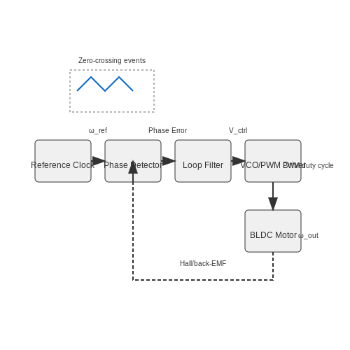
Phase-locked loops (PLLs) are widely used in motor speed control due to their ability to precisely synchronize an output signal with a reference. In motor applications, the PLL locks onto the back-electromotive force (EMF) or encoder pulses to regulate rotational speed. The core components—phase detector, loop filter, voltage-controlled oscillator (VCO), and feedback divider—form a closed-loop system that minimizes phase error between the reference and motor-generated signal.
where ωout is the output frequency (proportional to motor speed), KVCO is the VCO gain, and Vctrl is the filtered error voltage from the phase detector.
Implementation with Brushless DC Motors
For brushless DC (BLDC) motors, the PLL synchronizes with Hall-effect sensor signals or sensorless back-EMF zero-crossing events. The phase detector compares the rising edges of the reference clock (setpoint) and motor feedback signals. The resulting error voltage is filtered and fed to the VCO, which adjusts the PWM duty cycle driving the motor.
Mathematical Analysis of Lock Range and Stability
The PLL's lock range ΔωL must exceed the motor's maximum speed deviation. For a second-order PLL with a proportional-integral (PI) loop filter:
where KPD is the phase detector gain, τ1 and τ2 are filter time constants, and ζ is the damping ratio (typically 0.7–1.0 for stable operation).
Advanced Techniques: Sensorless Control
Modern implementations eliminate Hall sensors by extracting speed information from back-EMF harmonics using:
- Adaptive filtering to suppress PWM switching noise
- Sliding-mode observers for robust zero-crossing detection
- Kalman filters in high-noise environments
where ŵ is the estimated speed, Tzc is the zero-crossing period, Vemf is the back-EMF voltage, and Ke is the motor's voltage constant.
Practical Considerations
Key design challenges include:
- Nonlinearities in motor torque-speed characteristics
- Phase jitter due to cogging torque in permanent magnet motors
- Trade-offs between response time (wide bandwidth) and noise rejection
Field-oriented control (FOC) systems often integrate PLLs with Clarke/Park transforms for optimal dynamic performance. The PLL's bandwidth should be 5–10× lower than the current control loop bandwidth to avoid instability.
5. Noise and Jitter in PLLs
5.1 Noise and Jitter in PLLs
Sources of Noise in Phase-Locked Loops
Noise in PLLs arises from both intrinsic and extrinsic sources, degrading phase accuracy and spectral purity. The primary contributors include:
- Thermal noise in resistors and active devices, modeled as additive white Gaussian noise (AWGN).
- Flicker (1/f) noise in oscillators and amplifiers, dominant at low frequencies.
- Power supply noise coupling through substrate or rails, inducing frequency modulation.
- Quantization noise in digital PLLs due to finite resolution of time-to-digital converters (TDCs).
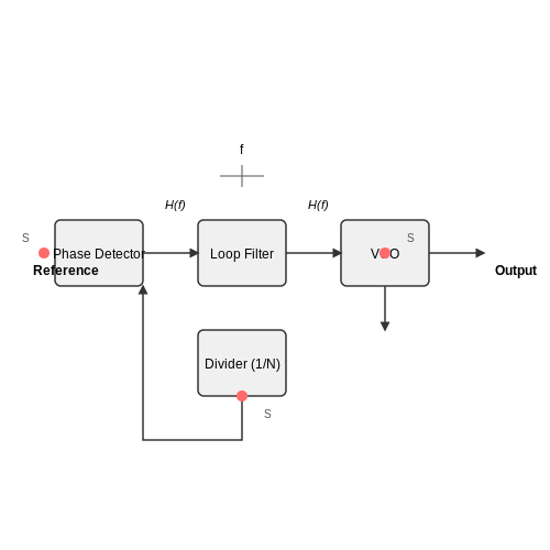
The total phase noise power spectral density (PSD) at the PLL output combines these contributions through the transfer functions of individual blocks:
where \( H_{\text{OL}} \) and \( H_{\text{CL}} \) are open-loop and closed-loop transfer functions respectively, and \( N \) is the divider ratio.
Jitter Mechanisms and Modeling
Jitter manifests as temporal deviations in zero-crossings of the output waveform. For a PLL, the primary jitter components are:
- Periodic jitter (deterministic): Caused by supply ripple or coupling from periodic signals.
- Random jitter (stochastic): Arises from phase noise integration over the observation interval.
The RMS period jitter \( \sigma_{\text{PER}} \) relates to phase noise \( \mathcal{L}(f) \) through:
where \( T_0 \) is the nominal clock period, and \( f_1 \), \( f_2 \) define the integration bandwidth.
Phase Noise to Jitter Conversion
For a free-running VCO, phase noise dominates the jitter accumulation. The cycle-to-cycle jitter \( \sigma_{\text{cc}} \) is derived by integrating the phase noise PSD:
In locked condition, the PLL's low-pass characteristic suppresses VCO noise within the loop bandwidth \( f_{\text{BW}} \), while reference noise dominates at offsets below \( f_{\text{BW}} \).
Noise Transfer Functions in PLLs
Each noise source propagates through distinct transfer functions:
- Reference noise: High-pass filtered by \( 1 - H_{\text{CL}}(f) \).
- VCO noise: Low-pass filtered by \( H_{\text{CL}}(f) \).
- Divider noise: Follows the same transfer function as reference noise, scaled by \( 1/N \).
The loop filter's pole-zero placement critically determines the integrated jitter. A type-II PLL with charge pump exhibits:
where \( \omega_z = 1/(R_1 C_1) \) sets the zero frequency for stability.
Design Techniques for Noise Reduction
Advanced PLLs employ several methods to mitigate noise and jitter:
- Subsampling phase detection: Reduces charge pump current mismatch and reference spur feedthrough.
- Dithering: Randomizes fractional-N divider modulus to convert spurs into broadband noise.
- Supply regulation: Low-noise LDOs isolate VCO and dividers from power bus fluctuations.
In fractional-N PLLs, delta-sigma modulation shapes quantization noise, pushing it to high frequencies where the loop filter attenuates it. The resulting phase noise improvement is:
where OSR is the oversampling ratio and \( n \) is the modulator order.
5.2 Fractional-N PLLs
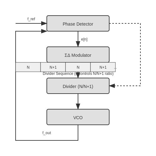
Fractional-N phase-locked loops (PLLs) extend the capabilities of integer-N PLLs by allowing frequency synthesis with fractional division ratios. This enables finer frequency resolution without compromising loop bandwidth or phase noise performance. The key innovation lies in dynamically modulating the divider value between two integers, N and N+1, such that the average division ratio becomes N + α, where α is a fractional value between 0 and 1.
Mathematical Basis of Fractional Division
The effective division ratio is achieved by toggling the divider between N and N+1 in a controlled sequence. If the divider spends k cycles at N+1 and m-k cycles at N over a total of m cycles, the average division ratio is:
This allows synthesizing frequencies at steps smaller than the reference frequency f_{ref}. For example, with N = 10 and k/m = 0.25, the output frequency becomes:
Sigma-Delta Modulation for Fractional Control
A sigma-delta modulator (ΣΔ) is typically employed to shape the quantization noise introduced by the fractional division process. The modulator dynamically adjusts the divider sequence to push phase error noise to higher frequencies, where it can be filtered by the PLL loop. A first-order ΣΔ modulator follows the recursion:
where e[n] is the accumulated error, α is the fractional part, and d[n] determines whether the divider uses N or N+1 at each step.
Spur Suppression Techniques
Fractional-N PLLs introduce spurious tones due to periodic phase corrections. These spurs can be mitigated through:
- Randomized divider sequencing to break periodicity.
- Higher-order ΣΔ modulators to further shape noise away from the carrier.
- Phase interpolation to smooth abrupt phase steps.
Applications in Modern Systems
Fractional-N PLLs are indispensable in wireless communication systems, where they enable precise channel spacing (e.g., LTE, 5G) and fast frequency hopping. They also find use in high-speed data converters and radar systems, where fine frequency resolution and low jitter are critical.
5.3 PLLs in RF and Microwave Systems
Phase Noise and Jitter in RF PLLs
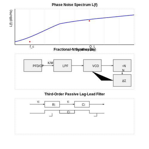
In RF and microwave applications, phase noise and jitter are critical performance metrics. Phase noise, represented as L(f), quantifies spectral purity by measuring the power of phase fluctuations in a 1 Hz bandwidth at an offset frequency f from the carrier. The Leeson-Cutler model provides a semi-empirical approximation for phase noise in a PLL:
where F is the noise figure, k is Boltzmann’s constant, T is temperature, Psig is the signal power, f0 is the oscillator’s center frequency, QL is the loaded quality factor, and fc is the flicker noise corner frequency. Jitter, the time-domain counterpart, is derived by integrating phase noise over the relevant bandwidth:
Frequency Synthesis Techniques
PLL-based frequency synthesizers in RF systems often employ fractional-N or integer-N architectures. Fractional-N synthesizers achieve finer frequency resolution by dynamically modulating the division ratio N using a delta-sigma modulator. The output frequency is given by:
where K/M represents the fractional part. This introduces quantization noise, mitigated through high-order delta-sigma modulation and careful loop filter design.
Loop Filter Design for Wideband Applications
Wideband RF PLLs require loop filters balancing stability, phase margin, and noise suppression. A third-order passive lag-lead filter is common:
where τ2 = R2C2 and τ3 = R2(C1 || C2). The phase margin ϕm must exceed 45° to avoid peaking in the transfer function.
Applications in Modern RF Systems
- 5G mmWave Beamforming: PLLs synchronize local oscillators in phased-array antennas, requiring sub-100 fs jitter for coherent signal combining.
- Satellite Communications: Ultra-low phase noise PLLs (< -110 dBc/Hz at 10 kHz offset) mitigate Doppler effects in Ka-band transponders.
- Radar Systems: Fast-locking PLLs (< 10 μs) enable frequency-agile waveforms for FMCW radar chirp generation.
Advanced Topologies: Sub-Sampling PLLs
Sub-sampling PLLs (SSPLLs) reduce phase noise by directly sampling the VCO output with the reference clock, bypassing the traditional phase-frequency detector (PFD). The sampling operation creates an error voltage proportional to phase difference:
where Asamp is the sampling gain. SSPLLs achieve phase noise below -150 dBc/Hz at 1 MHz offset in 28 nm CMOS implementations.
Thermal and Packaging Considerations
At microwave frequencies, substrate coupling and thermal gradients degrade PLL performance. Key countermeasures include:
- Differential VCO layouts with guard rings to minimize substrate noise injection.
- Low-thermal-resistance packages (e.g., flip-chip BGA) to stabilize oscillator temperature.
- On-die temperature sensors with adaptive bias compensation loops.
6. Recommended Textbooks
6.1 Recommended Textbooks
- PDF Phase-Locked Loop Engineering Handbook for Integrated Circuits — 1.2 Phase-Lock Loop Literature 5 1.2.1 Books 5 1.2.2 Articles 6 1.2.3 Background Books 6 1.2.4 Web Sites 7 1.3 Loop Classifications 7 1.4 Example Applications 7 1.4.1 History 8 1.4.2 Doppler Radar 9 1.4.3 Satellite Communications 10 1.4.4 Cellular Phones 10 1.4.5 Telecommunications Systems 11 Questions 12 References 13 CHAPTER 2 System Analysis 15
- Phase‐Locked Loops: System Perspectives and Circuit Design Aspects ... — 1.1 Phase-LockTechnique 1 1.2 KeyPropertiesandApplications 2 1.2.1 FrequencySynthesis 3 1.2.2 Clock-and-DataRecovery 3 1.2.3 Synchronization 4 1.2.4 ModulationandDemodulation 5 1.2.5 CarrierRecovery 6 1.2.6 FrequencyTranslation 6 1.3 OrganizationandScopeoftheBook 6 Bibliography 7 Part I Phase-Lock Basics 9 2 Linear Model and Loop Dynamics 11 2. ...
- PDF Phase Lock Loops and Frequency Synthesis — 10.4 Digital Phase-locked Loops (DPLLs) 249 10.4.1 Digital Phase-locked Loops of the First Order 249 10.4.2 Digital Phase-locked Loops of the Second Order 250 10.5 Transient Response Evaluation for Steady and Periodic Changes of Input Phase and Frequency 252 10.6 Loop Noise Bandwidth of Digital PLLs 253 References 254. 11 PLLs in Frequency ...
- PHASE-LOCK BASICS - Wiley Online Library — Wiley also publishes its books in a variety of electronic formats. Some content that appears in print may ... 1.2 Why Use a Phase-Locked Loop? / 3 1.3 Scope of this Book / 4 1.4 Basic Loop / 5 1.5 Phase Definitions / 6 1.6 Phase Detector / 8 1.7 Combined Gain / 10 1.8 Operating Range / 11 1.9 Units and the Laplace Variable s /13 vii.
- PDF Lecture 19 Phase Locking & Timing/Carrier Recovery - Stanford University — The Phase Lock Loop ... Section 6.1.2.2. Phase Locking March 12, 2026 Section 6.2 12. ... §ET presumes carrier is already known, phase-locked. §The "squaring" generalizes to complex magnitude (squared). §Otherwise, the concept remains the same. Section 6.3.1. March 12, 2026
- PDF DIGITAL PHASE LOCK LOOPS - download.e-bookshelf.de — Digital Phase Lock Loops Architectures and Applications by SALEH R. AL-ARAJI ZAHIR M. HUSSAIN ... 6 1.3.3 PLLanalysis ..... 10 1.4 Conclusions ..... 13 2 Digital Phase Lock Loops 15 ... electronic engineering from Manchester University, UK, in 1987, and the Ph.D. Loops ...
- Phase Locked Loops (Microwave and RF Techniques and Applications, 6 ... — Phase Locked Loops (Microwave and RF Techniques and Applications, 6) [Encinas, J.] on Amazon.com. *FREE* shipping on qualifying offers. Phase Locked Loops (Microwave and RF Techniques and Applications, 6) ... New Releases Best Sellers & More Amazon Book Clubs Children's Books Textbooks Best Books of the Month Your Company Bookshelf Books ...
- PDF Design of CMOS Phase-Locked Loops - Cambridge University Press & Assessment — 978-1-108-49454- — Design of CMOS Phase-Locked Loops Behzad Razavi Frontmatter ... Press & Assessment www.cambridge.org Design of CMOS Phase-Locked Loops Using a modern, pedagogical approach, this textbook gives s tudents and engineers a comprehensive and ... provoking examples that demonstrate best practices and com
- Phase-Locked Loops: Principles and Practice - amazon.com — Phase-Locked Loop Design is a concise guide to both the theory and design of phase-locked loop circuits. It is written from an engineering point of view, with numerous illustrations, block diagrams, example circuits and experimental results-many based on the author's personal experience-and use of engineering analytical methods, such as signal flow graphs and and Laplace transforms.
6.2 Research Papers and Articles
- Phase‐Locked Loops: System Perspectives and Circuit Design Aspects ... — 1.1 Phase-LockTechnique 1 1.2 KeyPropertiesandApplications 2 1.2.1 FrequencySynthesis 3 1.2.2 Clock-and-DataRecovery 3 1.2.3 Synchronization 4 1.2.4 ModulationandDemodulation 5 1.2.5 CarrierRecovery 6 1.2.6 FrequencyTranslation 6 1.3 OrganizationandScopeoftheBook 6 Bibliography 7 Part I Phase-Lock Basics 9 2 Linear Model and Loop Dynamics 11 2. ...
- PDF Phase Lock Loops and Frequency Synthesis — 10.4 Digital Phase-locked Loops (DPLLs) 249 10.4.1 Digital Phase-locked Loops of the First Order 249 10.4.2 Digital Phase-locked Loops of the Second Order 250 10.5 Transient Response Evaluation for Steady and Periodic Changes of Input Phase and Frequency 252 10.6 Loop Noise Bandwidth of Digital PLLs 253 References 254. 11 PLLs in Frequency ...
- PDF THRESHOLD ANALYSIS OF PHASE LOCKED LOOPS - NASA Technical Reports ... — Phase Locked Loop VI. COMPARISON OF EXPERDENTAL AND THEORETICAL RESULTS 6.1 6.2 Second Order Phase Locked Loop 6.3 Third Order Phase Locked Loop First Order Phase Locked Loop 6.3.1 A Look at the Bounds of the Noise Mode 1 VII. CONCLUSION 7.1 Conclusions 7.2 Application of Method to any Deterministic Modulation 7.3 Suggestions for Future Work
- PDF Design and Implementation of Digital PLL using Self Correcting ... - IJERA — M.Mohan Babu Int. Journal of Engineering Research and Applications www.ijera.com ISSN : 2248-9622, Vol. 4, Issue 8( Version 3), August 2014, pp.196-199 ... Phase locked loops were initially written but not designed. The previous analog design consists of ... Further improvement in this paper is to apply phase lock for analog signals by using ...
- PDF Study of Optical Phase Lock Loops and the Applications in Coherent Beam ... — A phase lock loop (PLL) is a negative feedback control system that fixes the frequency and phase of a local oscillator in relation to the frequency and phase of a "reference" signal. Electronic phase lock loop has been studied for more than half a century and has
- Research on phase-locked loop technique based on three-dimensional ... — Research on phase-locked loop technique based on three-dimensional coordinate transformation. Guangjun Tan 1, Zhi Chen 1, Wei Zhao 1 and Xiaofeng Sun 1. ... The experimental platform of the digital control system designed in this paper for phasor detection technique is shown in figure 6. This experimental platform uses two printed circuit ...
- PDF DIGITAL PHASE LOCK LOOPS - download.e-bookshelf.de — of the loop. Organization of Book The first chapter provides a general review of phase-lock loops. Chapter two reviews the uniform and non-uniform type Digital Phase Lock Loops (DPLL). Chapter three covers the Time Delay Digital Tanlock Loop (TDTL) and it's convergence behavior. The following two chapters will focus on the Hilbert
- Effect of phase‐locked loop on small‐signal perturbation modelling and ... — For three-phase LCL-type inverter connected to weak grid, the bandwidth and dynamics of phase-locked loop (PLL) directly affect small-signal perturbation modelling, which causes the control dq frame of PLL being no longer aligned with the system dq frame of weak grid. Thus, considering the effect of PLL, a small-signal perturbation admittance model is firstly built.
- Basic Concepts of a Phase-Locked Loop Control System - ResearchGate — This paper presents fractional-N sigma-delta phase locked loop (PLL) applications and design. Applications focus primarily on wireless communication and clock synthesizers. Fractional-N PLL ...
- PDF A low power CMOS design of an all digital phase locked loop — A Low Power CMOS Design of An All Digital Phase Locked Loop A Thesis Presented by Jun Zhao to The Department of Department of Electrical and Computer Engineering
6.3 Online Resources and Tutorials
- PDF Phase-Locked Loops: A Control Centric Tutorial — Phase-Locked Loops: A Control Centric Tutorial Daniel Abramovitch Agilent Laboratories Communications and Optics Research Lab 3500 Deer Creek Road, M/S: 25U-9 Palo Alto, CA 94304 Phone: (650) 485-3806 FAX: (650) 485-4080 E-mail: [email protected] June 24, 2003 Abstract This paper will present a tutorial on phase-locked loops from a control ...
- PDF PHASE-LOCKED LOOPS FOR - iczhiku.com — TheEarly Historyof Phase-Locked Loops 1.1 History A browse through the phase-locked loop literature of the past is humbling. Although we often consider phase-locked loops as relatively new structures, historical literature dates the concept as early as 1919 [2]. Vincent [2] and Appleton [3] experimented and analyzed, respectively, the
- Phase-Locked Loops: System Perspectives and Circuit Design Aspects — Phase-Locked Loops Discover the essential materials for phase-locked loop circuit design, from fundamentals to practical design aspects A phase-locked loop (PLL) is a type of circuit with a range of important applications in telecommunications and computing. It generates an output signal with a controlled relationship to an input signal, such as an oscillator which matches the phases of input ...
- PDF Digital Phase Lock Loops - Springer — Digital Phase Lock Loops ›springer.com Digital phase lock loops are critical components of many communication, signal processing and control systems. Th is exciting new book covers various types of digital phase lock loops. It presents a comprehensive coverage of a new class of digital phase lock loops called the time delay tanlock loop (TDTL).
- PDF Design of CMOS Phase-Locked Loops - Cambridge University Press & Assessment — locked loops, clock and data recovery circuits, and frequen cy dividers; tutorial chapters on high-performance oscillator design, covering fundamentals to advanced topo logies; and extensive use of circuit simulations to teach design mentality, highlight design aws, and connect theory with practice. Offering over 200 thought-
- Phase-locked loop - Wikipedia — Figure 1. Simple analog phase locked loop. A simple analog PLL is an electronic circuit consisting of a variable frequency oscillator and a phase detector in a feedback loop (Figure 1). The oscillator generates a periodic signal V o with frequency proportional to an applied voltage, hence the term voltage-controlled oscillator (VCO). The phase detector compares the phase of the VCO's output ...
- Digital Phase-Locked Loop - SpringerLink — Department of Electronics and Communication Technology, Gauhati University, Guwahati, Assam, India. Kandarpa Kumar Sarma. ... Phase-locked loop-based frequency synthesizers make use of frequency dividers to generate a frequency, which is a multiple of a reference frequency. Frequency dividers can be implemented for both analog and digital ...
- Tan-Sun Transformation-Based Phase-Locked Loop in Detection of ... - MDPI — When three-phase voltages are polluted with unbalance, DC offsets, or higher harmonics, it is a challenge to quickly detect their parameters such as phases, frequency, and amplitudes. This paper proposes a phase-locked loop (PLL) for the three-phase non-ideal voltages based on the decoupling network composed of two submodules. One submodule is used to detect the parameters of the fundamental ...
- A robust phase-locked loop against fundamental ... - ScienceDirect — This paper proposes a phase-locked loop scheme based on two equal blocks in series. Each block is composed of a positive-sequence estimator and the SRF-PLL. The sequence estimator relies on the description of the phase voltages in the stationary αβ frame, as suggested in [32]. However, its harmonic rejection capability is improved through the ...
- 14 results in SearchWorks catalog - searchworks-lb.stanford.edu — Chat with us (limited to Stanford community) Email a reference question Using SearchWorks Connection Connect to e-resources Report a connection problem If we don't have it Interlibrary borrowing System status. Advanced search Course reserves; Selections (0) Clear all lists. Search Constraints