Touch Activated Light Circuit
1. Basic Concept and Applications
1.1 Basic Concept and Applications
Fundamental Operating Principle
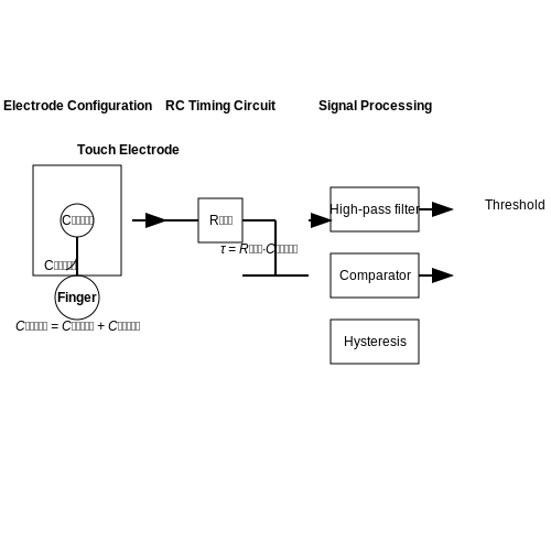
The touch-activated light circuit operates on the principle of capacitive sensing, where a conductive surface (touch electrode) detects changes in capacitance caused by the proximity or contact of a human finger. The human body acts as a conductive medium, introducing an additional capacitance (Ctouch) to the system. This change is processed by an active circuit, typically a relaxation oscillator or charge-transfer sensor, to trigger a switching mechanism.
Here, Cstray represents the inherent parasitic capacitance of the electrode, while Ctouch is the added capacitance from finger contact. The circuit detects the time constant (τ) shift:
Core Components and Signal Processing
Modern implementations often use a microcontroller with a built-in capacitive sensing module (e.g., Capacitive Sensing (CAPSENSE) in PSoC microcontrollers) or discrete components like the TTP223 IC. The signal conditioning involves:
- High-pass filtering to eliminate DC offsets.
- Threshold comparison to distinguish touch events from noise.
- Hysteresis to prevent false triggering.
Applications and Practical Considerations
Touch-activated circuits are ubiquitous in:
- Energy-efficient lighting systems, where low-power capacitive sensors replace mechanical switches.
- Medical devices, enabling sterile operation without physical contact.
- Automotive interiors, providing sealed controls resistant to environmental contaminants.
Critical design parameters include:
- Electrode geometry: Larger electrodes increase sensitivity but also susceptibility to noise.
- Dielectric overlay: Glass or plastic layers modify the effective capacitance and must be accounted for in the time constant calculation.
- Noise immunity: Shielding and grounding strategies to mitigate electromagnetic interference (EMI).
Advanced Variants: Projected Capacitive Touch (PCT)
High-resolution systems employ mutual capacitance, where a grid of electrodes detects touch location via cross-node capacitance changes. The governing equation for mutual capacitance (Cm) between two orthogonal electrodes is:
where A is the overlap area and d the separation distance. PCT enables multi-touch detection and is widely used in consumer electronics.
1.2 Advantages Over Traditional Switches
Reduced Mechanical Wear
Traditional mechanical switches rely on physical contacts that degrade over time due to arcing, oxidation, and mechanical fatigue. The contact resistance Rc follows:
where R0 is initial resistance, and α, β are material-dependent wear coefficients. Touch circuits eliminate this failure mode by using capacitive or resistive sensing with no moving parts, achieving operational lifetimes exceeding 500,000 cycles compared to 50,000 for mechanical switches.
Enhanced Safety
Touch interfaces provide galvanic isolation between the user and mains voltage through:
- Capacitive coupling (typical impedance >1MΩ)
- Opto-isolation in control circuits
- Dielectric barriers in surface materials
This reduces leakage currents to sub-μA levels, complying with IEC 60990 safety standards for touch current.
Dynamic Control Capabilities
Unlike binary switches, touch interfaces enable:
where Cx(t) is time-varying capacitance from touch duration/pressure. This allows:
- Dimmer control through prolonged touch
- Multi-function gestures (swipe, tap patterns)
- Adaptive brightness via machine learning
EMI and Noise Immunity
Modern touch ICs like the AT42QT1010 use spread-spectrum modulation with:
This outperforms mechanical switches vulnerable to contact bounce (typically 10-20ms of unstable switching).
Integration with Smart Systems
Touch sensors enable direct digital interfacing through:
- I²C/SPI outputs for home automation
- Built-in ADC channels (12-16 bit resolution)
- Wireless co-processor support (BLE/Zigbee)
The electrode capacitance Ce forms part of the resonant tank circuit in RF implementations:
2. Transistors and Relays
2.2 Transistors and Relays
Bipolar Junction Transistors (BJTs) in Switching Applications
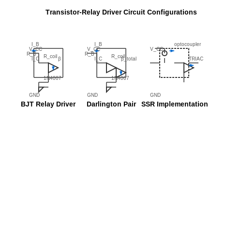
In a touch-activated light circuit, the transistor acts as an electronic switch, amplifying the weak current from the touch sensor to drive a higher-power load. For optimal performance, the BJT must operate in either the cutoff or saturation region, avoiding the linear region to minimize power dissipation. The base current \(I_B\) determines the operating state:
where \(I_C\) is the collector current and \(\beta\) is the DC current gain. For a relay coil drawing 100 mA and a transistor with \(\beta = 100\), the minimum base current must exceed 1 mA. The base resistor \(R_B\) is calculated as:
where \(V_{BE}\) is typically 0.7 V for silicon transistors.
Relay Driver Circuit Design
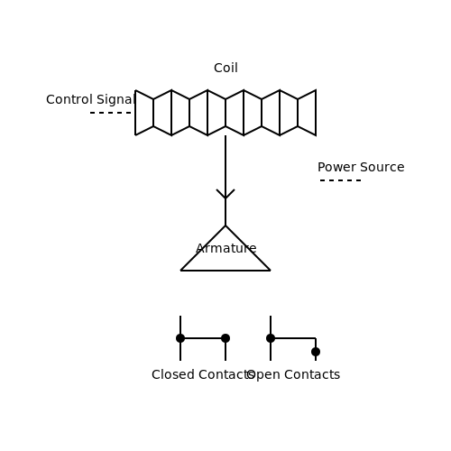
Electromechanical relays require a flyback diode to suppress voltage spikes caused by the collapse of the magnetic field when de-energized. The diode (e.g., 1N4007) must be placed in reverse bias across the relay coil. The relay's coil resistance \(R_{coil}\) determines the steady-state current:
For a 5 V relay with 100 Ω coil resistance, the current is 50 mA. The transistor must handle this current while maintaining saturation. Power dissipation in the transistor during conduction is:
where \(V_{CE(sat)}\) is typically 0.2 V for small-signal transistors like the 2N2222.
Darlington Pair for High-Gain Applications
When the touch sensor output current is exceptionally low (e.g., < 100 μA), a Darlington pair configuration provides sufficient gain. The composite current gain \(\beta_{total}\) is the product of individual transistor gains:
This configuration increases input impedance but introduces a higher \(V_{CE(sat)}\) (~1 V) due to the stacked base-emitter junctions.
Solid-State Relays (SSRs) as Alternatives
For silent operation and faster switching, SSRs use optocouplers and TRIACs/thyristors instead of mechanical contacts. Key parameters include:
- Isolation voltage: Typically 2.5–5 kV
- On-resistance: 50–100 mΩ for MOSFET-based SSRs
- Leakage current: < 1 mA in off-state
SSRs eliminate contact bounce but require heat sinks at higher currents due to \(I^2R\) losses.
2.3 Power Supply Considerations
The stability and efficiency of a touch-activated light circuit depend critically on the power supply design. Key parameters include voltage regulation, current capacity, noise immunity, and energy efficiency, each of which must be optimized for reliable operation.
Voltage Regulation Requirements
Touch sensors, particularly capacitive types, require a stable voltage supply to maintain consistent sensitivity. A voltage ripple exceeding 5% can lead to false triggering or reduced responsiveness. For a typical circuit operating at 3.3V or 5V, a low-dropout regulator (LDO) is often preferred over switching regulators due to its lower noise output. The power supply rejection ratio (PSRR) of the LDO should exceed 60 dB at frequencies below 1 MHz to attenuate noise from the input source.
where \( \Delta V_{\text{ripple}} \) is the peak-to-peak ripple voltage, \( I_{\text{load}} \) is the load current, \( f \) is the ripple frequency, and \( C_{\text{filter}} \) is the filter capacitance.
Current Capacity and Efficiency
The power supply must deliver sufficient current to drive the LED load while accounting for the touch sensor's quiescent current. For example, a circuit with a 20 mA LED and a touch IC drawing 1 mA requires a minimum current capacity of 21 mA. If battery-powered, the total energy budget \( E \) over time \( t \) is given by:
Lithium-ion batteries (3.7V) or AAA alkaline cells (1.5V) are common choices, with step-up converters used when higher voltages are needed. Efficiency \( \eta \) of the converter is critical:
Noise Mitigation Strategies
Capacitive touch circuits are susceptible to electromagnetic interference (EMI) and power supply noise. Decoupling capacitors (e.g., 100 nF ceramic) must be placed as close as possible to the touch IC's power pins. A pi-filter (LC or RC) can further suppress high-frequency noise:
For layouts with long power traces, a star grounding topology minimizes ground loops. Ferrite beads may be added in series with the power line to attenuate RF noise.
Case Study: Battery vs. USB Power
In a comparative analysis, a USB-powered touch light exhibited 2% lower false-trigger rates than a battery-powered version due to the USB host's inherent regulation. However, battery-powered designs achieved 30% longer lifetimes when paired with a duty-cycled touch IC (e.g., 1 ms active, 999 ms sleep).
LED or Bulb Selection
Key Parameters for Light Source Selection
The choice between LEDs and incandescent bulbs in a touch-activated light circuit depends on several critical factors, including power efficiency, luminous efficacy, spectral characteristics, and thermal management. For advanced applications, the following parameters must be rigorously evaluated:
- Forward Voltage (Vf) — Determines the minimum voltage required to activate the light source. LEDs typically operate between 1.8V (red) and 3.6V (blue/white), while incandescent bulbs require higher voltages, often 12V or more.
- Luminous Flux (Φv) — Measured in lumens (lm), this quantifies perceived brightness. High-power LEDs (e.g., Cree XLamp XHP70.2) achieve >4000 lm, whereas a 60W incandescent bulb emits ≈800 lm.
- Color Rendering Index (CRI) — Critical for applications requiring accurate color representation. LEDs with CRI >90 (e.g., Nichia Optisolis) outperform incandescent bulbs (CRI=100) in efficiency while maintaining high fidelity.
- Thermal Resistance (RθJA) — Impacts heat dissipation. LEDs require heatsinks for RθJA <10°C/W at >3W power, whereas incandescent bulbs radiate heat inefficiently (≈95% of energy as IR).
Mathematical Modeling of Efficiency
The wall-plug efficiency (η) of a light source is given by the ratio of luminous flux to input power:
For an LED driven at If=350 mA with Vf=3.2V and Φv=120 lm:
Comparatively, a 40W incandescent bulb with Φv=450 lm yields:
Drive Circuit Implications
LEDs necessitate constant-current drivers to prevent thermal runaway, governed by the diode equation:
where Is is reverse saturation current (≈10-12 A for Si), n is ideality factor (1.5-2.5 for LEDs), and VT=kT/q (25.85 mV at 300K). In contrast, incandescent bulbs present resistive loads (Rfilament ≈ V2/P), simplifying drive requirements but increasing I2R losses.
Advanced Considerations
- Flicker Performance — LEDs exhibit minimal persistence (τ≈10 ns), requiring PWM frequencies >400 Hz to avoid perceptible flicker. Incandescent bulbs have thermal inertia (τ≈100 ms), naturally suppressing flicker.
- EMI Characteristics — Fast-switching LED drivers generate high di/dt, necessitating LC filters. Incandescent circuits are inherently low-noise but radiate broadband thermal noise.
- Lifetime (L70) — High-quality LEDs maintain 70% initial flux for >50,000 hours (L70), whereas incandescent bulbs typically fail at 1,000-2,000 hours due to filament evaporation.
3. Basic Circuit Diagram
3.1 Basic Circuit Diagram
The touch-activated light circuit operates on the principle of capacitive sensing, where a conductive touch plate acts as one plate of a capacitor, and the user's finger introduces a detectable change in capacitance. The core circuit consists of a high-impedance input stage, a signal conditioning network, and a switching mechanism to control the light source.
Key Components and Their Roles
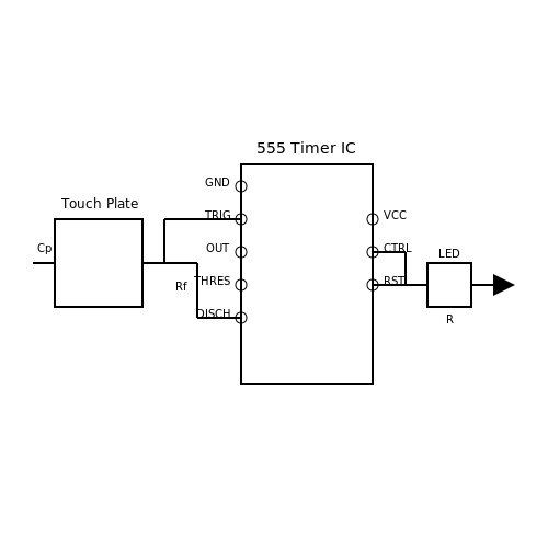
- Touch Sensor Plate: A conductive surface (e.g., copper pad) that forms a parasitic capacitance (Cp) with ground. Finger proximity increases this capacitance.
- High-Impedance Buffer: Typically an operational amplifier (op-amp) in a voltage follower configuration to prevent loading effects on the touch sensor.
- Signal Conditioning: An RC network or Schmitt trigger to convert the analog capacitance change into a digital signal.
- Switching Element: A transistor (BJT or MOSFET) or relay toggles the light source based on the processed signal.
Mathematical Analysis of Touch Sensitivity
The touch plate's capacitance without finger interaction is given by:
where ε0 is the permittivity of free space, εr is the relative permittivity of the substrate, A is the plate area, and d is the separation from ground. Finger contact introduces an additional capacitance ΔC in parallel:
Circuit Implementation
The schematic comprises:
- A 555 timer IC configured in monostable mode, triggered by the touch-induced capacitance change.
- A feedback resistor (Rf) setting the discharge time constant τ = RfCtotal.
- An LED driver stage with a current-limiting resistor to prevent overloading the output pin.
Practical Considerations
For reliable operation:
- The touch plate must be insulated to prevent DC contact, typically with a thin dielectric coating (e.g., acrylic).
- Noise immunity is enhanced by shielding the sensor traces and using a low-pass filter (R = 1 MΩ, C = 100 pF) at the input.
- Power supply decoupling (0.1 μF ceramic capacitor near the IC) minimizes false triggering.
Performance Optimization
The trigger threshold voltage Vth for the 555 timer is derived from the RC time constant:
where t is the charging time. For a detectable trigger, ΔC must cause a ≥10% shift in Vth relative to the untouched state.
3.2 Role of Each Component
Touch Sensor
The touch sensor acts as the input interface, detecting capacitive changes when a finger approaches or contacts the conductive surface. In advanced implementations, the sensor consists of a conductive pad connected to a high-impedance buffer. The human body introduces a parasitic capacitance Cp to ground, typically in the range of 1–10 pF. This capacitance forms part of an RC network whose time constant is disrupted by touch, generating a detectable signal.
where Rin is the input impedance of the buffer (often >1 MΩ) and Cstray represents board-level parasitic capacitance.
Signal Conditioning Circuit
Raw touch signals require amplification and noise filtering. A non-inverting operational amplifier configuration with a gain Av = 1 + (Rf/Ri) is typically employed. For high-frequency noise rejection, a low-pass filter with cutoff frequency fc is integrated:
Critical considerations include the amplifier's input bias current (preferably <100 pA for capacitive sensing) and power supply rejection ratio (PSRR) to mitigate supply noise.
Schmitt Trigger
This comparator with hysteresis converts the analog signal into a clean digital output, eliminating chatter. The threshold voltages VT+ and VT- are determined by:
where ΔV is the hysteresis window, typically 20–30% of Vcc for reliable switching. The Schmitt trigger's propagation delay (often <100 ns in CMOS implementations) must be compatible with the system's response time requirements.
Timer IC (555 or Modern Alternatives)
The monostable 555 configuration generates a fixed-duration pulse when triggered. The output pulse width tw is given by:
Advanced designs may substitute the 555 with microcontroller-based timers for programmable control. Key parameters include the timer's minimum trigger pulse width (often 100 ns–1 μs) and maximum duty cycle limitations.
Power MOSFET
This component switches the LED load with minimal voltage drop. The MOSFET's on-resistance RDS(on) determines power dissipation:
For high-current LEDs (>100 mA), gate charge (Qg) becomes critical—excessive charge can delay switching and increase losses. Modern logic-level MOSFETs with Qg < 10 nC are preferred.
LED and Current-Limiting Resistor
The resistor value is calculated based on the LED's forward voltage Vf and desired current ILED:
For high-efficiency designs, switching regulators may replace the resistor to minimize power loss. The LED's luminous intensity (in candela) and viewing angle must be matched to the application's requirements.
3.3 Voltage and Current Calculations
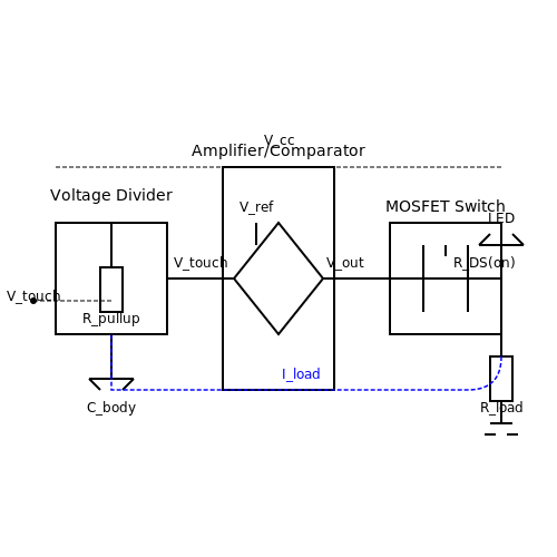
In a touch-activated light circuit, precise voltage and current calculations are essential to ensure proper operation of the sensing mechanism and the load. The circuit typically involves a high-impedance touch sensor, an amplifier or comparator stage, and a switching element (e.g., MOSFET or relay) to control the light.
Touch Sensor Voltage Divider
The touch sensor operates as a voltage divider, where human body capacitance (Cbody) forms the lower leg of the divider. The equivalent circuit can be modeled as:
where XCbody is the capacitive reactance of the human body interface:
Typical values for Cbody range from 1–100 pF, while Rpullup is usually in the range of 1–10 MΩ to maximize sensitivity.
Amplifier/Comparator Stage
The signal from the touch sensor is fed into an amplifier or comparator with a reference voltage (Vref). The output swings to the rail voltage when Vtouch crosses the threshold:
Switching Element Current
The load current (Iload) is determined by the power supply voltage and the load resistance (Rload), which could be an LED with a series resistor:
where Vf is the forward voltage drop of the LED. For a MOSFET-based switch, the gate drive current is negligible, but the drain current must be within the device's rated limits:
Power Dissipation
Power dissipation in the switching element must be calculated to avoid thermal overload. For a MOSFET in the on-state:
where RDS(on) is the drain-source on-resistance. Ensure Pdiss is below the device's maximum power rating at the operating temperature.
Practical Considerations
- Noise immunity: The high-impedance touch sensor is susceptible to electromagnetic interference. Shielding and proper PCB layout are critical.
- Leakage currents: High-value pullup resistors can introduce leakage paths. Use low-leakage components and clean PCB surfaces.
- Load transients: Inductive loads (e.g., relays) require flyback diodes to protect the switching element.
4. Soldering the Components
4.1 Soldering the Components
Thermodynamics of Soldering
Soldering relies on the principle of conductive heat transfer to form a metallurgical bond between components. The soldering iron tip, typically maintained at 300–400°C, transfers heat to the joint via conduction. The solder alloy (e.g., Sn60Pb40 or SAC305) undergoes a phase transition at its eutectic point, wetting the surfaces and forming an intermetallic compound (IMC) layer. The thermal equilibrium condition is governed by Fourier's law:
where T is temperature, t is time, and α is thermal diffusivity. For optimal joint formation, the heat input must exceed the solder's liquidus temperature (183°C for Sn63Pb37) but remain below the degradation threshold of PCB substrates (~250°C for FR-4).
Process Parameters and Optimization
Key variables affecting solder joint integrity include:
- Tip temperature: 315–370°C for leaded solder, 340–400°C for lead-free
- Dwell time: 1–3 seconds to prevent thermal damage
- Wetting angle: θ < 90° indicates proper metallurgical bonding
The intermetallic growth rate follows Arrhenius kinetics:
where x is IMC thickness, A is a pre-exponential factor, and Ea is activation energy (typically 0.4–1.2 eV for Cu-Sn systems).
Practical Techniques for Sensitive Components
When soldering the touch sensor's high-impedance nodes:
- Use low-thermal-mass tips (1–2 mm chisel) for precise heat control
- Apply no-clean flux to reduce oxidation without residue-induced leakage
- Implement thermal relief pads on ground planes to prevent heat sinking
For the MOSFET gate connections, limit soldering time to <2 seconds to prevent electrostatic discharge (ESD) damage. A grounded soldering iron with <20 mV tip potential is mandatory.
Quality Verification
Inspect joints under 10× magnification for:
- Concave fillet profile (contact angle 15–45°)
- Absence of dewetting (exposed base metal)
- Uniform intermetallic layer (1–5 µm thickness)
Measure joint resistance with a 4-wire ohmmeter; acceptable values are <50 mΩ for power connections and <1 Ω for signal paths. For the touch circuit, verify >1012 Ω insulation resistance between adjacent traces using a megohmmeter at 100 V DC.
Failure Modes and Mitigation
Common soldering defects in touch-sensitive circuits include:
- Cold joints: Characterized by grainy appearance; reflow with additional flux
- Whisker growth: Mitigate by using matte-finish solder and conformal coating
- Electromigration: Minimize with >0.5 mm trace spacing at touch nodes
Accelerated life testing at 85°C/85% RH for 1000 hours can predict long-term reliability. The touch circuit's solder joints should withstand >5000 thermal cycles between -40°C and 125°C without degradation.
4.2 Testing the Touch Sensor
Verifying Sensor Response Characteristics
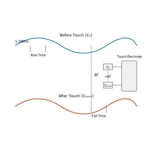
The touch sensor's performance depends critically on its capacitance change detection threshold. When a finger approaches the electrode, it introduces an additional capacitance Ctouch in parallel with the circuit's baseline capacitance C0. The total capacitance becomes:
For a typical RC oscillator-based touch sensor, the frequency shift Δf caused by Ctouch is given by:
Oscilloscope Measurement Protocol
Connect the probe to the sensor's output node while maintaining proper grounding. The expected waveform should show:
- Clear frequency modulation when touching the electrode
- Stable baseline oscillation (typically 1-10MHz range)
- Rise/fall times under 50ns for digital sensors
Quantitative Performance Metrics
Measure these key parameters with sub-millisecond resolution:
| Parameter | Acceptable Range | Measurement Method |
|---|---|---|
| Activation Threshold | 0.1-5pF | Capacitance meter in parallel |
| Response Time | <100ms | Digital storage scope |
| Hysteresis | <15% | Gradual approach/retract test |
Environmental Stability Testing
Evaluate performance under varying conditions:
- Humidity (30-90% RH)
- Temperature (0-50°C)
- EMI (0.1-1V/m RF fields)
The sensor should maintain consistent activation thresholds with less than ±10% variation across the specified operating range.
Failure Mode Analysis
Common issues and their root causes:
- False triggers: Insufficient shielding or improper grounding
- No response: Broken electrode connection or incorrect biasing
- Inconsistent activation: Poor RC time constant matching
4.3 Connecting the Load
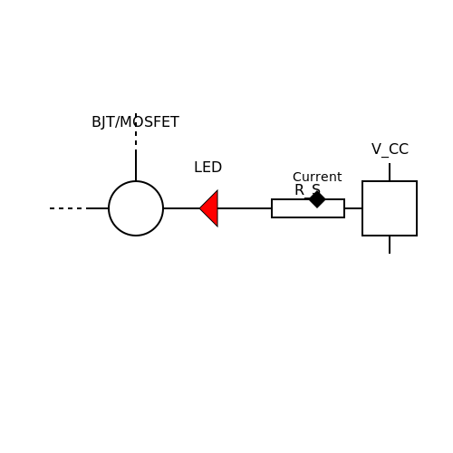
The load in a touch-activated light circuit typically consists of an LED or a low-power lamp, driven by the output stage of the circuit. The connection must account for voltage, current, and transient protection to ensure reliable operation. Below, we analyze the critical considerations for interfacing the load with the driving transistor or MOSFET.
Current and Voltage Requirements
The load current IL must not exceed the maximum current rating of the driving transistor or MOSFET. For an LED load, the forward current IF is governed by:
where VF is the LED forward voltage and RS is the current-limiting resistor. For incandescent lamps, the inrush current during turn-on must be mitigated using a negative temperature coefficient (NTC) thermistor or a soft-start circuit.
Transistor Switching Dynamics
When using a bipolar junction transistor (BJT) as a switch, ensure operation in the saturation region to minimize power dissipation:
where IB is the base current, IC is the collector current, and βsat is the forced beta. For MOSFETs, the gate drive voltage must exceed the threshold voltage VGS(th) to ensure low RDS(on).
Transient Protection
Inductive loads (e.g., relays) require a flyback diode to suppress voltage spikes during turn-off. The diode’s reverse breakdown voltage VRRM must exceed the supply voltage, and its forward current rating should match the load current. For capacitive loads, a series resistor may be needed to limit inrush current.
Practical Implementation
For an LED load, connect the anode to VCC via RS and the cathode to the transistor’s collector (for NPN) or drain (for N-channel MOSFET). For high-power loads, opt for a logic-level MOSFET with low RDS(on) to minimize conduction losses. Always verify thermal performance under continuous operation.
5. Sensor Not Responding
5.1 Sensor Not Responding
Common Causes and Diagnostics
When a touch-activated light circuit fails to respond, the issue often stems from one of three primary failure modes:
- Capacitive coupling degradation - The sensor plate loses proper coupling to ground
- Oscillator circuit failure - The feedback network sustaining oscillations becomes unstable
- Signal conditioning faults - Subsequent amplification or filtering stages distort the touch signal
The system's transfer function provides insight into expected behavior. For a basic RC touch sensor:
where R represents the equivalent resistance of the touch path and C the sensing capacitance. A non-responsive sensor typically shows either:
Oscillator Stability Analysis
For circuits using a 555 timer or Schmitt trigger oscillator, the Barkhausen criteria must be satisfied:
Common failure points include:
- Feedback resistor drift beyond 10% tolerance
- Parasitic capacitance exceeding 20pF at the sensing node
- Power supply ripple inducing phase noise
Practical Troubleshooting Steps
Follow this measurement sequence with a 100MHz oscilloscope:
- Verify 5V rail integrity (≤50mVpp ripple)
- Check for 1-10kHz oscillations at the sensor node
- Measure touch-induced frequency shift (Δf ≥ 5% expected)
- Confirm comparator hysteresis window (typically 100-300mV)
For differential capacitive sensors, the rejection ratio should exceed:
Advanced Debugging Techniques
When basic checks prove inconclusive, employ:
- Network analysis - Sweep 1kHz-1MHz to identify parasitic resonances
- Time-domain reflectometry - Locate impedance discontinuities in sensor traces
- Noise floor measurement - Ensure SNR > 20dB at the detection stage
The sensor's noise equivalent capacitance (NEC) provides a sensitivity benchmark:
where S is the sensitivity in V/pF. Modern touch ICs achieve NEC < 5fF.
5.2 Flickering Light Output
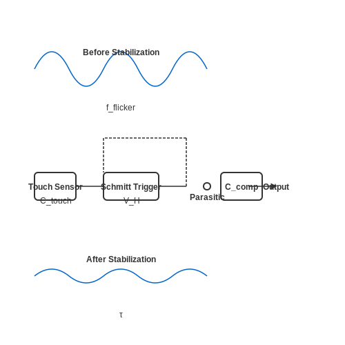
Flickering in a touch-activated light circuit typically arises from unstable triggering, power supply noise, or improper RC timing. For advanced designs, the root cause often lies in the time constant mismatch between the touch sensor's response and the load driver's switching characteristics.
Mathematical Analysis of Flicker Frequency
The flicker rate fflicker can be modeled as an underdamped oscillation in the feedback loop. Consider a touch sensor with capacitance Ctouch and a Schmitt trigger with hysteresis voltage VH:
where VT+ and VT- are the positive/negative threshold voltages. When the circuit's natural frequency fn approaches the Nyquist rate of the control loop:
Stabilization Techniques
Three primary methods suppress flicker in high-sensitivity circuits:
- Hysteresis Control: Increasing Schmitt trigger window VH beyond the noise floor (typically >100mV for 5V systems)
- Phase-Locking: Synchronizing the touch sampling rate with the AC mains frequency (50/60Hz) using a PLL
- Adaptive Filtering: Implementing a moving-average filter with time constant τ > 10/ftouch
Case Study: Capacitive Touch Flicker in LED Drivers
In a 12W LED driver using TTP223 touch ICs, flickering at 87Hz was traced to:
where Ileakage was 120nA through the ESD protection diode. The solution involved adding a 22pF compensation capacitor to alter the time constant:
Transient Response Optimization
For circuits using MOSFET drivers, the gate charge/discharge time must satisfy:
where fPWM is the dimming frequency. A common pitfall is neglecting the Miller plateau effect:
Using a gate driver with at least 2A peak current typically resolves this issue for power LEDs.
5.3 Overheating Components
Overheating in touch-activated light circuits primarily arises from excessive power dissipation in active components such as transistors, voltage regulators, or touch sensor ICs. The root cause often traces back to inadequate heat sinking, improper current handling, or suboptimal circuit design. Thermal runaway, where increased temperature further exacerbates power dissipation, poses a significant risk in poorly designed systems.
Thermal Dynamics in Semiconductor Components
The power dissipation PD in a bipolar junction transistor (BJT) or MOSFET driving the light load follows:
where VCE(sat) is the collector-emitter saturation voltage and RDS(on) the drain-source on-resistance. For example, a BJT with IC = 100 mA and VCE(sat) = 0.2 V dissipates 20 mW, while a MOSFET with RDS(on) = 0.5 Ω at the same current dissipates 5 mW. Despite lower dissipation, MOSFETs may still overheat due to:
- Insufficient copper area on PCB for heat dissipation
- Inadequate air flow in enclosed designs
- High ambient temperature exceeding component ratings
Thermal Resistance Analysis
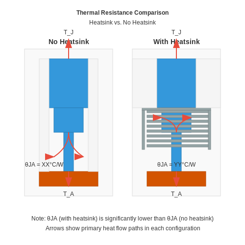
The junction temperature TJ depends on the thermal resistance θJA (junction-to-ambient) and power dissipation:
For a TO-92 package with θJA = 200°C/W dissipating 150 mW in a 25°C environment, TJ reaches 55°C. Exceeding the maximum junction temperature (typically 150°C for silicon devices) accelerates failure mechanisms like electromigration.
Mitigation Strategies
Effective thermal management techniques include:
- Heat sinking: Attaching a heatsink reduces θJA significantly. For example, a TO-220 package's θJA drops from 62°C/W to 35°C/W with a modest heatsink.
- Current derating: Operating components at 50-75% of maximum current ratings provides margin for thermal fluctuations.
- PCB layout: Increasing copper pour area under power components improves heat dissipation. A 1 oz copper plane measuring 1 in² provides approximately 45°C/W thermal resistance.
Case Study: Thermal Camera Analysis
Infrared imaging of a touch circuit prototype revealed localized heating near the voltage regulator (LM7805) reaching 78°C during continuous operation. The thermal profile showed:
- Regulator case temperature: 78°C
- Adjacent capacitor temperatures: 52°C
- Touch sensor IC temperature: 41°C
Adding a 10 cm² copper plane beneath the regulator reduced its temperature to 63°C, demonstrating the effectiveness of PCB-level heat spreading.
6. Adding a Dimmer Function
6.1 Adding a Dimmer Function
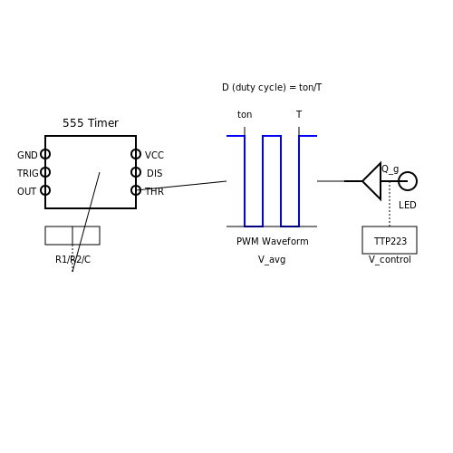
To introduce dimming capability into a touch-activated light circuit, a pulse-width modulation (PWM) approach is most effective. PWM allows precise control over the average power delivered to the load by varying the duty cycle of a high-frequency square wave. The duty cycle D is defined as the ratio of the ON time to the total period:
where ton is the ON time and T is the total period. The average voltage Vavg delivered to the load is then:
PWM Generation Using a 555 Timer
A 555 timer configured in astable mode can generate the necessary PWM signal. The frequency f and duty cycle are determined by resistors R1, R2, and capacitor C:
To enable adjustable dimming, replace R2 with a potentiometer. This allows manual control of the duty cycle while maintaining a fixed frequency (typically above 100 Hz to avoid visible flicker).
MOSFET Gate Drive Considerations
Since the 555 timer's output current is limited, a MOSFET driver (e.g., TC4427) or a bipolar transistor (e.g., 2N3904) may be required to drive high-power LEDs or incandescent bulbs. The gate charge Qg of the MOSFET determines the required drive current:
For fast switching and minimal power dissipation, ensure the gate driver can supply sufficient current to charge/discharge the MOSFET's gate capacitance within a small fraction of the PWM period.
Touch Interface Integration
To combine touch control with dimming, the touch sensor (e.g., a TTP223 IC) can modulate the 555 timer's control voltage (pin 5). Alternatively, a microcontroller (e.g., ATtiny85) can generate PWM directly while processing touch inputs for dynamic brightness adjustment. The touch sensor's output can be fed into an RC filter to produce an analog voltage for duty cycle control:
where t is the duration of touch activation. This voltage can then set the PWM duty cycle proportionally.
Practical Implementation Notes
- Frequency selection: For LED dimming, frequencies between 200 Hz and 1 kHz are optimal to avoid audible coil whine in driver inductors while eliminating visible flicker.
- EMI mitigation: High-frequency PWM can introduce electromagnetic interference; a small ferrite bead or LC filter on the output may be necessary.
- Thermal management: MOSFETs operating in linear mode (during transitions) must be heatsinked if the load current exceeds 500 mA.
6.2 Integrating with Smart Home Systems
Modern smart home ecosystems rely on standardized communication protocols to enable interoperability between devices. Integrating a touch-activated light circuit into such systems requires interfacing with these protocols, typically through a microcontroller or dedicated gateway.
Protocol Considerations
The dominant wireless protocols in smart home integration are Zigbee, Z-Wave, Wi-Fi, and Bluetooth Low Energy (BLE). Each has distinct advantages:
- Zigbee: Low-power, mesh networking at 2.4 GHz with ~100m range
- Z-Wave: Sub-GHz operation (better penetration) with 4-hop mesh capability
- Wi-Fi: High bandwidth but increased power consumption
- BLE: Optimized for intermittent, low-data-rate communication
The choice depends on power constraints, required responsiveness, and existing infrastructure. For battery-powered touch lights, Zigbee or BLE are typically optimal.
Gateway Interface Design
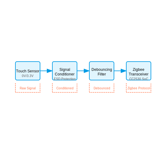
The touch sensor's output must be conditioned for smart home protocols. A typical implementation uses:
This digital signal feeds into a protocol-specific transceiver IC. For Zigbee, the CC2530 SoC provides both the 8051 microcontroller and 2.4GHz RF frontend. The signal conditioning circuit must account for:
- Voltage level shifting (if the touch IC operates at different logic levels)
- Debouncing (typically 10-50ms filter for mechanical touch sensors)
- ESD protection (IEC 61000-4-2 Level 4 compliance recommended)
Network Join Procedure
Commissioning the device into a smart home network involves cryptographic key exchange. For Zigbee 3.0, the process uses:
Where the install code is a 16-byte value printed on the device. The derived key authenticates the joining device through the following sequence:
- Trust center sends network key encrypted with $$K_{master}$$
- Device acknowledges with MIC (Message Integrity Code)
- Trust center issues unique 16-bit network address
Power Management
For battery-operated installations, power consumption must be minimized. The average current $$I_{avg}$$ can be estimated as:
Where typical values might be:
- $$I_{active}$$ = 15mA (RF transmission)
- $$I_{sleep}$$ = 1μA (deep sleep mode)
- $$t_{active}$$ = 5ms (per transmission)
- $$t_{sleep}$$ = 1s (between status updates)
This yields $$I_{avg} \approx 75μA$$, enabling multi-year operation on a 2000mAh coin cell.
Cloud Integration
For remote access, the gateway must bridge between local protocols and IP networks. MQTT is commonly used with payloads like:
{
  "device": "touch_light_01",
  "state": "on",
  "timestamp": 1634567890,
  "voltage": 3.1
}
The message broker (e.g., Mosquitto) routes these to home automation platforms like Home Assistant or OpenHAB through TLS-secured channels.
7. Recommended Books and Articles
7.1 Recommended Books and Articles
- PDF Seventh Edition Electronic Devices and Circuit Theory — 1.5 Extrinsic Materials—n- and p-Type 7 1.6 Semiconductor Diode 10 1.7 Resistance Levels 17 1.8 Diode Equivalent Circuits 24 1.9 Diode Specification Sheets 27 1.10 Transition and Diffusion Capacitance 31 1.11 Reverse Recovery Time 32 1.12 Semiconductor Diode Notation 32 1.13 Diode Testing 33 1.14 Zener Diodes 35 1.15 Light-Emitting Diodes ...
- Electrical and Electronic Devices, Circuits, and Materials ... — The increasing demand for electronic devices for private and industrial purposes lead designers and researchers to explore new electronic devices and circuits that can perform several tasks efficiently with low IC area and low power consumption. In addition, the increasing demand for portable devices intensifies the call from industry to design sensor elements, an efficient storage cell, and ...
- Practical Electronics for Inventors, Fourth Edition, 4th Edition — CHAPTER 7 Hands-on Electronics 7.1 Safety 7.1.1 Lecture on Safety Probably the most hazardous thing in electronics is your household line voltage, around 120 V at 60 Hz in the … - Selection from Practical Electronics for Inventors, Fourth Edition, 4th Edition [Book]
- PDF Mitchell A. Thornton, Fundamentals of Electronics Fundamentals of ... — Book 1: Electronic Devices and Circuit Applications Thomas F. Schubert, Jr. and Ernest M. Kim, University of San Diego This book, Electronic Devices and Circuit Application, is the first of four books of a larger work, Funda-mentals of Electronics. It is comprised of four chapters describing the basic operation of each of the four
- PDF AN11157 Capacitive touch sensing with high EMC performance — There are four important features of NXP's touch sensor family which provides one of the highest immunity sensor circuits on the market. 1. Wide input capacitance range: The steady state input capacitance on the sensor input is allowed to be in the range of 10 pF to 40 pF (60 pF for PCF8883 and PCF8886) without affecting the sensitivity. 2.
- PDF Fundamentals of Electronic Circuit Design - University of Cambridge — 7 1 The Basics 1.1 Voltage and Current Voltage is the difference in electrical potential between two points in space. It is a measure of the amount of energy gained or lost by moving a unit of positive charge ... In an electronic circuit, the electromagnetic problem of currents is typically
- Practical Electronics for Optical Design and Engineering — The next seven chapters introduce electronic devices of interest to optical engineers and build on the earlier chapters. Examples are provided throughout the book that range from simple calculations to sample MATLAB ® scripts. The aim of the MATLAB-based examples is to support an understanding of the fundamentals and relationships behind the ...
- PDF Fundamentals of Layout Design for Electronic Circuits — This book is able to connect the theoretical world of design automation to the practical world of the electronic-circuit layout generation. The text focuses on the physical/layout design of integrated circuits (ICs), but also covers printed circuit boards (PCBs) where needed. It takes the reader through a journey starting with
- (PDF) Advanced Practical Electronics - Circuits & Systems - ResearchGate — The first chapter is Introduction to Electronic Systems; Chapter 2 is on Power Supplies (using linear 7 switching regulators); Chapter 3 is on Power Devices; Chapter 4 is on the Theory of ...
- The Best Online Library of Electrical Engineering Textbooks — This book is intended to serve as a primary textbook for a one-semester introductory course in undergraduate engineering electromagnetics, including the following topics: electric and magnetic fields; electromagnetic properties of materials; electromagnetic waves; and devices that operate according to associated electromagnetic principles including resistors, capacitors, inductors ...
7.2 Online Resources and Tutorials
- design and construction of a touch activated alarm — Touch activated alarm is an electronic device that can be used as a security device. It is an electronic watch dog, because when installed to a door, and somebody touches the door, it sounds an alarm. ... 2.5 The Touch Point Unit - - - - - - 7 2.6 The Monostable Multivibrator Unit - - - 8 ... The objective is to construction ...
- Practical Troubleshooting of Electronic Circuits for Engineers and ... — Electronic Circuit Diagram . The Making of an Electronic Circuit. An electronic circuit makes use of both active and passive components. These components are physically interconnected with each other to form any electronic circuit. There are three major techniques to interconnect the components. Let us have a brief overlook of these methods ...
- Introduction to Electronics - Coursera — Resources • 10 minutes; Get ... Problem 7-2-2 • 30 minutes; Problem ... Be the end of the course you would definitely get confidence with the basics of electronics and once complicated circuits would look so easy to unravel. J. JG. 5. Reviewed on Sep 2, 2024. Amazing course. I had I great time solving the challenging problems; It is ...
- PCB Design and Circuit Simulator Software - Proteus — Proteus Design Suite is found in High Schools, Colleges and Universities across the world, teaching electronics, embedded design and PCB layout to tens of thousands of students each year. Circuit simulation gives students a fast and fun practical learning tool. A software solution allows instructors to prepare and re-use virtual labs.
- Table of Contents | Ultimate Electronics Book — Why this is a free, interactive electronics book. 0.1 Introduction 0.2 Schematics & Simulations Tutorial 1. Conceptual Foundations of Engineering. Powerful systems-level problem solving tools for electronics and beyond. 1.1 Algebraic Approximations 1.2 Orders of Magnitude, Logarithmic Scales, and Decibels 1.3 Complex Numbers
- PDF Fundamentals of Electronic Circuit Design - University of Cambridge — In an electronic circuit, the electromagnetic problem of voltages at arbitrary points in space is typically simplified to voltages between nodes of circuit components such as resistors, capacitors, and transistors. Figure 1.1: Voltage V1 is the electrical potential gained by moving charge Q1 in an electric field.
- Circuit Playground Express Workshop for Educators and Beginners — Welcome to the Circuit Playground Express Workshop! This workshop is geared toward educators and coding beginners, who want to get started programming with this easy to use platform. We will go over everything you need to know to get you started programming your Circuit Playground Express. We will focus on the educator friendly MakeCode programming interface. A little bit about me, my name is ...
- PDF Low-Power Touch Through Glass Reference Design - Texas Instruments — occupied by the microcontroller (MCU), light-emitting diode (LED), and passives in the printed circuit board (PCB). A medium-sized enclosure has an 8-cm glass window diameter and a four-button application. To account for the application requirements of this design, the TIDA-00343 has four buttons with 10-mm diameters.
- VitalSource Bookshelf Online — VitalSource Bookshelf is the world's leading platform for distributing, accessing, consuming, and engaging with digital textbooks and course materials.
- Home | Electronic Design — Articles, news, products, blogs and videos from undefined.
7.3 Datasheets for Components Used
- 7 Best Touch Sensor Switch Circuits Explored — In this post I have explained 8 easy methods of building touch sensor switch circuits at home, which can be used for switching 220 V appliances ON/OFF with ... Touch Switch light Circuits. Reply. Engr. Bash says. January 22, 2021 at 5:01 am ... Datasheets and Components (98) Electronics Theory (142) Free Energy (37) Games and Sports Projects (11)
- Touch Lamp Circuit using NE555 Timer — A touch lamp is a lamp that can be turned on and off by just touching a particular section of light. The electronic switch. Skip to content. About Us; Our Team ... This circuit can be used for a number of uses, such as an LED table, a reading lamp, and an LED lamp. It is also used for touch-activated portable emergency lights (If directly ...
- Types of Touch Switch Circuits Explained - Making Easy Circuits — In this post we discuss several different types of electronic touch switch circuit, which can be used to toggle an electrical load simply by touching a piece ... Light Activated Switch Circuit; 5. Radioactivity Detector Circuit; 6. Proximity Detector Circuit - LC Tuned IC CS209 ... Datasheets (10) DIY Projects (4) Electrical (15) Free Energy ...
- PDF Control Electronic Circuits With the Output of This Light Activated Switch — LIGHT ACTIVATED SWITCH CONTROL ELECTRONIC CIRCUITS WITH THE OUTPUT OF THIS ES SENTIAL INFORMATION BUILD INSTRUCTIONS CHECKING YOUR PCB & FAULT- FINDING ... Light Activated Before you start, take a look at the Printed Circuit Board (PCB). The components go in the side with the writing on and the solder goes on the side with the tracks and silver ...
- How to Build a Touch Sensor Circuit - Build Electronic Circuits — And you only need three components, how cool right? You can build this circuit if you're a total beginner. The Touch Sensor Circuit Diagram. You only need a resistor, a transistor, and an LED to build this project. Below you'll find the schematics for the touch sensor circuit: Components Needed. 9V Battery; 9V Battery Clip; Breadboard ...
- Digital Touch-Activated Switch Kit - PK025 - Etron Circuit Labs — Touch it on, touch it off. This Circuit will turn on the LED light with the touch of your finger and turn it off with a second touch. Full color instruction manual makes this kit easy to build while explaining the theory of operation. Kit includes all electronic components and the solderless prototype board needed for completion.
- Simple Touch Switch Circuit using 2n2222 Transistors — A 200KΩ variable resistor is used to adjust the sensitivity of the circuit. When you touch the touchpoints of the circuit a very small current starts passing through our skin which completes the circuit due to which both the transistors (Darlington pair) activate and the LED lights up. Applications and uses. Locks; Safety boxes; Lamps; Doors
- Electronics Datasheets - Parts Search and Technical Documents — Electronics Datasheets is a search engine containing over 9 million parts from thousands of manufacturers along with a comprehensive resource of datasheets and other technical documents. ... access to a comprehensive resource of datasheets and other technical documents from our growing database of electronics parts, sourced directly from the ...
- Datasheet Archive Search Engine — Datasheet Archive is a datasheet search engine with 500 million electronic ... The Datasheet Archive. The world's largest free resource for electronic component datasheets. Please enter a valid full or partial manufacturer part number with a minimum of 3 letters or numbers ... Over 16 years we have stored datasheets for over. 1 billion + parts ...
- Electronic Component Datasheets and Specifications - Mosaic Industries — Datasheets specifications for Power converters, Diodes, IGBTs, LED controllers/drivers, MOSFETs, Optocouplers, Embedded PCs, Processors, PWM Controllers, Sensors and sensor processing systems, Solar power converters, Transistors. Mosaic Documentation Web Providing Embedded Computers for Instruments & Automation ... Circuit protection components.