Electronic Structure of Semiconductor Materials
1. Definition and Basic Properties
Definition and Basic Properties
Semiconductor materials are crucial in modern electronics due to their unique electronic properties. Understanding their electronic structure is fundamental for engineers and researchers working in the semiconductor industry.
Band Structure
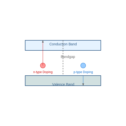
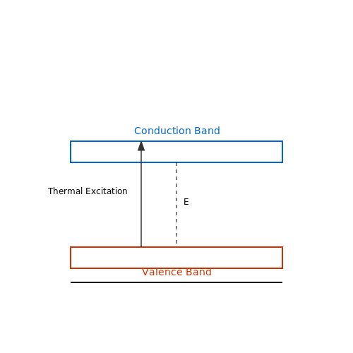
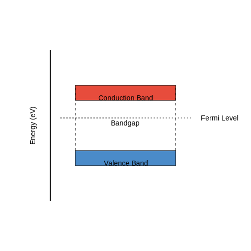
In semiconductors, the electronic structure is defined by the concept of band structure. This structure represents the energy levels that electrons can occupy within the material. The key feature of semiconductors is the presence of a bandgap, which separates the valence band (occupied energy states) from the conduction band (unoccupied energy states).
Doping
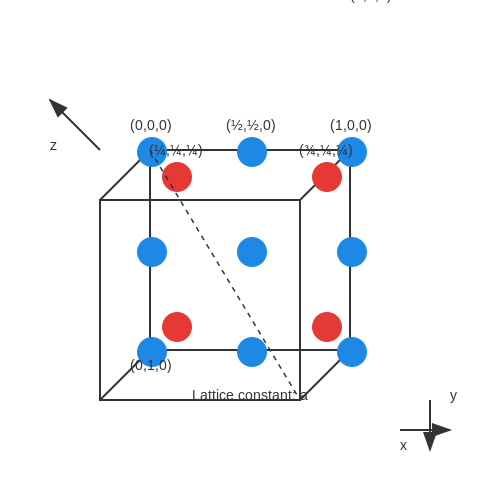
One of the defining characteristics of semiconductors is their ability to be doped with impurities, which significantly affects their conductivity. By introducing impurities into the crystal lattice, semiconductor properties can be tailored for specific applications.
Mobility and Carrier Concentration
The mobility of charge carriers (electrons or holes) and their concentration are vital parameters in semiconductor devices. Mobility describes how quickly charge carriers can move through the semiconductor material, while carrier concentration defines the number of charge carriers present.
Where:
- n is the electron concentration.
- n_i is the intrinsic carrier concentration.
- E_c is the energy level of the conduction band.
- E_f is the Fermi level.
- k is Boltzmann's constant.
- T is the temperature.
Real-World Applications
The knowledge of semiconductor electronic structure is applied in various technologies, such as integrated circuits, transistors, photovoltaic cells, and light-emitting diodes. By manipulating the electronic properties of semiconductors, engineers can design innovative devices for different industries.
Types of Semiconductors: Intrinsic and Extrinsic
Semiconductors are essential materials in electronic devices due to their unique electronic properties, particularly their conductivity between that of conductors and insulators. Semiconductors are broadly classified into two main types: intrinsic and extrinsic.Intrinsic Semiconductors
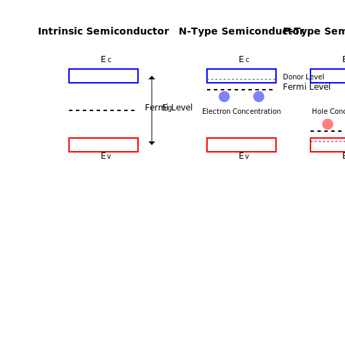
Intrinsic semiconductors are pure semiconducting materials like silicon (Si) and germanium (Ge) with no intentional impurities. These materials have their electrical conductivity primarily determined by thermal energy rather than impurities. In an intrinsic semiconductor, the number of thermally generated electrons in the conduction band is equal to the number of holes in the valence band, resulting in overall charge neutrality. Key points:- Intrinsic semiconductors have a narrow energy bandgap of around 1 eV, which allows for moderate conductivity at room temperature.
- Thermal excitation results in the generation of electron-hole pairs, contributing to the conductivity.
- The Fermi level lies near the middle of the bandgap in intrinsic semiconductors.
Extrinsic Semiconductors
Extrinsic semiconductors are doped semiconductors where small amounts of specific impurity atoms are intentionally added to the crystal lattice to modify its electrical properties. The two main types of extrinsic semiconductors are:N-type Semiconductors
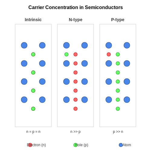
N-type semiconductors are doped with elements like phosphorus (P) or arsenic (As), which introduce extra electrons into the crystal structure. These impurity atoms have one more valence electron than the semiconductor material, leading to an excess of negative charge carriers (electrons) in the crystal. Key points:- N-type semiconductors have a higher electron concentration than hole concentration.
- Electron mobility is crucial in N-type semiconductors for efficient electronic device operation.
- Applications of N-type semiconductors include construction of transistors and diodes.
P-type Semiconductors
P-type semiconductors are doped with elements like boron (B) or indium (In), which introduce holes (deficient electron states) into the crystal lattice. These impurity atoms have one less valence electron than the semiconductor material, leading to an excess of positive charge carriers (holes) in the crystal. Key points:- P-type semiconductors have a higher hole concentration than electron concentration.
- Hole mobility is crucial in P-type semiconductors for efficient electronic device operation.
- Applications of P-type semiconductors include construction of transistors and diodes.
Band Theory and Energy Bands
In the realm of semiconductor materials, understanding the concept of energy bands and their behavior is crucial. Energy bands play a pivotal role in determining the electrical and optical properties of semiconductors.
Energy Bands in Solids
When multiple atoms come together to form a solid, their individual energy levels blend to create energy bands. The quantum nature of electrons leads to the formation of discrete energy levels within these bands.
The most significant energy bands in semiconductors are the valence band and the conduction band. The valence band contains the highest occupied electron energy levels at absolute zero temperature, while the conduction band holds vacant energy levels that electrons can move into under suitable conditions.
Band Gap
The separation between the valence band and the conduction band is referred to as the band gap. This band gap dictates several essential properties of the semiconductor, such as its conductivity, transparency, and ability to emit light when excited.
Energy Band Diagram
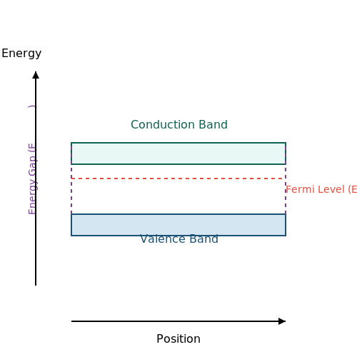
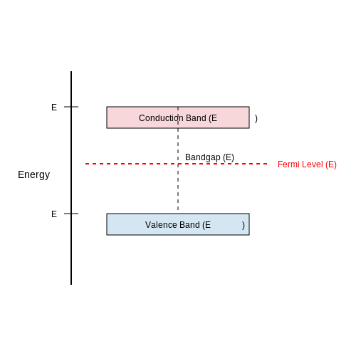
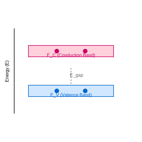
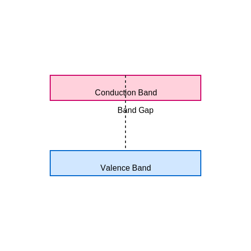
An energy band diagram is a graphical representation of the energy bands within a material. It visually illustrates the energy levels of electrons in both the valence and conduction bands, as well as the band gap between them.
Where:
- Egap is the band gap energy.
- EC is the energy of the conduction band.
- EV is the energy of the valence band.
Understanding the intricacies of energy band theory is fundamental in harnessing the full potential of semiconductor materials for various applications in electronics, optoelectronics, and beyond.
2. Electrons and Holes
2.2 Carrier Concentration and Doping
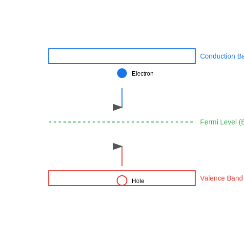
When dealing with semiconductor materials, understanding carrier concentration and doping is crucial. In semiconductors, the number of charge carriers—electrons and holes—greatly influences the material's conductivity and behavior. Carrier concentration refers to the density of these charge carriers within the material.
Carrier Concentration: The carrier concentration (n or p) in a semiconductor is determined by factors such as temperature, doping concentration, and bandgap energy. It can be mathematically expressed using equations derived from statistical mechanics and semiconductor physics.
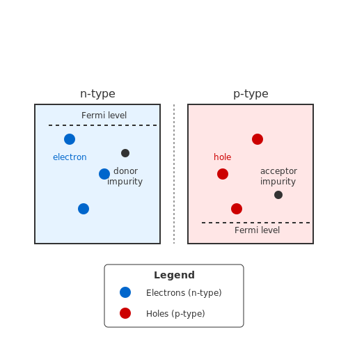
For an n-type semiconductor, the carrier concentration is primarily due to the excess electrons introduced by doping with donor impurities like phosphorus. In contrast, a p-type semiconductor has a higher concentration of holes resulting from acceptor impurities such as boron.
Doping: Doping is the intentional introduction of impurities into a semiconductor material to alter its electrical conductivity. By strategically adding donor or acceptor atoms, engineers can control the type and concentration of charge carriers, thus customizing the semiconductor's properties for specific applications.
Doping directly influences the concentration of free carriers in a semiconductor, shifting the Fermi level and affecting the material's conductivity. By modulating the doping levels, engineers can tune the semiconductor's characteristics, making it suitable for various electronic devices such as diodes, transistors, and integrated circuits.
2.3 Mobility and Conductivity
In semiconductor physics, mobility refers to the ability of charge carriers (electrons or holes) to move through the material under the influence of an electric field. It is a critical parameter that determines the conductivity of a semiconductor.
The mobility of charge carriers in a semiconductor can be mathematically expressed as:
where:
- μ is the mobility of the charge carrier
- q is the charge of the carrier
- τ is the carrier scattering time (mean time between scattering events)
- m is the carrier's effective mass
The mobility of electrons and holes in a semiconductor can vary based on factors like doping concentration, temperature, and crystal structure. In heavily doped semiconductors, where carrier concentrations are high, mobility is often lower due to increased scattering events.
Conductivity in semiconductors is a measure of how easily charge carriers can move through the material. It is given by:
where:
- n and p are the electron and hole densities
- μn and μp are the mobilities of electrons and holes respectively
High conductivity in semiconductors is crucial for the functioning of electronic devices as it allows efficient flow of current. Understanding the mobility and conductivity of semiconductors is fundamental for designing devices with optimal performance.
3. Fermi Level and Its Significance
Fermi Level and Its Significance
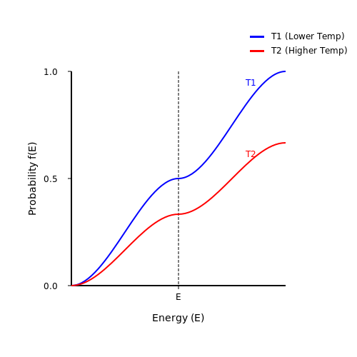
In semiconductor physics, the Fermi level plays a crucial role in understanding the electronic properties of materials. This concept is especially significant in advanced semiconductor devices and integrated circuits. The Fermi level represents the energy level at which the probability of finding an electron is 50%. The Fermi level influences various important phenomena in semiconductors, such as carrier concentration, conductivity, and energy band diagrams. It serves as a reference point for determining the distribution of electrons among energy levels in the semiconductor material. Key Points: - The Fermi level separates filled electronic states from empty states at absolute zero temperature. - Changes in the Fermi level affect the conductivity of a semiconductor. #### Understanding Fermi-Dirac Distribution Function The Fermi-Dirac distribution function describes the probability of finding an electron in an energy state at a given temperature. It takes into account the Pauli exclusion principle, which states that no two electrons can occupy the same quantum state simultaneously. The distribution function is given by:- Semiconductor Today — Stay updated with the latest advancements in semiconductor technology and industry trends.
- Nature - Semiconductors — Explore cutting-edge research articles on semiconductor materials and devices.
- Physica E: Low-dimensional Systems — Discover in-depth studies on low-dimensional semiconductor structures and their properties.
- MRS Bulletin — Access interdisciplinary research and reviews on materials science, including semiconductor advancements.
- ScienceDaily - Semiconductors — Read about the latest discoveries and breakthroughs in semiconductor research.
- Electronics Tutorials - Semiconductors — Explore detailed tutorials on semiconductor theory and applications.
- IEEE Transactions on Semiconductor Manufacturing — Access the latest research in semiconductor manufacturing processes and technologies.
3.2 Temperature Dependence of Semiconductor Properties
Semiconductor materials exhibit fascinating temperature-dependent behaviors that significantly impact their electronic properties. Understanding these variations is crucial for designing reliable electronic devices. ###Thermal Energy and Carrier Statistics
At higher temperatures, thermal energy disrupts the regular crystal lattice structure of semiconductors, increasing electron mobility due to higher kinetic energy. This phenomenon influences carrier statistics and conductivity. ###Bandgap Shrinking Effect
The semiconductor bandgap decreases with rising temperature due to thermal expansion leading to increased electron-hole pair generation. This effect alters the material's conductivity and optical properties, affecting device performance. ###Boltzmann Statistics and Carrier Concentrations
Utilizing Boltzmann statistics, the temperature dependence of carrier concentrations can be mathematically modeled. As temperature rises, more electrons transition from the valence to the conduction band, impacting the semiconductor's electrical behavior. ###Thermal Generation and Recombination Rates
Temperature influences the rate of thermal generation and recombination of electron-hole pairs in semiconductors. Optimal operating temperatures are critical to minimize these effects and enhance device efficiency. ###Impact on Semiconductor Device Performance
Understanding the temperature dependence of semiconductor properties is vital for optimizing device performance and reliability. Thermal considerations play a significant role in the design and operation of electronic systems.- Bandgap in Semiconductors — A comprehensive study on how the temperature impacts the bandgap in semiconductor materials and its implications on device performance.
- Temperature Effects on Semiconductors — An analysis of the temperature dependence of semiconductor properties and its relevance in electronic design.
- Semiconductor Physics and Band Theory — An educational resource exploring the fundamentals of semiconductor physics and band theory, including temperature effects.
- Temperature-Dependent Properties of Semiconductors — A detailed research article discussing the impact of temperature variations on semiconductor behavior and device performance.
3.3 PN Junctions and Diodes
In the world of semiconductor devices, the PN junction is a fundamental building block that underpins a plethora of electronic components. Understanding the behavior of PN junctions is crucial for designing and analyzing diodes, which are devices with unique electrical properties useful in various applications. ###PN Junctions: Unveiling the Boundaries
At the heart of a diode lies the PN junction, where a P-type (positive) semiconductor and an N-type (negative) semiconductor meet. This junction creates a depletion region, a space devoid of charge carriers that plays a pivotal role in the diode's functionality. The electric field across the depletion region establishes the diode's rectifying properties. ###The Diode Action: Harnessing the PN Junction
When a forward bias is applied to a diode, it allows current flow due to the reduction in the depletion region's width. In contrast, a reverse bias widens the depletion region, preventing significant current flow. This unidirectional conductance characterizes the essential rectifying function of diodes in electronic circuits. ###Understanding the Diode Equation
The behavior of a diode can be mathematically described by the Shockley diode equation:Applications in Electronics and Beyond
Diodes find extensive use in rectification, signal demodulation, voltage regulation, and oscillation generation in electronic circuits. Their simplicity and efficiency make them indispensable components across various industries, from power electronics to telecommunications. Embracing the complexities of PN junctions and diodes not only unlocks the secrets of electronic circuit design but also paves the way for innovative technological advancements. Mastering the interplay between semiconductor physics and device engineering is the cornerstone of modern electronic systems development.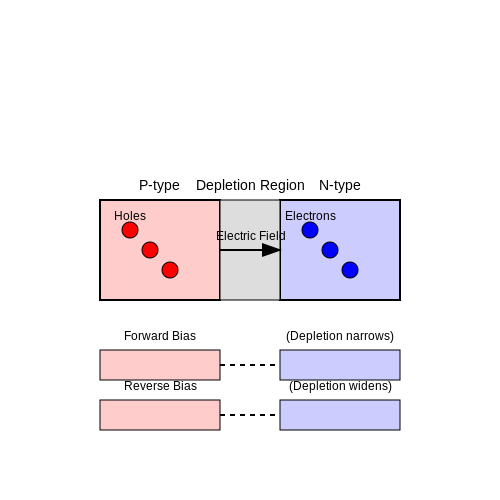
4. Transistors: BJT and FET
4.1 Transistors: BJT and FET
Transistors are fundamental components in modern electronics, serving as amplifiers and switches. Two common types are Bipolar Junction Transistors (BJT) and Field-Effect Transistors (FET). ## Bipolar Junction Transistors (BJT) BJTs consist of three regions: emitter, base, and collector. When a small current flows from the base-emitter junction, a larger current flows between the collector and emitter. This current amplification property makes BJTs ideal for applications requiring high current gain. ### Working Principle of BJT When a positive voltage is applied to the base relative to the emitter in an NPN transistor, it creates a forward bias on the base-emitter junction, allowing a current to flow from the emitter to the base. This current causes the collector current to flow, controlled by the base current. ### Equations for BJT The current-voltage relationship in a BJT can be described by the following equations: - Collector Current: $$I_C = \beta \cdot I_B$$ - Base-emitter Voltage: $$V_{BE} \approx 0.7$$ V (for silicon-based BJT) ## Field-Effect Transistors (FET) FETs are voltage-controlled devices with three terminals: gate, source, and drain. The FET's conductivity is determined by the voltage applied to the gate terminal, making it ideal for high impedance and low power applications. ### Types of FETs There are two main types of FETs: - MOSFET (Metal-Oxide-Semiconductor FET) - JFET (Junction FET) Each type has unique characteristics and applications based on their construction and behavior. ### MOSFET Working Principle In a MOSFET, applying a voltage to the gate terminal creates an electric field that modulates the conductivity between the source and drain terminals. This voltage-controlled behavior allows MOSFETs to operate over a wide range of frequencies. ### Equations for FET The operation of FETs can be mathematically described by the following equations, among others: - Drain Current (MOSFET): $$I_D = \mu_{n} \cdot C_{ox} \cdot \frac{W}{L} \cdot (V_{GS} - V_{TH})^2$$ --- Having a solid understanding of BJT and FET fundamentals is crucial for designing and optimizing electronic circuits, especially in high-frequency and high-power applications where these devices play a vital role. By mastering the principles behind these transistors, engineers can create efficient and reliable electronic systems tailored to specific needs and requirements.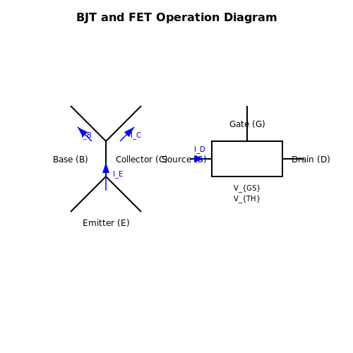
4.2 Photovoltaic Cells
In the realm of semiconductor materials, photovoltaic cells play a pivotal role in converting sunlight into electricity. Understanding the electronic structure behind their operation is essential for optimizing their efficiency and performance. Let's delve into the intricate workings of these devices. ###Semiconductor Band Structure in Photovoltaic Cells
Photovoltaic cells predominantly utilize semiconductor materials due to their unique electronic properties. These materials have a band structure comprising valence and conduction bands with a bandgap in between. When photons from sunlight strike the semiconductor, they generate electron-hole pairs, leading to an internal electric field within the cell. ###Working Principle of Photovoltaic Cells
1. Absorption: Sunlight containing photons is absorbed by the semiconductor material. 2. Generation: The absorbed energy excites electrons from the valence band to the conduction band, creating electron-hole pairs. 3. Separation: The internal electric field within the semiconductor separates the electrons and holes. 4. Collection: Electrons and holes are collected at the respective terminals, generating usable electrical power. ###Key Parameters for Photovoltaic Cell Efficiency
To assess the performance of photovoltaic cells, several key parameters are crucial: - Efficiency: The ratio of electrical energy generated to the incident solar power. - Fill Factor (FF): Represents how effectively the cell converts sunlight to electricity. - Open-Circuit Voltage (Voc): The maximum voltage across the cell under no load conditions. - Short-Circuit Current (Isc): The current produced when the cell is short-circuited. - Maximum Power Point (MPP): The operating point where the cell generates maximum power. ###Applications and Innovations
Photovoltaic cells find applications in various sectors, including residential, commercial, and industrial settings, contributing to clean energy generation. Recent advancements in materials science and device design have led to improvements in efficiency and durability, paving the way for solar-powered technologies in diverse fields. ###Quantum Efficiency and Spectral Response
Understanding the quantum efficiency and spectral response of photovoltaic cells is crucial for evaluating their performance across different wavelengths of sunlight. Quantum efficiency quantifies the ratio of electrons generated to incident photons, while spectral response indicates the cell's ability to convert specific wavelengths into electricity. ###Conclusion
Photovoltaic cells exemplify the synergy between semiconductor physics and renewable energy technology, offering a sustainable solution to energy generation. By enhancing our comprehension of the electronic structure governing their operation, we can advance the efficiency and effectiveness of solar energy systems, driving towards a cleaner and greener future.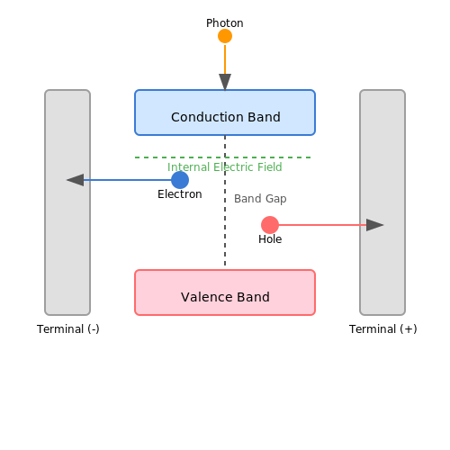
4.3 Light Emitting Diodes (LEDs)
In the intricate realm of semiconductor devices, Light Emitting Diodes (LEDs) hold a prominent position due to their distinctive property of converting electrical energy into visible light. Understanding the underlying principles governing the operation of LEDs is essential for a plethora of advanced applications in lighting, displays, optoelectronics, and communication systems. ###Operating Principle of LEDs
LEDs operate based on the phenomenon of electroluminescence, where carriers (electrons and holes) recombine in a semiconductor material, generating photons in the process. This emission of photons results in the characteristic light output from LEDs. The key components of LED structure include: - P-N Junction: A crucial element where electron-hole recombination occurs, leading to light emission. - Active Layer: The region within the semiconductor where carrier recombination and light generation predominantly take place. - Contact Layers: Facilitate the flow of electrons and holes into the active region. The process starts with the application of a forward bias to the p-n junction, allowing the injection of minority carriers (electrons into the p-region and holes into the n-region). As electrons recombine with holes at the junction, energy is released in the form of photons, creating the characteristic emission. ###Band Structure and Emission Wavelength
The bandgap energy of the semiconductor material determines the emitted wavelength of light. By tuning the bandgap energy through careful selection of material composition, it is possible to achieve specific colors of light emission. For instance, materials like Gallium Nitride (GaN) are utilized for blue LEDs, while Indium Gallium Nitride (InGaN) enables the production of green LEDs. ###Efficiency and Applications
LEDs are renowned for their high energy efficiency, durability, and longevity compared to traditional lighting sources. Due to their compact size and low power consumption, LEDs find extensive applications in: - Lighting Systems: Illumination for both residential and commercial settings. - Display Technologies: LED displays in televisions, monitors, and signage. - Optoelectronics: Optical communication systems and sensors. - Automotive Lighting: Headlights, tail lights, and interior lighting applications. The versatility and efficiency of LEDs continue to drive innovation in various industries, revolutionizing the way we perceive and utilize light. ###Mathematical Formulation
The efficiency of LEDs can be quantified through parameters such as external quantum efficiency, internal quantum efficiency, and radiative recombination rate. These metrics play a crucial role in determining the overall performance and efficacy of the LED device.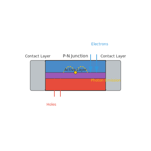
5. Semiconductors in Digital Electronics
5.1 Semiconductors in Digital Electronics
In the realm of digital electronics, semiconductors play a crucial role in shaping the landscape of modern technology. Understanding the electronic structure of semiconductor materials is fundamental for advanced-level professionals in disciplines such as engineering, physics, and research. Let's delve into the intricate workings of semiconductors in the context of digital electronics.
Semiconductor Basics
Before we explore the applications of semiconductors in digital electronics, let's revisit the foundational concepts concerning semiconductor materials. Semiconductors have an intermediate conductivity between insulators and conductors due to their partially filled valence bands.
Intrinsic vs. Extrinsic Semiconductors
Discussing the classification of semiconductors into intrinsic and extrinsic types is essential to comprehend their behavior in electronic devices. Intrinsic semiconductors consist of pure semiconductor materials, while extrinsic semiconductors are doped to modify their properties.
Band Theory and Energy Levels
Exploring the band theory of semiconductors aids in understanding their electronic structure. Valence bands and conduction bands, separated by the band gap, dictate the electrical properties of semiconductors and influence their behavior in digital circuits.
Semiconductor Physics in Digital Logic
Applying semiconductor physics to digital logic forms the backbone of modern computing systems. The manipulation of electron flow through semiconductors enables the creation of logic gates, essential components in digital circuits.
Real-World Applications
From integrated circuits to microprocessors, semiconductors power a myriad of digital devices that shape our daily lives. Understanding the electronic structure of semiconductors is pivotal for designing and optimizing these cutting-edge technologies.
Further Exploration
For advanced insights into semiconductor materials and their applications in digital electronics, delve deeper into the nuances of semiconductor behavior, quantum effects in nanoscale devices, and the future prospects of semiconductor technology.
---Explore the intricate world of semiconductors in digital electronics to unleash the full potential of modern technology.
5.2 Role of Semiconductors in Renewable Energy
Semiconductors play a vital role in the realm of renewable energy, acting as key components in various technologies that harness natural resources sustainably. Understanding the intricacies of how semiconductors interact with energy sources like sunlight or heat is crucial for maximizing efficiency and performance.
Solar Photovoltaics
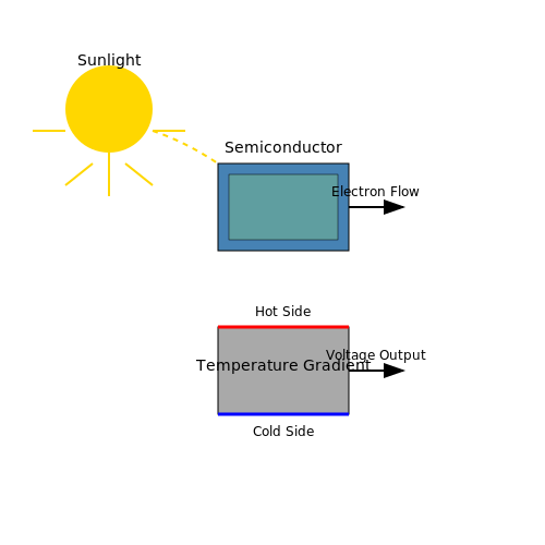
One of the most prominent applications of semiconductors in renewable energy is in solar photovoltaics. When light strikes a semiconductor material such as silicon, it excites electrons, creating a flow of current. This process forms the basis of solar panels, converting sunlight directly into electricity.
The bandgap of the semiconductor used in solar cells determines the efficiency of energy conversion. Tuning the bandgap allows for optimization of absorption across different parts of the solar spectrum, increasing overall energy output.
Thermoelectric Generators
Semiconductors are also crucial in thermoelectric generators, converting heat differentials into electricity. By exploiting the Seebeck effect, where a temperature gradient induces voltage, these generators offer a sustainable way to harness waste heat or geothermal energy.
Selecting appropriate semiconductor materials with the right thermoelectric properties is essential for optimizing efficiency. By improving the figure of merit through material engineering, researchers aim to enhance the performance of thermoelectric devices for broader applications.
Energy Storage
Semiconductor-based devices are pivotal in energy storage systems like batteries and supercapacitors. In these systems, semiconductors often serve as electrodes or as components within the energy storage mechanism, facilitating the transfer of charge and energy storage capabilities.
By developing new semiconductor materials with enhanced charge carrier mobility and stability, researchers aim to improve the storage capacity, efficiency, and lifespan of energy storage devices, thereby advancing the feasibility of renewable energy solutions.
---
Emerging Technologies in Semiconductor Materials
Advanced research in semiconductor materials has paved the way for the development of groundbreaking technologies with diverse applications. In this subsection, we explore some of the most exciting emerging technologies shaping the future of electronics and photonics.
The Role of Quantum Dots
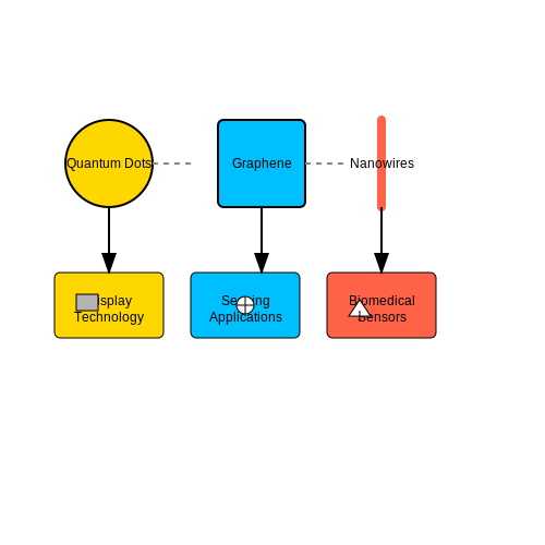
Quantum dots have gained significant attention for their potential in various applications, including displays, solar cells, and medical imaging. These nanoscale semiconductor particles exhibit unique electronic properties due to quantum confinement effects.
Applications in Display Technology
Quantum dots show promise in enhancing display technologies by enabling a wider color gamut and improved brightness levels. By efficiently converting blue light into red and green emissions, quantum dot displays offer vivid and lifelike colors.
2D Materials for Electronics
Atomically thin 2D materials such as graphene and transition metal dichalcogenides (TMDs) have revolutionized the field of electronics. With exceptional electronic properties, these materials hold the potential to enable ultrafast transistors, flexible devices, and efficient energy conversion systems.
Graphene Transistors
Graphene transistors have demonstrated exceptional electron mobility, making them ideal for high-speed electronic devices. The unique band structure of graphene allows for precise control of charge carriers, paving the way for next-generation electronics.
Nanowires for Sensing Applications
Nanowires offer a versatile platform for sensing applications due to their high surface-to-volume ratio and tunable properties. By functionalizing semiconductor nanowires, researchers have developed highly sensitive sensors for detecting gases, biomolecules, and environmental pollutants.
Biomedical Sensor Arrays
Integrated arrays of semiconductor nanowire sensors have shown great potential for biomedical applications, enabling the detection of specific biomarkers and pathogens in biological samples. These sensors offer rapid and sensitive detection capabilities for diagnostic purposes.
6. Recommended Textbooks
6.1 Recommended Textbooks
- Semiconductor Physics and Devices: Basic Principles - Donald A. Neamen — This textbook is an excellent resource for understanding the fundamental principles governing the electronic properties of semiconductor devices, including detailed semiconductor physics and the comprehensive study of the materials used in the industry.
- Solid State Physics - Neil W. Ashcroft, N. David Mermin — A classic reference in solid state physics, this book covers theoretical underpinnings necessary for graduate-level studies by exploring crystal structures, electronic properties, and collective phenomena in solids.
- Semiconductor Physics and Applications - M. Balkanski, R. F. Wallis — This book provides comprehensive coverage of the physics and properties of semiconductors with a balanced view of the quantum mechanical frameworks and practical applications, assisting engineers and physicists in both research and application.
- Electronic Materials Science - Eugene A. Irene — Especially useful for materials scientists and engineers, this book encompasses a wide range of topics, such as electrical characterization techniques, and offers insights into advanced semiconductor devices and their real-world implementations.
- Fundamentals of Semiconductors - Peter Y. Yu, Manuel Cardona — This book presents both basic and complex concepts involving semiconductor physics, from quantum mechanics and band structure analyses to the interactions between electrons and phonons, ideal for readers pursuing research.
- Principles of Semiconductor Devices and Heterojunctions - Bart Van Zeghbroeck — With a focus on device applications and heterojunction technologies, this textbook serves as a practical guide to the electronic properties of semiconductor devices and their influence on modern electronics.
- target="_blank" class="external" title="The Physics of Low-Dimensional Semiconductors"> The Physics of Low-Dimensional Semiconductors - John H. Davies — This resource is targeted at those interested in the unique properties and applications of low-dimensional semiconductor systems, such as quantum wells, wires, and dots.
6.2 Online Resources and Websites
- MIT OpenCourseWare - Electronic Structure of Materials — Offers comprehensive lecture notes and resources on the electronic structure of materials, ideal for deepening understanding of semiconductor materials at an academic level.
- Physical Review B - Condensed Matter and Materials Physics — This journal provides the latest research articles and papers on the condensed matter, including semiconductor materials and their electronic structures.
- Journal of Materials Research — Features peer-reviewed papers on innovative semiconductor materials and their characterization, including analysis of their electronic structure.
- nanoHUB.org - Simulation Tools — Offers advanced simulation tools for studying electronic structure and behavior of nanostructured materials, beneficial for practical applications in semiconductor research.
- Semiconductor Today — A reliable resource for the latest developments in the industry including research insights on advanced semiconductor materials and their electronic configurations.
- ResearchGate — An academic network platform that allows researchers to access and share papers, including those focusing on the electronic properties of semiconductor materials.
- Journal of Computational Electronics — Publishes articles on theoretical and computational methods for understanding electronic properties, offering significant insights into semiconductor electronic structures.
- arXiv.org - Condensed Matter — A vast repository of pre-publication articles, bringing the latest in condensed matter research including studies on the electronic structure of semiconductors.
- MDPI Electronics Journal — A peer-reviewed open-access journal that covers advanced topics in electronics and offers articles on the electronic structure research of semiconductor materials.
- npj Computational Materials — Provides cutting-edge research on computational predictions of electronic structures, which are crucial for designing new semiconductor materials.
6.3 Research Papers and Journals
- Semiconductor Science and Technology — A peer-reviewed journal that covers various aspects of semiconductor materials. It provides comprehensive insights into new developments and experimental findings in the field of semiconductors.
- Physical Review B - Semiconductors — This section of the Physical Review B journal focuses on research papers that delve into the electronic structure and properties of semiconductor materials, offering both theoretical and experimental perspectives.
- Progress in Solid State Chemistry — Hosted by Elsevier, this journal publishes articles that explore the chemical properties and electronic structure of semiconductor materials, emphasizing the progress in solid-state chemistry.
- Langmuir — A journal by the American Chemical Society, Langmuir focuses on the interface between molecular and surface materials, which includes extensive research on semiconductor materials and their electronic properties.
- Journal of Electronic Materials — Published by SAGE, this journal covers the peer-reviewed research related to materials used in electronics and optoelectronics, providing insights into the electronic structures of semiconductors.
- Advanced Materials — A leading journal providing interdisciplinary research articles on advanced semiconductor materials, their synthesis, properties, and practical applications in various technology sectors.
- Materials at the Nanometer Level — This journal specializes in the nanoscale characteristics of materials, offering valuable research on the nanostructured semiconductor materials and their electronic structures.