Semiconductor Basics
1. Definition and Basic Properties
Semiconductor Basics
1.1 Definition and Basic Properties
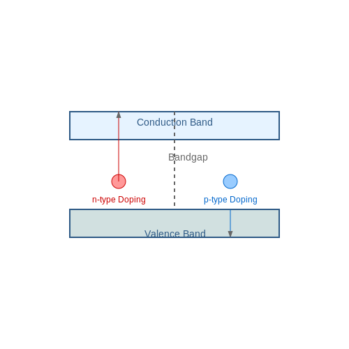
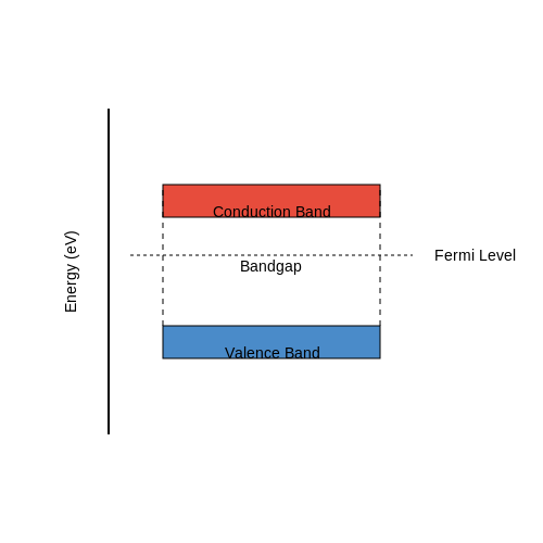
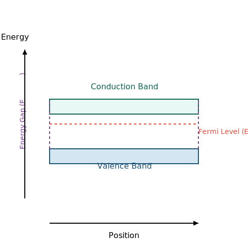
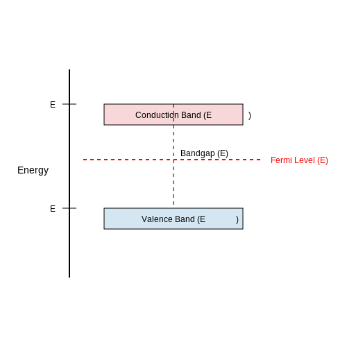
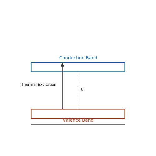
Semiconductors are materials with an electronic band structure where the valence band is fully occupied, and the conduction band is empty at absolute zero temperature. Their defining characteristic is an energy gap (bandgap, \(E_g\)) between the valence and conduction bands, typically ranging from 0.1 eV to 3.5 eV. This intermediate conductivity arises from their ability to be precisely doped with impurities, enabling controlled charge carrier modulation.
Band Theory and Charge Carriers
The electronic properties of semiconductors are governed by quantum mechanical band theory. At finite temperatures, thermal excitation promotes electrons from the valence band to the conduction band, leaving behind holes. The intrinsic carrier concentration (\(n_i\)) is derived from the Fermi-Dirac distribution and density of states:
where \(N_c\) and \(N_v\) are the effective densities of states in the conduction and valence bands, respectively, \(k\) is Boltzmann’s constant, and \(T\) is temperature. For silicon at 300 K, \(n_i \approx 1.5 \times 10^{10} \, \text{cm}^{-3}\).
Doping and Extrinsic Semiconductors
Doping introduces deliberate impurities to alter conductivity:
- n-type doping (e.g., phosphorus in silicon) adds donor electrons near the conduction band.
- p-type doping (e.g., boron in silicon) creates acceptor states near the valence band.
The majority carrier concentration in doped semiconductors follows:
where \(N_d\) and \(N_a\) are donor and acceptor densities. Minority carriers are suppressed but critical for device operation (e.g., diffusion currents in diodes).
Mobility and Conductivity
Charge transport is characterized by mobility (\(\mu\)), which quantifies how easily carriers move under an electric field. Conductivity (\(\sigma\)) combines carrier density and mobility:
where \(q\) is the elementary charge, and \(\mu_n\), \(\mu_p\) are electron and hole mobilities. In silicon, \(\mu_n \approx 1400 \, \text{cm}^2/\text{V}\cdot\text{s}\) and \(\mu_p \approx 450 \, \text{cm}^2/\text{V}\cdot\text{s}\) at 300 K, with strong temperature and doping dependence.
Temperature Dependence
Semiconductor behavior is highly temperature-sensitive:
- At low temperatures, carriers freeze out at dopant sites.
- Near room temperature, extrinsic conduction dominates.
- At high temperatures, intrinsic carriers overwhelm doping effects.
The bandgap also varies with temperature, often modeled by Varshni’s equation for materials like GaAs:
where \(\alpha\) and \(\beta\) are material-specific constants.
Practical Implications
These properties underpin semiconductor device design. For instance, the bandgap determines the spectral response of photodetectors, while doping profiles define transistor thresholds. Mobility impacts switching speeds in integrated circuits, and temperature stability is critical for power electronics.
1.2 Intrinsic vs. Extrinsic Semiconductors
Fundamental Definitions
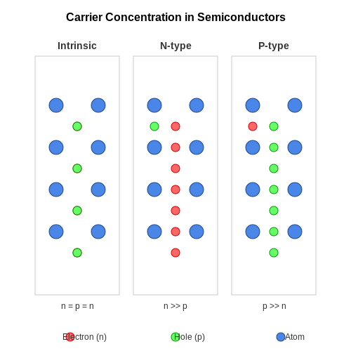
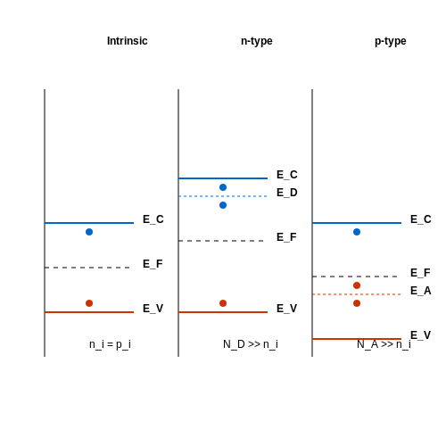
An intrinsic semiconductor is a pure crystalline material (typically silicon or germanium) where charge carrier concentration is determined solely by thermal excitation across the bandgap. The electron density n and hole density p are equal (n = p = ni), where ni is the intrinsic carrier concentration. This condition holds only when no dopants or impurities are present.
Here, Nc and Nv are the effective density of states in the conduction and valence bands respectively, Eg is the bandgap energy, k is Boltzmann's constant, and T is temperature.
Extrinsic Semiconductors: Doping Mechanisms
Extrinsic semiconductors are intentionally doped with impurities to modify their electrical properties. Two primary types exist:
- n-type: Doped with donor atoms (e.g., phosphorus in silicon) that introduce additional electrons into the conduction band. The majority carriers are electrons (n ≈ ND), where ND is the donor concentration.
- p-type: Doped with acceptor atoms (e.g., boron in silicon) that create holes in the valence band. The majority carriers are holes (p ≈ NA), where NA is the acceptor concentration.
Charge Neutrality Condition
In extrinsic semiconductors, the charge neutrality condition governs carrier concentrations:
Where NA- and ND+ represent ionized acceptor and donor densities. At room temperature, nearly all dopants are ionized (NA- ≈ NA, ND+ ≈ ND).
Temperature Dependence
The behavior of extrinsic semiconductors varies with temperature:
- Freeze-out region (low T): Dopants are not fully ionized. Carrier concentration follows an exponential activation law.
- Extrinsic region (room T): Dopants are fully ionized, and carrier concentration is approximately equal to the net doping (n ≈ ND - NA for n-type).
- Intrinsic region (high T): Thermal excitation dominates over doping effects, and the material behaves like an intrinsic semiconductor (n ≈ p ≈ ni).
Practical Implications
Extrinsic semiconductors form the basis of all modern electronic devices. Key applications include:
- pn junctions: Formed by adjacent p-type and n-type regions, enabling diodes and transistors.
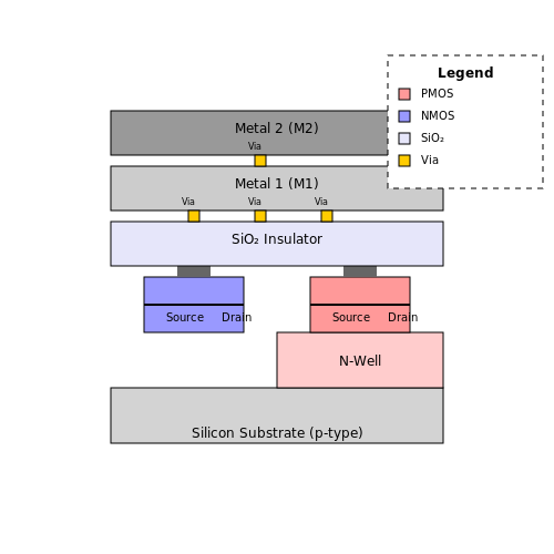
- CMOS technology: Utilizes complementary p-type and n-type MOSFETs for low-power logic circuits.
- Optoelectronics: Doping profiles control light emission in LEDs and laser diodes.
Mobility and Conductivity
The conductivity σ of a semiconductor depends on both carrier concentration and mobility:
Where μn and μp are electron and hole mobilities. In extrinsic materials, the majority carrier term dominates. Mobility decreases with increasing doping due to impurity scattering, creating a trade-off between carrier concentration and mobility in device design.
1.3 Band Theory and Energy Gaps
In crystalline solids, electron energy levels split into closely spaced states forming energy bands. The band theory explains the conductive properties of materials by analyzing the distribution of these electron states. The two most critical bands are the valence band (highest occupied electron states) and the conduction band (lowest unoccupied states). The energy difference between them is the band gap (Eg), a defining parameter for semiconductors and insulators.
Formation of Energy Bands
When atoms come together to form a crystal lattice, their discrete atomic orbitals overlap, creating a continuum of energy levels. For N atoms, each atomic state splits into N closely spaced molecular orbitals, forming an energy band. The width of the band depends on the strength of orbital overlap, with tightly bound inner electrons forming narrow bands and valence electrons forming broader bands.
where E(k) is the electron energy as a function of wave vector k, E0 is the atomic energy level, β represents the crystal field effect, γ is the overlap integral, and a is the lattice constant.
Band Gap and Material Classification
The band gap determines a material's electrical behavior:
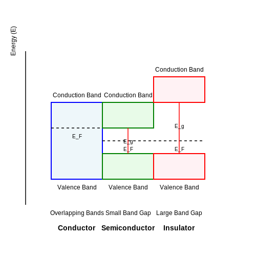
- Conductors: Valence and conduction bands overlap (Eg ≈ 0 eV), allowing free electron movement.
- Semiconductors: Small band gap (0.1–2.5 eV), enabling thermal or optical excitation of electrons.
- Insulators: Large band gap (>5 eV), preventing electron promotion under normal conditions.
Direct vs. Indirect Band Gaps
In direct band gap semiconductors (e.g., GaAs), the conduction band minimum and valence band maximum occur at the same k-vector, allowing efficient photon absorption/emission. In indirect band gap materials (e.g., Si, Ge), these extrema are misaligned, requiring phonon assistance for transitions—critical for optoelectronic device efficiency.
where α is the absorption coefficient and ħω is the photon energy.
Tunable Band Gaps in Alloys
Ternary and quaternary compounds (e.g., AlxGa1-xAs, InxGa1-xN) allow precise band gap engineering via composition control. The band gap follows a nonlinear relationship with alloy fraction x:
where b is the bowing parameter accounting for lattice disorder effects.
Measurement Techniques
Experimental methods for determining Eg include:
- Optical Absorption Spectroscopy: Extrapolating the absorption edge.
- Photoluminescence: Measuring peak emission energy.
- Ellipsometry: Modeling dielectric function spectra.
2. Silicon and Germanium
2.1 Silicon and Germanium
Crystal Structure and Bandgap Properties
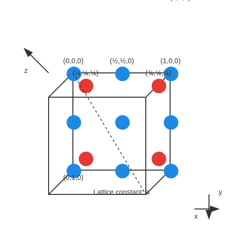
Silicon (Si) and germanium (Ge) are both Group IV elements with a diamond cubic crystal structure, where each atom forms four covalent bonds with its neighbors. The lattice constant of silicon is 5.431 Å, while germanium has a larger lattice constant of 5.658 Å due to its bigger atomic radius. The bandgap of these materials is a critical parameter in semiconductor physics:
At room temperature (300 K), silicon has an indirect bandgap of 1.12 eV, whereas germanium has a smaller indirect bandgap of 0.66 eV. This difference significantly impacts their applications—silicon's larger bandgap makes it more suitable for high-temperature and high-power devices, while germanium's narrower bandgap is advantageous for infrared detectors and low-voltage electronics.
Intrinsic Carrier Concentration
The intrinsic carrier concentration (ni) is exponentially dependent on temperature and bandgap:
Where NC and NV are the effective density of states in the conduction and valence bands, respectively. For silicon at 300 K, ni ≈ 1.5×1010 cm-3, while germanium has a much higher ni ≈ 2.4×1013 cm-3 due to its smaller bandgap. This higher intrinsic concentration makes germanium more susceptible to thermal noise in electronic devices.
Mobility and Resistivity
Charge carrier mobility (μ) is another key differentiator. Electrons in silicon have a mobility of ~1500 cm²/V·s, while holes move at ~450 cm²/V·s. Germanium exhibits higher mobilities—3900 cm²/V·s for electrons and 1900 cm²/V·s for holes—due to reduced effective mass and weaker lattice scattering. The resistivity (ρ) of intrinsic material is given by:
Where q is the electron charge, and n, p are electron and hole concentrations. High mobility makes germanium attractive for high-frequency applications, though silicon dominates due to its superior oxide interface properties.
Thermal and Chemical Stability
Silicon dioxide (SiO2) forms a stable, high-quality insulating layer when silicon is oxidized, a property absent in germanium. This native oxide was pivotal in silicon's dominance in MOSFET technology. Germanium oxides are water-soluble and unstable, requiring passivation techniques like germanium-on-insulator (GOI) for modern devices. Silicon also has a higher melting point (1414°C vs. 938°C for Ge), enabling robust high-temperature processing.
Applications and Modern Relevance
Silicon remains the cornerstone of integrated circuits, solar cells, and power devices. Germanium has seen a resurgence in:
- High-efficiency multijunction solar cells (combined with GaAs)
- Near-infrared optics and photodetectors
- Strained silicon-germanium (SiGe) heterojunction bipolar transistors (HBTs) for RF applications
Historical Context
Germanium was the first semiconductor used in transistors (1947 Bardeen-Brattain point-contact device), but silicon replaced it by the 1960s due to better thermal stability and oxide formation. Recent advances in epitaxial growth have revived germanium for niche applications where its superior mobility and optoelectronic properties outweigh processing challenges.
2.2 Compound Semiconductors (GaAs, InP, etc.)
Definition and Structural Properties
Compound semiconductors consist of two or more elements from different groups in the periodic table, typically combining elements from Group III (e.g., Ga, In) and Group V (e.g., As, P) or Group II (e.g., Cd, Zn) and Group VI (e.g., S, Se). Unlike elemental semiconductors like silicon (Si) or germanium (Ge), these materials exhibit a direct bandgap in many cases, enabling efficient light emission and absorption. The crystal structure is usually zincblende (cubic) or wurtzite (hexagonal), with tetrahedral coordination ensuring strong covalent-ionic bonding.
Bandgap Engineering and Electronic Properties
The bandgap \( E_g \) of compound semiconductors can be tuned by adjusting their composition. For ternary alloys like AlxGa1-xAs, the bandgap follows Vegard’s law:
where b is the bowing parameter accounting for nonlinear effects. GaAs, for instance, has a direct bandgap of 1.42 eV at 300 K, making it ideal for optoelectronic applications. In contrast, InP (1.34 eV) offers superior electron mobility and thermal stability for high-frequency devices.
Key Material Systems and Applications
- GaAs – Dominates RF and microwave electronics (e.g., HEMTs, MMICs) due to high electron mobility (≈8500 cm²/V·s). Also used in laser diodes and solar cells.
- InP – Critical for long-haul optical communication (1.55 µm wavelength) and terahertz devices. Its low effective mass enhances high-speed performance.
- GaN – Wide bandgap (3.4 eV) enables high-power, high-temperature applications (e.g., LEDs, power amplifiers).
- CdTe – Thin-film photovoltaics benefit from its near-ideal bandgap (1.5 eV) for solar energy conversion.
Heterostructures and Quantum Confinement
Epitaxial growth techniques (MBE, MOCVD) allow precise layering of compound semiconductors to form heterostructures. The discontinuity in band alignment at interfaces (Type-I, Type-II, or Type-III) enables quantum wells, dots, and superlattices. For a quantum well of thickness L, the quantized energy levels are:
where \( m^* \) is the effective mass. Such structures underpin modern optoelectronics, including quantum cascade lasers and high-electron-mobility transistors (HEMTs).
Challenges and Limitations
Despite their advantages, compound semiconductors face:
- High defect sensitivity – Dislocations degrade performance in lattice-mismatched systems (e.g., GaN on sapphire).
- Cost – Substrates (e.g., InP wafers) are expensive compared to silicon.
- Thermal management – Lower thermal conductivity than Si complicates power dissipation.
Emerging Trends
Research focuses on 2D materials (e.g., MoS2) integrated with III-V compounds, ultra-wide-bandgap materials (e.g., AlN), and molecular beam epitaxy (MBE) for atomic-scale precision. Applications span quantum computing (InAs/AlSb qubits) and neuromorphic devices.
2.3 Doping and Impurity Atoms
Intrinsic vs. Extrinsic Semiconductors
Intrinsic semiconductors, such as pure silicon or germanium, have limited conductivity due to their fixed number of charge carriers (electrons and holes) determined by thermal excitation. Extrinsic semiconductors, however, are engineered by deliberately introducing impurity atoms—a process called doping—to enhance conductivity by increasing the number of free charge carriers.
Donor and Acceptor Impurities
Doping involves two primary types of impurities:
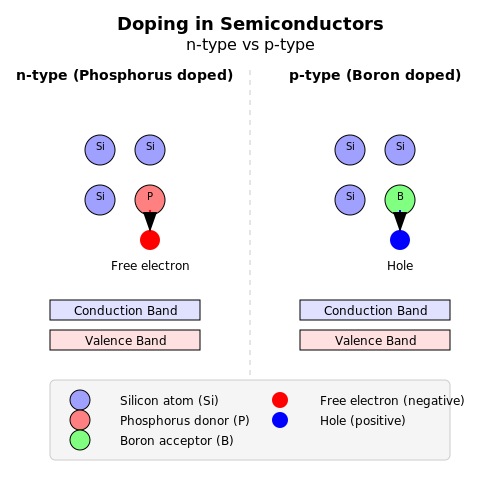
- Donor impurities (n-type doping): Atoms like phosphorus (P) or arsenic (As) from Group V of the periodic table donate extra electrons to the conduction band.
- Acceptor impurities (p-type doping): Atoms like boron (B) or gallium (Ga) from Group III accept electrons, creating holes in the valence band.
Carrier Concentration in Doped Semiconductors
The equilibrium electron (n) and hole (p) concentrations in a doped semiconductor are governed by mass-action law:
where ni is the intrinsic carrier concentration. For n-type doping, the majority carrier concentration is approximately equal to the donor concentration (Nd), while for p-type, it equals the acceptor concentration (Na).
Ionization Energy of Dopants
The energy required to ionize a donor or acceptor atom is significantly lower than the bandgap energy. For silicon, typical ionization energies are:
- Donors (e.g., P, As): ~0.045 eV
- Acceptors (e.g., B, Al): ~0.057 eV
This allows nearly complete ionization at room temperature, ensuring high carrier concentrations.
Doping Techniques and Practical Considerations
Common doping methods include:
- Diffusion: Impurity atoms are introduced at high temperatures and diffuse into the semiconductor lattice.
- Ion Implantation: Dopant ions are accelerated and embedded into the semiconductor, offering precise control over doping profiles.
Modern semiconductor fabrication relies heavily on ion implantation for its accuracy in defining transistor regions.
Compensation Doping
When both donor and acceptor impurities are present, the net doping concentration is:
This principle is exploited in device engineering to create regions with tailored conductivity, such as in p-n junctions or MOSFET channels.
3. Electrons and Holes
3.1 Electrons and Holes
Charge Carriers in Semiconductors
In semiconductors, charge transport is governed by two types of mobile carriers: electrons (negative charge) and holes (positive charge). An electron is a conduction band state occupied by an electron, while a hole is a valence band state vacated by an electron. The concept of holes arises from the quantum mechanical description of nearly-filled bands, where the absence of an electron behaves as a positively charged quasiparticle with effective mass mh.
Here, ni is the intrinsic carrier concentration, Nc and Nv are the effective density of states in the conduction and valence bands, Eg is the bandgap energy, k is Boltzmann's constant, and T is temperature. This equation shows the exponential dependence of carrier concentration on temperature and bandgap.
Generation and Recombination
Electron-hole pairs are generated when thermal or optical excitation promotes an electron from the valence band to the conduction band. The reverse process, recombination, occurs when an electron falls back into a hole, releasing energy as a photon (radiative) or phonons (non-radiative). The net recombination rate U is given by:
where τn and τp are carrier lifetimes, n1 and p1 are parameters dependent on trap energy levels, and n, p are the electron and hole concentrations.
Drift and Diffusion Currents
Carrier transport occurs via two mechanisms: drift (response to electric fields) and diffusion (response to concentration gradients). The total current density J is the sum of both components:
Here, μn, μp are mobilities, Dn, Dp are diffusion coefficients related by Einstein's relation D/μ = kT/q, and E is the electric field. In modern devices like MOSFETs, both mechanisms are critical—drift dominates in channel current, while diffusion governs subthreshold behavior.
Effective Mass and Band Structure
The curvature of energy bands determines carrier effective mass m* through the relation:
For silicon, the conduction band has six elliptical minima (Δ-valleys) leading to longitudinal (ml ≈ 0.98m0) and transverse (mt ≈ 0.19m0) effective masses. Holes exist in light and heavy bands (mlh ≈ 0.16m0, mhh ≈ 0.49m0), plus a split-off band. These values directly impact mobility and velocity saturation effects in nanoscale transistors.
3.2 Carrier Concentration and Mobility
Intrinsic Carrier Concentration
In an intrinsic semiconductor, the equilibrium electron (n) and hole (p) concentrations are equal and determined by the material's bandgap and temperature. The intrinsic carrier concentration ni is derived from the density of states in the conduction and valence bands and the Fermi-Dirac distribution:
where Nc and Nv are the effective density of states in the conduction and valence bands, respectively, Eg is the bandgap energy, k is Boltzmann's constant, and T is the temperature. For silicon at 300 K, ni ≈ 1.5 × 1010 cm−3.
Extrinsic Carrier Concentration
Doping introduces additional carriers, shifting the Fermi level. In an n-type semiconductor, donor impurities (e.g., phosphorus in silicon) increase the electron concentration:
where Nd is the donor concentration. Similarly, for p-type semiconductors with acceptor concentration Na, the hole concentration is:
The minority carrier concentration is determined by mass-action law:
Carrier Mobility
Carrier mobility (μ) quantifies how easily charge carriers move under an electric field. It is influenced by scattering mechanisms:
- Lattice scattering (phonon scattering): Dominates at high temperatures, with mobility ∝ T−3/2.
- Impurity scattering: Dominates at low temperatures or high doping, with mobility ∝ T3/2/Nd.
The net mobility is modeled by Matthiessen's rule:
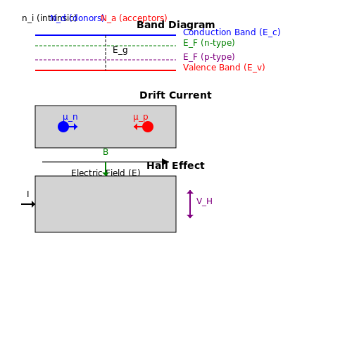
Drift Current and Conductivity
The drift current density J under an electric field E is:
where q is the electron charge, and μn, μp are electron and hole mobilities. The conductivity σ is:
In heavily doped silicon, mobility drops due to increased impurity scattering, peaking around 1017–1018 cm−3 before declining.
Hall Effect and Mobility Measurement
The Hall effect provides a direct method to measure carrier concentration and mobility. A perpendicular magnetic field B induces a Hall voltage VH:
where I is the current and t is the sample thickness. The Hall mobility is derived from:
3.3 Recombination and Generation Processes
Fundamental Mechanisms
In semiconductors, recombination and generation processes govern the dynamics of charge carriers (electrons and holes). These processes are critical in determining the minority carrier lifetime, photoconductivity, and the efficiency of optoelectronic devices. Recombination occurs when an electron in the conduction band transitions to the valence band, annihilating a hole. Conversely, generation involves the creation of an electron-hole pair, typically through thermal or optical excitation.
Types of Recombination
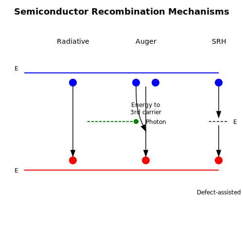
Three primary recombination mechanisms exist:
- Radiative Recombination: An electron recombines with a hole, emitting a photon. Governed by the direct bandgap transition probability, this mechanism dominates in materials like GaAs.
- Auger Recombination: The energy from electron-hole recombination is transferred to a third carrier (electron or hole), which thermalizes. This becomes significant at high carrier densities.
- Shockley-Read-Hall (SRH) Recombination: Occurs via defect states within the bandgap, acting as intermediate traps. The rate depends on the trap density and energy level.
Mathematical Formulation of SRH Recombination
The net recombination rate \( R \) for SRH processes is derived from trap-assisted transitions. For a single defect level at energy \( E_t \):
where:
- \( n \), \( p \): electron and hole concentrations
- \( n_i \): intrinsic carrier concentration
- \( au_n \), \( au_p \): carrier lifetimes
- \( n_1 = N_c e^{(E_t - E_c)/kT} \), \( p_1 = N_v e^{(E_v - E_t)/kT} \): parameters dependent on trap energy.
Generation Processes
Generation is the inverse of recombination and is thermally activated:
where \( E_g \) is the bandgap and \( \alpha \) is a material-specific constant. Optical generation follows the Beer-Lambert law, with a rate proportional to the incident photon flux and absorption coefficient.
Practical Implications
In solar cells, minimizing SRH recombination via defect passivation improves efficiency. In LEDs, maximizing radiative recombination enhances light output. Auger recombination limits the performance of high-power lasers and bipolar transistors at high currents.
Case Study: Silicon vs. Gallium Arsenide
Silicon’s indirect bandgap favors SRH recombination, making it unsuitable for efficient light emission. GaAs, with its direct bandgap, exhibits strong radiative recombination, ideal for lasers and LEDs. The minority carrier lifetime in Si is typically microseconds, while in GaAs, it is nanoseconds due to higher radiative efficiency.
4. Diodes and PN Junctions
4.1 Diodes and PN Junctions
Formation of the PN Junction
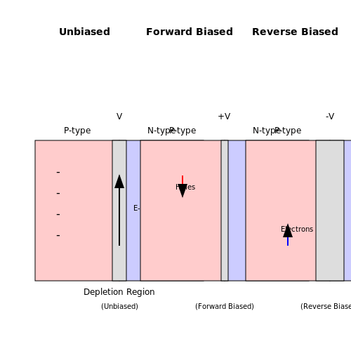
When a p-type semiconductor (doped with acceptors, creating excess holes) is brought into direct contact with an n-type semiconductor (doped with donors, creating excess electrons), a depletion region forms at the junction. The concentration gradient causes electrons to diffuse from the n-side to the p-side and holes to diffuse in the opposite direction. This leaves behind ionized dopants (fixed charges), creating an electric field that opposes further diffusion.
The built-in potential \( V_{bi} \) can be derived from the balance between diffusion and drift currents:
Current-Voltage Characteristics
Under forward bias (\( V > 0 \)), the potential barrier is reduced, allowing majority carriers to diffuse across the junction. The current follows the Shockley diode equation:
where \( I_0 \) is the reverse saturation current and \( n \) is the ideality factor (typically 1-2). Under reverse bias (\( V < 0 \)), the current saturates at \( -I_0 \) until breakdown occurs.
Breakdown Mechanisms
At high reverse voltages, two breakdown mechanisms dominate:
- Avalanche breakdown: Occurs when carriers gain sufficient energy to create electron-hole pairs via impact ionization. The critical field is given by:
- Zener breakdown: Dominates in heavily doped junctions where tunneling through the narrow depletion region occurs.
Small-Signal Model
For AC analysis, the diode is linearized around its operating point. The dynamic resistance \( r_d \) is:
The junction capacitance comprises:
- Depletion capacitance (\( C_j \)): Voltage-dependent capacitance from the space-charge region.
- Diffusion capacitance (\( C_d \)): From minority carrier storage under forward bias.
Practical Considerations
Real diodes exhibit non-ideal effects:
- Series resistance: Due to bulk semiconductor resistance.
- Recombination-generation currents: In the depletion region.
- Temperature dependence: \( I_0 \) doubles approximately every 10°C.
Applications
PN junctions form the basis for:
- Rectifiers in power supplies
- Clipping/clamping circuits
- Voltage references (Zener diodes)
- Photodiodes and solar cells
- Varactors for tuning circuits
4.2 Bipolar Junction Transistors (BJTs)
Structure and Operation
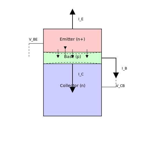
A Bipolar Junction Transistor (BJT) consists of three doped semiconductor regions: the Emitter, Base, and Collector, forming either an NPN or PNP configuration. The base-emitter junction is forward-biased, while the base-collector junction is reverse-biased in active mode operation. Minority carrier diffusion across the base region governs current amplification, quantified by the current gain parameters β (common-emitter) and α (common-base).
Current-Voltage Relationships
The Ebers-Moll model describes BJT operation through two coupled diode equations. For an NPN transistor in active mode:
where IS is the saturation current, VT the thermal voltage (~26 mV at 300K), and αF, βR the forward/reverse current gains.
Small-Signal Model
For AC analysis, the hybrid-π model represents the BJT with transconductance gm and output resistance ro:
where VA is the Early voltage. This model enables analysis of voltage/current gain, input/output impedance, and frequency response in amplifier circuits.
Switching Characteristics
In saturation mode (both junctions forward-biased), BJTs operate as low-resistance switches. Key metrics include:
- Turn-on delay (td(on)): Time to charge the base-emitter capacitance
- Rise time (tr): Collector current transition from 10% to 90%
- Storage time (ts): Minority carrier evacuation during turn-off
High-Frequency Behavior
The current gain cutoff frequency fT marks where |β| drops to unity, determined by charge transport delays:
where Cπ (base-emitter capacitance) and Cμ (base-collector capacitance) dominate high-frequency roll-off. Modern RF BJTs achieve fT > 300 GHz through heterojunction designs.
Thermal Considerations
Power dissipation PD = VCEIC raises junction temperature, impacting:
- Current gain (β increases ~1%/°C for Si)
- Leakage currents (doubles every ~10°C)
- Safe Operating Area (SOA) limits
Thermal runaway occurs when increased IC causes further heating—mitigated by emitter ballasting or temperature compensation.
Practical Applications
BJTs remain essential in:
- Analog circuits: Differential pairs, current mirrors, and power amplifiers
- Switching regulators: Darlington configurations for high-current drives
- RF systems: Low-noise amplifiers (LNAs) up to millimeter-wave bands
The Gummel-Poon model extends Ebers-Moll to account for high-level injection and base-width modulation, critical for precision SPICE simulations.
4.3 Field-Effect Transistors (FETs)
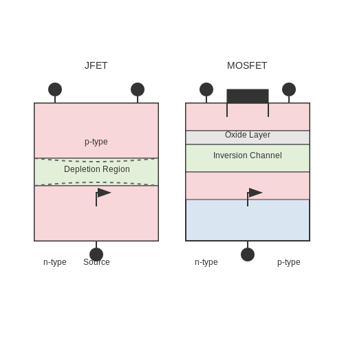
Field-effect transistors (FETs) are three-terminal semiconductor devices that regulate current flow via an electric field applied to a control terminal. Unlike bipolar junction transistors (BJTs), FETs operate with majority carriers only, resulting in high input impedance and lower power consumption. Two primary categories dominate modern applications: the junction field-effect transistor (JFET) and the metal-oxide-semiconductor FET (MOSFET).
JFET Operation Principles
JFETs consist of a doped semiconductor channel (n-type or p-type) with gate regions forming p-n junctions. Applying a reverse bias to the gate-channel junction modulates the depletion region width, controlling channel conductivity. The drain current \(I_D\) in the saturation region follows:
where \(I_{DSS}\) is the saturation current at \(V_{GS} = 0\), \(V_{GS}\) the gate-source voltage, and \(V_P\) the pinch-off voltage. Transconductance \(g_m\), a critical small-signal parameter, is derived as:
MOSFET Physics and Threshold Voltage
MOSFETs utilize an insulated gate electrode to induce a conductive channel via field effect. The threshold voltage \(V_{TH}\), defining the onset of strong inversion, depends on:
where \(\phi_{MS}\) is the metal-semiconductor work function difference, \(\phi_B\) the bulk potential, \(N_A\) the substrate doping, and \(C_{ox}\) the oxide capacitance per unit area. Modern nanoscale MOSFETs exhibit quantum mechanical effects that necessitate corrections to this classical model.
Short-Channel Effects
As MOSFET channel lengths shrink below 100 nm, phenomena like velocity saturation and drain-induced barrier lowering (DIBL) become significant. The saturation current \(I_{Dsat}\) under velocity saturation conditions follows:
where \(W\) is the channel width and \(v_{sat}\) the saturation velocity (~107 cm/s for silicon).
Advanced FET Architectures
Modern ICs employ non-planar FET designs to mitigate short-channel effects:
- FinFETs: Vertical fins provide enhanced gate control with 3D electrostatics
- Gate-all-around (GAA) FETs: Nanowire channels surrounded by gate material
- Tunnel FETs: Leverage band-to-band tunneling for sub-60 mV/decade switching
These devices enable continued scaling per Moore's Law while addressing power density challenges. The subthreshold swing \(S\), a key figure of merit, is given by:
where \(C_{dep}\) is the depletion capacitance. Novel materials like high-κ dielectrics (HfO2) and high-mobility channels (Ge, III-V compounds) further enhance performance.
5. Integrated Circuits (ICs)
5.1 Integrated Circuits (ICs)
Definition and Fabrication
An integrated circuit (IC) is a monolithic semiconductor device that incorporates multiple electronic components—such as transistors, resistors, capacitors, and diodes—into a single substrate, typically silicon. The fabrication process involves photolithography, doping, etching, and metallization to create interconnected layers of semiconductor material. The most common manufacturing technique is CMOS (Complementary Metal-Oxide-Semiconductor), which enables high-density, low-power digital and analog circuits.
Types of ICs
ICs are broadly classified into three categories:
- Analog ICs – Process continuous signals (e.g., operational amplifiers, voltage regulators).
- Digital ICs – Operate with discrete binary states (e.g., microprocessors, FPGAs).
- Mixed-Signal ICs – Combine analog and digital functions (e.g., ADCs, DACs).
Key Metrics and Performance Parameters
The performance of an IC is characterized by:
- Transistor Count – From a few (SSI) to billions (VLSI) of transistors.
- Power Dissipation – Governed by dynamic and static power consumption:
- Propagation Delay – Time taken for a signal to traverse a logic gate:
Moore’s Law and Scaling Trends
Moore’s Law predicts a doubling of transistor density every two years, driven by advancements in lithography (e.g., EUV). However, as feature sizes approach atomic limits (~3 nm node), quantum effects such as tunneling and leakage currents become significant, necessitating novel materials (e.g., FinFETs, GAAFETs) and architectures (e.g., 3D ICs).
Applications and Case Studies
ICs are foundational in modern electronics:
- Microprocessors – Multi-core CPUs with cache hierarchies.
- Memory ICs – DRAM, NAND flash, and emerging non-volatile technologies (ReRAM, MRAM).
- RF ICs – 5G transceivers leveraging SiGe and GaAs.
Design Methodologies
IC design follows a hierarchical flow:
- System-Level Design – Architectural simulation (e.g., MATLAB, SystemVerilog).
- RTL Synthesis – HDL-to-netlist conversion (e.g., Verilog, VHDL).
- Physical Design – Place-and-route (e.g., Cadence Innovus).
- Verification – Formal methods and tape-out validation.
Emerging Technologies
Beyond silicon, research focuses on:
- Quantum ICs – Superconducting qubits for quantum computing.
- Neuromorphic ICs – Spiking neural networks mimicking biological systems.
- Flexible Electronics – Organic and 2D materials (e.g., graphene, MoS₂).
5.2 Optoelectronic Devices (LEDs, Photodiodes)
Light-Emitting Diodes (LEDs)
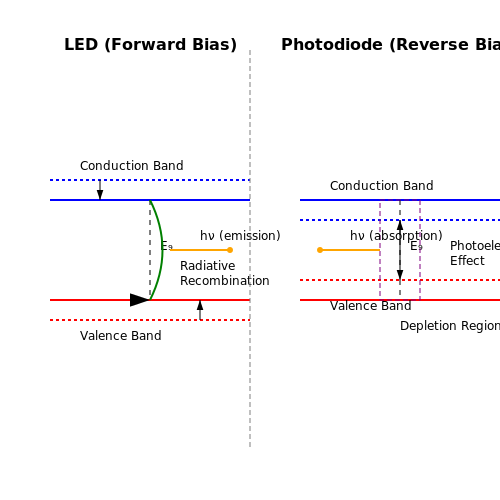
LEDs are semiconductor devices that emit incoherent narrow-spectrum light when forward-biased, operating on the principle of electroluminescence. The emitted photon energy Eph corresponds to the bandgap Eg of the semiconductor material:
where h is Planck's constant and ν is the photon frequency. For a p-n junction under forward bias, minority carrier injection leads to radiative recombination in the depletion region. The spectral emission wavelength λ is determined by:
with c being the speed of light. Modern high-efficiency LEDs employ direct bandgap materials like GaAs (infrared), GaP (red/green), and InGaN (blue/UV), often grown epitaxially with quantum well structures to enhance radiative recombination.
LED Efficiency Considerations
The internal quantum efficiency ηint is defined as the ratio of radiative recombination events to total carrier injections:
where Rr and Rnr are the radiative and non-radiative recombination rates respectively. The external quantum efficiency further accounts for photon extraction losses due to total internal reflection at semiconductor-air interfaces. Advanced packaging techniques like hemispherical lenses and photonic crystals are employed to improve light extraction.
Photodiodes: Principles of Operation
Photodiodes operate in reverse bias (photoconductive mode) or zero bias (photovoltaic mode), converting incident photons into electron-hole pairs through the photoelectric effect. The quantum efficiency η relates the number of collected charge carriers to incident photons:
where Iph is the photocurrent, Popt is the incident optical power, and q is the electron charge. The responsivity R (A/W) is given by:
with λ in nanometers. High-speed photodiodes utilize thin depletion regions and low-capacitance designs, while high-sensitivity devices employ avalanche multiplication (APDs) or heterostructures.
Noise Characteristics in Photodiodes
The total noise current in a photodiode includes shot noise from the dark current Id and photocurrent Iph, as well as thermal noise:
where Δf is the bandwidth, RL is the load resistance, and kT is the thermal energy. The noise-equivalent power (NEP) represents the minimum detectable power at unity signal-to-noise ratio:
Device Structures and Applications
Modern optoelectronic devices employ sophisticated heterostructures:
- Resonant-cavity LEDs use distributed Bragg reflectors to enhance directionality
- Vertical-cavity surface-emitting lasers (VCSELs) combine LED-like fabrication with laser coherence
- PIN photodiodes feature intrinsic layers for improved quantum efficiency
- Avalanche photodiodes (APDs) achieve internal gain through impact ionization
These devices find applications in optical communications (850-1550 nm bands), LiDAR systems (905-1550 nm), biomedical sensing, and solid-state lighting (visible spectrum). Emerging quantum dot LEDs and single-photon avalanche diodes (SPADs) are pushing the boundaries of efficiency and detection sensitivity.
5.3 Power Electronics and Solar Cells
Power Semiconductor Devices
Power electronics relies on semiconductor devices capable of handling high voltages and currents. The primary components include:
- Power Diodes - Optimized for high reverse breakdown voltages (up to several kV) and fast recovery times.
- Power MOSFETs - Used for high-frequency switching applications due to low gate drive power and fast switching speeds.
- IGBTs - Combine the high input impedance of MOSFETs with the low conduction losses of BJTs, ideal for medium to high power applications.
- Thyristors - Including SCRs and TRIACs, used in AC power control applications.
The figure-of-merit for power devices is the Baliga's Figure of Merit (BFOM):
where \(E_{br}\) is the breakdown electric field, \(\mu_n\) is the electron mobility, and \(\epsilon_s\) is the semiconductor permittivity.
Solar Cell Physics
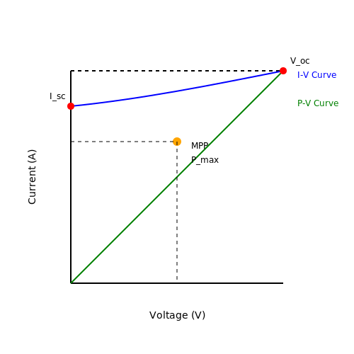
Photovoltaic cells operate based on the photovoltaic effect where electron-hole pairs are generated by photon absorption. The key parameters are:
- Short-circuit current (Isc) - Maximum current under zero voltage bias
- Open-circuit voltage (Voc) - Maximum voltage under zero current
- Fill factor (FF) - Ratio of maximum power to (Isc × Voc)
The ideal solar cell current-voltage relationship is given by:
where \(I_L\) is the light-generated current, \(I_0\) is the reverse saturation current, \(n\) is the ideality factor, and \(kT/q\) is the thermal voltage.
Maximum Power Point Tracking
To extract maximum power from solar cells under varying illumination conditions, MPPT algorithms are employed. The most common techniques include:
- Perturb and Observe - Periodically adjusts voltage and measures power changes
- Incremental Conductance - Compares instantaneous conductance to incremental conductance
- Fractional Open-Circuit Voltage - Uses empirical relationship between Voc and Vmp
The power converter duty cycle (\(D\)) for maximum power transfer is derived from:
where \(V_{in}\) is the solar panel voltage and \(V_{out}\) is the load voltage.
Wide Bandgap Semiconductors
Modern power electronics increasingly uses wide bandgap materials:
| Material | Bandgap (eV) | Breakdown Field (MV/cm) |
|---|---|---|
| SiC | 3.26 | 2.5 |
| GaN | 3.44 | 3.3 |
| Diamond | 5.47 | 10 |
The Baliga's figure of merit comparison shows SiC is 10× and GaN is 1000× better than silicon for power devices.
Thermal Management
Power dissipation in semiconductor devices follows:
where \(R_{on}\) is the on-resistance, \(V_{off}\) is the blocking voltage, and \(f_{sw}\) is the switching frequency. Effective heat sinking is critical, with thermal resistance given by:
6. Recommended Textbooks
6.1 Recommended Textbooks
- PDF Introduction to Semiconductor Devices - Cambridge University Press ... — 6 Metal-insulator-semiconductor structures and MOSFETs 127 6.1 MIS systems in equilibrium 127 6.2 MIS systems under bias 133 6.3 Basic theory of MOSFET operation 144 6.4 Small signal operation of MESFETs and MOSFETs 155 6.5 CMOS circuits 160 Problems 165 7 Short-channel effects and challenges to CMOS 169 7.1 Short-channel effects 169
- PDF Semiconductor Basics - content.e-bookshelf.de — 1.4 The Classifications of Basic Elements 5 1.5 The Hydrogen Spectrum Lines 5 1.6 Light is a Particle 7 1.7 The Atom's Structure 8 1.8 The Bohr Atom 10 1.9 Summary and Conclusions 13 Appendix 1.1 Some Details of the Bohr Model 14 Appendix 1.2 Semiconductor Materials 16 Appendix 1.3 Calculating the Rydberg Constant 16 2 Energy Bands 19
- PDF Basics of Electronics - Tpu — BASICS OF ELECTRONICS It is recommended for publishing as a study aid ... Tomsk Polytechnic University Publishing House 2017 . 2 UDC 621.38(075.8) BBC 31.2 K58 Kozhemyak O.A. K58 Basics of electronics: study aid / O.A. Kozhemyak, D.N. ... 1 D.C. Circuits 6 1.1 Introduction 6 1.2 Electric Current, Electromotive Force, Potential Difference ...
- PDF Fundamentals of Semiconductor Devices - etextbook.to — 6.4 Metal-Semiconductor Junctions 323 6.4.1 Ideal Metal-Semiconductor Junctions (Electron Affinity Model) 323 6.4.2 Influence of Interface-Induced Dipoles 325 6.4.3 The Current-Voltage Characteristics of Metal-Semiconductor Junctions 326 6.4.4 Ohmic (Low-Resistance) Contacts 330 6.4.5 I-V a Characteristics of Heterojunction Diodes 331
- Semiconductor Basics[Book] - O'Reilly Media — An accessible guide to how semiconductor electronics work and how they are manufactured, for professionals and interested readers with no electronics engineering background. Semiconductor Basics is an accessible guide to how semiconductors work. It is written for readers without an electronic engineering background.
- Solid State Electronic Devices, 7th edition - Pearson — One of the most widely used introductory books on semiconductor materials, physics, devices and technology, Solid State Electronic Devices aims to: 1) develop basic semiconductor physics concepts, so students can better understand current and future devices; and 2) provide a sound understanding of current semiconductor devices and technology ...
- PDF Fundamentals of Semiconductors: Physics and Materials Properties, 4th ... — Physics for the year 2000 has been awarded to two semiconductor physicists, Zhores I. Alferov and Herbert Kroemer ("for developing semiconductor het-erostructures used in high-speed- and opto-electronics") and a semiconductor device engineer, Jack S. Kilby ("for his part in the invention of the integrated circuit").
- PDF Basic Electronics for Scientists and Engineers — Basic Electronics for Scientists and Engineers Ideal for a one-semester course, this concise textbook covers basic electronics for undergraduate students in science and engineering. Beginning with basics of general circuit laws and resistor circuits to ease students into the subject, the textbook then covers a wide range of topics,
- Semiconductor Devices: Theory and Application - Open Textbook Library — The goal of this text, as its name implies, is to allow the reader to become proficient in the analysis and design of circuits utilizing discrete semiconductor devices. It progresses from basic diodes through bipolar and field effect transistors. The text is intended for use in a first or second year course on semiconductors at the Associate or Baccalaureate level. In order to make effective ...
- Understanding Semiconductors: A Technical Guide for Non-Technical ... — Overall, this book is an excellent resource for people working in the semiconductor, electronics, and hardware technologies fields or in supporting industries. Additionally, it is an excellent guide for hobbyists and enthusiasts with minimal technical experience or pre-existing qualifications like myself, and anyone interested in learning more ...
6.2 Research Papers and Journals
- PDF Fundamentals of Semiconductor Devices - etextbook.to — 6.4 Metal-Semiconductor Junctions 323 6.4.1 Ideal Metal-Semiconductor Junctions (Electron Affinity Model) 323 6.4.2 Influence of Interface-Induced Dipoles 325 6.4.3 The Current-Voltage Characteristics of Metal-Semiconductor Junctions 326 6.4.4 Ohmic (Low-Resistance) Contacts 330 6.4.5 I-V a Characteristics of Heterojunction Diodes 331
- Basics of Semiconductor Process Tech - Academia.edu — Basics of Semiconductor Process Technology Version 2.0 by Harlan McGhan This document is intended to provide a basic background in the nature, operation, and manufacture of semiconductor devices, including the rules that govern the scaling of such devices and long-term industry trends. ... 6 2.1 Nature of a Transistor ..... 6 2.2 Types of ...
- Chip Design 2020 | IEEE Journals & Magazine | IEEE Xplore — Electronic ISSN: 1937-4143 INSPEC Accession Number: ... This special issue of IEEE Micro aimed at publishing some of the most significant research that can highlight the trends in IC design in 2020 and provide direct ... Journals & Magazines > IEEE Micro > Volume: 40 Issue: 6. Chip Design 2020. Publisher: IEEE. Cite This. PDF.
- (PDF) Semiconductor - Academia.edu — Academia.edu is a platform for academics to share research papers. Semiconductor ... The semiconductor electronics field continues to be a fast-changing one, with thousands of technical papers published each year. ... J. Semiconductor Ursices: Basic Princip1e.r New York: John Wiley and Sons, 2001. Streetman, B. G., and S. Banerjee. Solid State ...
- (PDF) SEMICONDUCTOR DEVICE FUNDAMENTALS - Academia.edu — check Save papers to use in your research. ... Sydney • Singapore • Tokyo • Madrid • San Juan • Milan • Paris CONTENTS General Introduction Part I Semiconductor Fundamentals Chapter 1 Semiconductors: A General Introduction 1.1 General Material Properties 1.1.1 Composition 1.1.2 Purity 1.1.3 Structure 1.2 Crystal Structure 1.2.1 The ...
- Electronic Surface Properties of Semiconductor Surfaces and ... - Springer — The lower V bi s (compared to V bi b) is most probably due to two main reasons: band bending due to semiconductor surface states, and/or external charge on the sample surface.Surface states (due to imperfect cleavage and/or oxides on the air exposed sample) can trap holes (electrons) on the cleaved surfaces of the p (n) sides of the junction, creating depletion type band bending opposite in ...
- PDF Fundamentals of Semiconductors: Physics and Materials Properties, 4th ... — 2) Reviews of the book in various magazines and journals. 3) Errata to both first and second printing (most have been corrected in the second edition as of this date). 4) Solutions to selected problems. 5) Additional supplementary problems. The solutions in item (4) are usually incomplete. They are supposed to serve as helpful hints and guides ...
- Semiconductor Devices: Theory and Application - Open Textbook Library — The goal of this text, as its name implies, is to allow the reader to become proficient in the analysis and design of circuits utilizing discrete semiconductor devices. It progresses from basic diodes through bipolar and field effect transistors. The text is intended for use in a first or second year course on semiconductors at the Associate or Baccalaureate level. In order to make effective ...
- PDF Semiconductor Basics - content.e-bookshelf.de — vii Acknowledgements xiii Introduction xv 1 The Bohr Atom 1 Objectives of This Chapter 1 1.1 Sinusoidal Waves 1 1.2 The Case of the Missing Lines 3 1.3 The Strange Behavior of Spectra from Gases and Metals 4 1.4 The Classifications of Basic Elements 5 1.5 The Hydrogen Spectrum Lines 5 1.6 Light is a Particle 7 1.7 The Atom's Structure 8 1.8 The Bohr Atom 10
- PDF Basics of Semiconductor Devices - IIT Bombay — dopants is called intrinsic. An unperturbed semiconductor must be charge neutral as a whole. If we denote the concentration of ionised donors by N+ d and the concentra-tion of ionised acceptors by N a, we can write for the net charge density at any point in the semiconductor as: ˆ = q(N+ d Na +p n) (1) where q is the absolute value of the ...
6.3 Online Resources and Tutorials
- PDF Semiconductor Basics - content.e-bookshelf.de — 1.4 The Classifications of Basic Elements 5 1.5 The Hydrogen Spectrum Lines 5 1.6 Light is a Particle 7 1.7 The Atom's Structure 8 1.8 The Bohr Atom 10 1.9 Summary and Conclusions 13 Appendix 1.1 Some Details of the Bohr Model 14 Appendix 1.2 Semiconductor Materials 16 Appendix 1.3 Calculating the Rydberg Constant 16 2 Energy Bands 19
- PDF Basic Electronics Tutorials - sttal.ac.id — Basic Electronics Tutorials ©2013 Basic Electronics Tutorials | www.electronics-tutorials.ws Page 4 1.3 ELECTRIC CURRENT Electric current is the flow of electric charge in the form of free electrons. Current is measured by the number of free electrons passing a particular point within a circuit per second.
- Introduction to Electronics - Coursera — Problem 6-3-1 • 30 minutes; Problem ... it's so much more than that. Coursera allows me to learn without limits." Learner reviews. 4.7. 2,521 reviews. 5 stars. 76.79%. 4 stars. 18.28%. 3 stars ... This is a beautiful course. Be the end of the course you would definitely get confidence with the basics of electronics and once complicated ...
- PDF Fundamentals of Semiconductors: Physics and Materials Properties, 4th ... — Physics for the year 2000 has been awarded to two semiconductor physicists, Zhores I. Alferov and Herbert Kroemer ("for developing semiconductor het-erostructures used in high-speed- and opto-electronics") and a semiconductor device engineer, Jack S. Kilby ("for his part in the invention of the integrated circuit").
- PDF Semiconductor Diode - talkingelectronics.com — Semiconductor Diode 77 6.1 Semiconductor Diode A pn junction is known as a semi-conductor or *crystal diode. The outstanding property of a crystal diode to conduct current in one direction only permits it to be used as a rectifier. A crystal diode is usually represented by the schematic symbol shown in Fig. 6.1. The arrow in the
- Semiconductor Devices: Theory and Application - Open Textbook Library — The goal of this text, as its name implies, is to allow the reader to become proficient in the analysis and design of circuits utilizing discrete semiconductor devices. It progresses from basic diodes through bipolar and field effect transistors. The text is intended for use in a first or second year course on semiconductors at the Associate or Baccalaureate level. In order to make effective ...
- Readings | Introductory Analog Electronics Laboratory | Electrical ... — Cathey, Jimmie J. Schaum's Outlines Electronic Devices and Circuits. 2nd ed. New York, NY: McGraw-Hill, 2002. ISBN: 9780071362702. Further reading on a wide variety of analog electronics topics is suggested in this list of references, compiled by the course staff. Readings by Session
- Lab 3 - Diodes | Instrumentation LAB — This is the first of three labs on basic semiconductor components. You will study semiconductor characteristics and some of their applications, leading up to the design and construction of a differential amplifier. Note: Keep all your parts with you, as they are for you permanently. DO NOT RETURN THEM TO THE CABINETS. This lab studies diodes.
- Basic Electronics - Quick Guide - Online Tutorials Library — Basic Electronics - Materials. Matter is made up of molecules which consists of atoms. According to Bohrs theory, the atom consists of positively charged nucleus and a number of negatively charged electrons which revolve round the nucleus in various orbits. When an electron is raised from a lower state to a higher state, it is said to be ...
- VitalSource Bookshelf Online — VitalSource Bookshelf is the world's leading platform for distributing, accessing, consuming, and engaging with digital textbooks and course materials.