Low Power Design
1. Power Consumption Metrics and Definitions
1.1 Power Consumption Metrics and Definitions
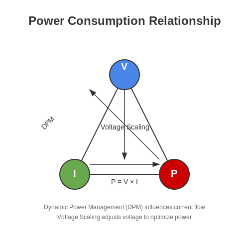
Power dissipation in electronic systems is governed by fundamental physical relationships and operational constraints. The instantaneous power P(t) consumed by a device is given by the product of voltage and current at any time t:
For DC systems, this simplifies to P = VI, while in AC circuits, the RMS values must be considered along with the power factor cos(θ):
Static vs. Dynamic Power
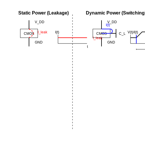
CMOS devices exhibit two primary power consumption mechanisms:
- Static power (Pstatic): Leakage current (Ileak) flowing when transistors are nominally off, given by:
$$ P_{static} = V_{DD} \cdot I_{leak} $$
- Dynamic power (Pdynamic): Switching energy dissipated during logic transitions, dominated by:
$$ P_{dynamic} = α C_L V_{DD}^2 f $$where α is activity factor, CL is load capacitance, and f is clock frequency.
Key Metrics for Low-Power Design
Several figures of merit quantify power efficiency:
| Metric | Definition | Units |
|---|---|---|
| Power-Delay Product (PDP) | $$ PDP = P_{avg} \cdot t_d $$ | J |
| Energy per Operation | $$ E_{op} = \frac{P_{avg}}{f_{op}} $$ | J/op |
| Energy-Delay Product (EDP) | $$ EDP = PDP \cdot t_d $$ | J·s |
Advanced Considerations
In nanometer-scale CMOS, short-channel effects introduce additional components:
Where short-circuit power occurs during finite transistor switching times, and glitching power arises from spurious transitions in combinatorial logic. Subthreshold leakage current follows:
with VT = kT/q being the thermal voltage (~26mV at 300K).
Practical Measurement Techniques
Accurate power characterization requires:
- Precision current sensing (shunt resistors/current mirrors)
- Time-domain integration for energy measurements
- Statistical methods for activity factor estimation
- Thermal imaging for spatial power distribution
1.2 Sources of Power Dissipation in Electronic Systems
Power dissipation in electronic systems arises from multiple physical mechanisms, each contributing to energy loss and heat generation. Understanding these sources is critical for optimizing low-power designs.
Dynamic Power Dissipation
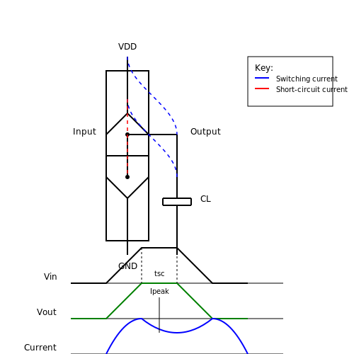
The dominant source of power consumption in digital CMOS circuits is dynamic power dissipation, which occurs during transistor switching. It consists of two components:
The switching component is given by:
where α is the activity factor, CL is the load capacitance, VDD is the supply voltage, and f is the clock frequency. The quadratic dependence on voltage makes voltage scaling particularly effective for power reduction.
The short-circuit component occurs when both NMOS and PMOS transistors are momentarily on during switching:
where Ipeak is the peak short-circuit current and tsc is the duration of the short-circuit condition.
Static Power Dissipation
As transistor sizes shrink, static power becomes increasingly significant. It includes:
- Subthreshold leakage: Current flowing between source and drain when the transistor is nominally off
- Gate leakage: Tunneling current through thin gate oxides
- Junction leakage: Reverse-biased diode leakage at drain/source junctions
The subthreshold leakage current follows:
where VT is the thermal voltage and n is the subthreshold slope factor.
Interconnect Power
Modern systems face increasing power losses in interconnects due to:
- Capacitive coupling between wires
- Resistive losses in narrow metal traces
- Inductive effects at high frequencies
The power dissipated in an interconnect can be modeled as:
Clock Distribution Power
Clock networks often consume 30-50% of total chip power due to:
- High switching activity (α ≈ 1)
- Large capacitive loads from global distribution
- Clock gating inefficiencies
The power in a clock tree with N buffers is:
I/O Power
Off-chip communication consumes significant power due to:
- Large voltage swings (often 1.8V-3.3V)
- High pad capacitance (1-10pF)
- Termination resistors for impedance matching
The power for driving a capacitive load CL through a transmission line is:
Analog Circuit Power
Analog components contribute power through:
- Bias currents in amplifiers
- Switching losses in data converters
- Filter resistor networks
For example, a class-A amplifier's power is:
where Psignal is the power delivered to the load.
1.3 Trade-offs Between Power, Performance, and Area (PPA)
In integrated circuit (IC) design, optimizing for power, performance, and area (PPA) requires careful balancing of competing constraints. These three factors are deeply interdependent, and improving one often degrades another. Understanding these trade-offs is critical for designing energy-efficient systems without sacrificing functionality or manufacturability.
Power-Performance Trade-offs
The relationship between power consumption and performance is governed by fundamental physics. Dynamic power in CMOS circuits is given by:
where α is the activity factor, CL is the load capacitance, VDD is the supply voltage, and f is the operating frequency. Reducing VDD quadratically lowers power but also decreases transistor drive current, which can be approximated as:
where Vth is the threshold voltage and γ is a velocity saturation factor (typically 1.3–2). This reduction in current forces a trade-off: lowering VDD saves power but reduces maximum operating frequency (fmax), degrading performance.
Area Considerations
Area optimization affects both power and performance. Smaller transistors reduce leakage power but increase current density, leading to higher dynamic power density. Conversely, larger transistors can improve performance by reducing resistance but increase parasitic capacitance. The optimal transistor sizing for minimum energy per operation often occurs at a point where:
where W is the transistor width and Etotal is the sum of dynamic and leakage energy.
Practical Design Strategies
Modern low-power designs employ several techniques to navigate PPA trade-offs:
- Voltage scaling: Adaptive voltage scaling adjusts VDD dynamically based on workload requirements.
- Multi-Vth designs: Using high-Vth transistors for leakage-critical paths and low-Vth devices for speed-critical paths.
- Power gating: Shutting off unused blocks reduces leakage but requires additional area for isolation cells.
- Architectural pipelining: Increasing pipeline stages allows lower voltage operation at the cost of area and control complexity.
Case Study: Mobile Processor PPA Optimization
A recent ARM Cortex-M7 implementation achieved a 40% power reduction through:
- Clock gating 85% of unused logic
- Implementing a dual-voltage domain (0.9V for logic, 1.1V for memory)
- Using high-density standard cells for non-critical paths
This came with a 15% area increase and 10% performance penalty in worst-case conditions, demonstrating the inherent compromises in PPA optimization.
Quantifying Trade-offs
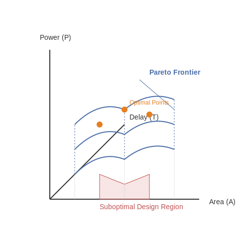
The Pareto frontier represents optimal PPA trade-offs, where improving one metric requires sacrificing another. For an N-design space, this can be expressed as:
where wi are weighting factors, and P, T, and A represent power, delay (1/performance), and area functions of design parameters x.
2. Voltage Scaling and Multi-VDD Design
2.1 Voltage Scaling and Multi-VDD Design
Fundamentals of Voltage Scaling
The dynamic power dissipation in a CMOS circuit is given by:
where α is the activity factor, CL is the load capacitance, VDD is the supply voltage, and f is the operating frequency. Since power scales quadratically with voltage, reducing VDD is the most effective way to lower power consumption. However, this comes at the cost of increased delay:
where Vth is the threshold voltage and α is the velocity saturation index (typically 1.3–2).
Multi-VDD Design Strategies
Multi-VDD design partitions a system into voltage domains, each operating at its minimum feasible voltage. Critical paths use higher VDD to meet timing constraints, while non-critical paths operate at lower voltages. Key implementation methods include:
- Static Voltage Scaling (SVS): Fixed voltage domains determined at design time
- Dynamic Voltage Scaling (DVS): Real-time voltage adjustment based on workload
- Adaptive Voltage Scaling (AVS): Closed-loop control using performance monitors
Voltage Island Implementation
Creating voltage islands requires:
- Level shifters at domain crossings
- Power switches for island isolation
- Separate power routing and grid design
The optimal number of voltage domains balances power savings against area overhead from level shifters and power management circuitry.
Practical Considerations
In 28nm CMOS implementations, Multi-VDD designs achieve 25–40% power reduction compared to single-VDD designs. Key challenges include:
- IR drop variation across voltage domains
- Timing closure complexity
- Increased design verification effort
Advanced Techniques
Recent research combines voltage scaling with:
- Near-threshold computing for ultra-low-power domains
- Machine learning predictors for DVS decision making
- 3D IC implementations with tier-specific voltage optimization
where η represents the theoretical maximum power saving efficiency when scaling from Vhigh to Vlow.
2.2 Clock Gating and Power Gating
Clock Gating: Dynamic Power Reduction
Clock gating is a technique used to disable the clock signal to idle circuit blocks, reducing dynamic power consumption. Since dynamic power in CMOS circuits is given by:
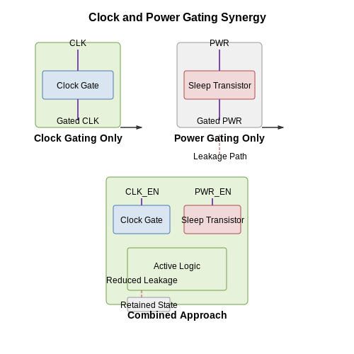
where α is the activity factor, C is the load capacitance, V is the supply voltage, and f is the clock frequency. By gating the clock (f = 0), dynamic power drops to zero for inactive modules. Modern synthesis tools automatically insert clock gating cells (e.g., AND/OR-based enable logic) when detecting registers with common enable conditions.
Power Gating: Leakage Suppression
Power gating physically disconnects unused blocks from the power supply using high-Vth header/footer switches. Leakage current in deep-submicron nodes follows:
Power gating reduces VDS to near-zero for gated blocks, exponentially cutting leakage. Two implementations dominate:
- Fine-grained: Individual sleep transistors per standard cell (higher area overhead)
- Coarse-grained: Shared sleep transistors for entire macros (longer wakeup latency)
State Retention and Wakeup Overhead
Power-gated designs often use retention flip-flops to preserve critical state during sleep mode. Wakeup energy (Ewake) must be amortized over sleep duration (Tsleep) for net savings:
Industrial implementations like Intel's VTCMOS and TSMC's MTCMOS achieve 10-100× leakage reduction with < 5% performance penalty.
Synergistic Application
Combining both techniques optimizes total power:
For example, ARM's Big.Little architecture gates clocks to inactive CPU cores while power-gating entirely idle clusters.
2.3 Subthreshold and Near-Threshold Operation
Subthreshold and near-threshold operation exploit the weak inversion region of MOSFETs to achieve ultra-low power consumption, trading off performance for energy efficiency. These techniques are critical in applications like biomedical implants, IoT sensors, and energy-harvesting systems where power budgets are stringent.
Subthreshold Operation
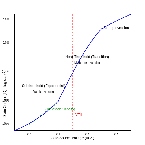
In subthreshold operation, the transistor operates below its threshold voltage (VTH), where the drain current (ID) is dominated by diffusion rather than drift. The current-voltage relationship follows an exponential law:
Here, I0 is a process-dependent parameter, n is the subthreshold slope factor (typically 1.2–1.6), and ϕT is the thermal voltage (~26 mV at 300 K). The subthreshold slope (S) defines the voltage swing needed to change the current by one decade:
Key challenges include increased sensitivity to process variations, temperature fluctuations, and reduced drive current. However, the quadratic reduction in dynamic power (Pdyn ∝ VDD2) makes subthreshold operation attractive for duty-cycled systems.
Near-Threshold Operation
Near-threshold operation balances energy efficiency and performance by biasing the transistor close to VTH. The drain current exhibits a mix of weak and strong inversion characteristics:
This region offers a 5–10× improvement in energy per operation compared to super-threshold designs while maintaining usable speed. However, delay variability increases due to the steep ID-VGS slope, requiring careful statistical design.
Practical Considerations
- Leakage-Delay Tradeoff: Subthreshold circuits minimize active power but suffer from higher leakage and slower switching. Near-threshold designs strike a compromise.
- Variability Mitigation: Techniques like body biasing, adaptive voltage scaling, and error-tolerant logic are essential to manage threshold voltage variations.
- Circuit Topologies:
- Subthreshold: Ring oscillators, level shifters, and ultra-low-power SRAM.
- Near-threshold: Parallelized architectures, voltage stacking, and resilient pipelines.
Applications
Subthreshold and near-threshold techniques are used in:
- Wireless sensor nodes (e.g., Zigbee, LoRa).
- Biomedical devices (e.g., pacemakers, neural recorders).
- Energy-harvesting systems (e.g., solar/RF-powered microcontrollers).
3. Dynamic Voltage and Frequency Scaling (DVFS)
3.1 Dynamic Voltage and Frequency Scaling (DVFS)
Dynamic Voltage and Frequency Scaling (DVFS) is a power management technique that adjusts a processor's operating voltage and frequency in real-time based on workload demands. The underlying principle stems from the relationship between dynamic power consumption, voltage, and frequency:
where Pdynamic is the dynamic power, α is the activity factor, C is the load capacitance, V is the supply voltage, and f is the operating frequency. Since power scales quadratically with voltage and linearly with frequency, reducing either parameter significantly lowers energy consumption.
Voltage-Frequency Coupling
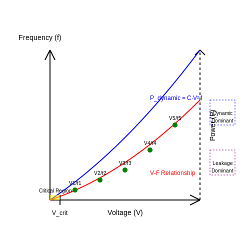
In CMOS circuits, the maximum operating frequency (fmax) is constrained by the supply voltage due to transistor switching characteristics. The delay of a CMOS gate is approximated by:
where Vth is the threshold voltage, and β and α are technology-dependent parameters. For stable operation, frequency must be scaled proportionally with voltage to avoid timing violations.
Implementation Strategies
DVFS is implemented through closed-loop control systems that monitor processor utilization and adjust voltage-frequency pairs (V-f points) dynamically. Modern systems use predefined V-f tables validated during silicon characterization. Key implementation approaches include:
- Discrete DVFS: Switches between predefined V-f operating points (e.g., ARM big.LITTLE).
- Continuous DVFS: Adjusts voltage and frequency in fine-grained steps (e.g., Intel SpeedShift).
- Per-Core DVFS: Independent scaling for individual cores in multi-core processors.
Energy-Quality Tradeoffs
DVFS introduces a tradeoff between energy efficiency and computational throughput. The energy per operation (Eop) is minimized at the critical voltage (Vcrit), derived by solving:
Below Vcrit, leakage energy dominates; above it, dynamic energy becomes prohibitive.
Real-World Case Studies
Commercial implementations demonstrate DVFS effectiveness:
- Mobile Processors: Qualcomm Snapdragon uses 100+ V-f points for 30-50% power savings.
- Data Centers: Google's Borg system employs DVFS to reduce cluster-wide energy by 15%.
- Embedded Systems: TI's MSP430 achieves sub-mW operation via ultra-fine voltage scaling.
Challenges and Limitations
While DVFS provides substantial energy savings, practical challenges include:
- Voltage regulator response time (10-100 µs latency).
- Stability constraints during V-f transitions.
- Nonlinearities in deep submicron technologies (e.g., 5nm FinFET).
3.2 Power-Aware Scheduling and Task Migration
Power-aware scheduling optimizes energy consumption by dynamically assigning computational tasks to processing elements based on workload, thermal constraints, and power budgets. Task migration extends this by redistributing active workloads across cores or clusters to balance performance and efficiency.
Dynamic Voltage and Frequency Scaling (DVFS) in Scheduling
DVFS reduces power consumption by scaling voltage and frequency according to workload demands. The power dissipated in a CMOS processor is given by:
where C is the switched capacitance, V is the supply voltage, f is the operating frequency, and Ileak is the leakage current. A scheduler exploiting DVFS must solve:
where Ei(t) is the energy consumed by task i at time t, and Ti is its execution time.
Task Migration for Thermal and Power Balancing
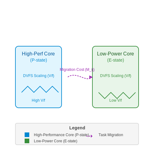
Heterogeneous multicore systems leverage task migration to shift workloads from power-hungry cores to more efficient ones. The migration cost M between cores i and j depends on:
where α and β are architecture-dependent coefficients. Optimal migration minimizes:
with γ weighting the migration penalty against power savings.
Real-World Implementations
Linux’s Energy-Aware Scheduler (EAS) integrates DVFS and task placement using per-entity load tracking (PELT). ARM’s big.LITTLE architecture migrates tasks between high-performance and low-power cores, achieving up to 40% energy reduction for mobile workloads.
Challenges and Trade-offs
- Latency vs. Energy: Frequent migrations increase overhead but improve load balancing.
- Predictive Accuracy: Machine learning models predict task durations to guide scheduling, but mispredictions degrade efficiency.
- Hardware Support: Cache coherence and inter-core interrupts add complexity to migration.
Memory Hierarchy Optimization for Low Power
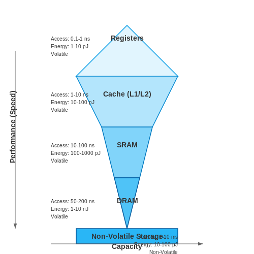
Memory hierarchy optimization is a critical aspect of low-power design, particularly in advanced computing systems where memory access dominates energy consumption. The goal is to minimize power dissipation while maintaining performance by strategically organizing memory subsystems—registers, caches, SRAM, DRAM, and non-volatile storage—based on access frequency and energy cost.
Energy-Aware Memory Access Patterns
The energy consumed during memory access is modeled by:
where Nread and Nwrite are the number of read/write operations, Eread and Ewrite are the respective energy costs per operation, and Eleakage is the static power dissipation during idle periods. Optimizing this equation involves:
- Reducing access frequency through data locality enhancement.
- Minimizing writes by employing write-back caches or non-volatile memory.
- Lowering leakage via power gating or dynamic voltage scaling.
Cache Optimization Techniques
Caches account for a significant portion of processor power. Key strategies include:
- Way-prediction: Reducing energy by predicting which cache way will be accessed.
- Sub-banking: Partitioning cache into smaller banks, activating only the necessary sections.
- Selective cache disabling: Turning off unused cache lines dynamically.
The energy savings from sub-banking can be quantified as:
where k is the number of sub-banks and Ebank_select is the overhead of bank selection logic.
DRAM Power Reduction
DRAM power is dominated by refresh cycles and row activation energy. Techniques include:
- Partial array self-refresh (PASR): Refreshing only active memory segments.
- Bank parallelism: Distributing accesses to minimize row activations.
- Low-power modes: Transitioning to standby or power-down states during idle periods.
The refresh power for PASR is given by:
where α is the fraction of refreshed arrays, Ctotal is the total capacitance, and frefresh is the refresh frequency.
Non-Volatile Memory Integration
Emerging non-volatile memories (e.g., STT-MRAM, ReRAM) offer near-zero leakage and high density. Challenges include:
- Write endurance: Limited write cycles in resistive memories.
- Asymmetric read/write energy: High write energy compared to reads.
Hybrid memory systems combine volatile and non-volatile memory, optimizing placement based on access patterns. The energy trade-off is:
where fi is the access frequency for non-volatile blocks.
Real-World Applications
Modern processors like ARM Cortex-M series employ hierarchical memory shutdown, where unused cache levels are power-gated. In mobile SoCs, scratchpad memories replace caches for predictable low-energy access. Research in near-threshold computing further exploits memory hierarchy tuning to achieve ultra-low-power operation.
4. Power State Machines and Sleep Modes
4.1 Power State Machines and Sleep Modes
Concept of Power State Machines
Power state machines (PSMs) are finite-state automata that govern transitions between different power modes in low-power electronic systems. Each state represents a distinct power configuration, characterized by parameters such as supply voltage, clock frequency, and peripheral activity. The transitions between states are triggered by events like interrupts, timers, or external signals.
The fundamental states in a typical PSM include:
- Active Mode: Full operational state with all system components powered and running at maximum performance.
- Idle Mode: CPU halted while peripherals remain active, reducing dynamic power consumption.
- Sleep Mode: Core logic and high-speed clocks disabled, retaining only essential low-power peripherals.
- Deep Sleep Mode: Minimal retention state, with only wake-up logic and RAM/register preservation.
- Off Mode: Complete power-down, requiring a full reset to resume operation.
State transitions must account for latency and energy overhead. The energy cost of transitioning from a low-power state to active mode can be modeled as:
where \( P_{active} \) and \( P_{sleep} \) are the respective power levels, and \( E_{switching} \) includes voltage regulator settling and clock stabilization losses.
Sleep Mode Optimization
Sleep modes trade off responsiveness for power savings. The optimal sleep duration \( T_{sleep} \) depends on the wake-up energy \( E_{wake} \), sleep power \( P_{sleep} \), and event arrival statistics. For Poisson-distributed events with rate \( \lambda \), the expected power consumption is:
Minimizing \( P_{avg} \) yields the condition:
In practice, modern microcontrollers implement adaptive sleep strategies, dynamically adjusting \( T_{sleep} \) based on observed event patterns.
Implementation in Modern Microcontrollers
Contemporary architectures like ARM Cortex-M employ hierarchical power domains:
Key implementation challenges include:
- State Retention: Flip-flops with balloon latches or non-volatile storage for critical registers.
- Clock Gating: Hierarchical clock trees with fine-grained enable/disable controls.
- Power Gating: Header/footer switches with controlled slew rates to avoid ground bounce.
Case Study: Wireless Sensor Node
A 2.4 GHz Zigbee node demonstrates practical PSM operation:
With \( T_{active} = 5 \) ms for packet transmission and \( T_{sleep} = 1 \) s between measurements, duty cycle \( \eta = 0.5\% \), enabling multi-year battery life.
4.2 Energy Harvesting and Battery Management
Energy Harvesting Principles
Energy harvesting converts ambient energy sources—such as solar, thermal, vibrational, or RF—into usable electrical power. The efficiency of an energy harvester is determined by the power conversion chain, which includes transduction, conditioning, and storage. The harvested power Ph is given by:
where ηtrans is the transducer efficiency, ηconv is the power converter efficiency, and Pamb is the available ambient power. For example, a piezoelectric harvester might achieve ηtrans ≈ 15–30% under optimal mechanical resonance conditions.
Power Conditioning Circuits
Most energy harvesters produce irregular or low-voltage outputs, necessitating active power conditioning. A synchronous buck-boost converter is commonly used due to its bidirectional capability and high efficiency (up to 95%). The duty cycle D for maximum power point tracking (MPPT) is derived from:
where Vin is the harvester's open-circuit voltage and Vout is the regulated storage voltage. Advanced MPPT algorithms, such as perturb-and-observe or fractional open-circuit voltage, dynamically adjust D to account for source variability.
Battery Management Systems (BMS)
For rechargeable batteries (e.g., Li-ion, thin-film), a BMS ensures safe operation by monitoring state-of-charge (SOC), state-of-health (SOH), and cell balancing. The SOC is estimated using Coulomb counting with Kalman filtering to minimize drift:
where Cn is the nominal capacity and I is the load current. Hybrid approaches combine this with voltage-based SOC estimation to improve accuracy under dynamic loads.
Ultra-Low-Power Design Techniques
Energy-aware systems minimize quiescent current through:
- Subthreshold operation: Reducing VDD below the transistor threshold voltage (e.g., 0.3V for 65nm CMOS), trading speed for exponential leakage reduction.
- Event-driven architectures: Using asynchronous logic or wake-on-radio (WOR) to eliminate clock tree power dissipation.
- Energy buffering: Storing harvested energy in supercapacitors for burst-mode operation, avoiding battery cycling losses.
Case Study: Solar-Powered Sensor Node
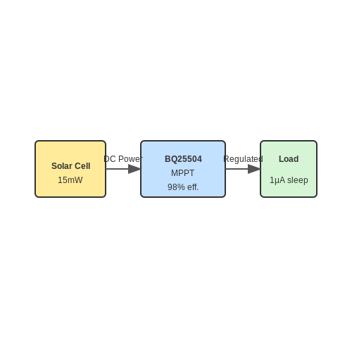
A practical implementation might use a 10cm2 photovoltaic cell (≈15mW in indoor lighting) with a TI BQ25504 power manager. The system achieves 1μA sleep current and 98% peak conversion efficiency by combining:
- Adaptive MPPT with 8-bit DAC resolution
- Hysteretic control for DC-DC conversion
- Programmable undervoltage lockout (UVLO) thresholds
4.3 Power-Aware Communication Protocols
Power-aware communication protocols optimize energy consumption in wireless and wired networks by dynamically adjusting transmission parameters such as modulation, coding, and packet size. These protocols are critical in battery-operated systems, IoT devices, and sensor networks where energy efficiency directly impacts operational lifetime.
Energy-Efficient Modulation Schemes
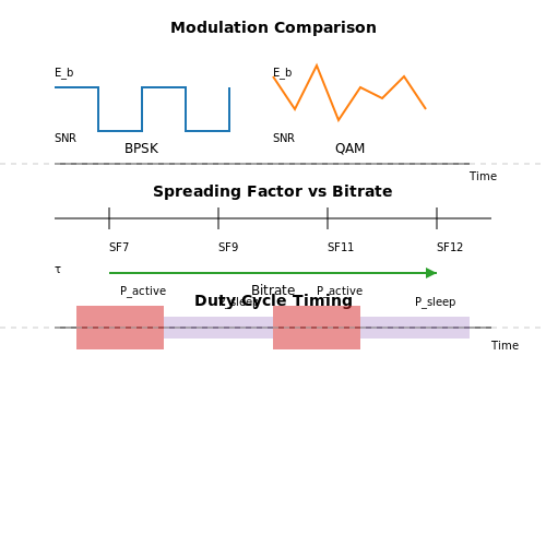
Modulation techniques influence power consumption due to their varying spectral efficiency and required signal-to-noise ratio (SNR). For instance, binary phase-shift keying (BPSK) consumes less power than quadrature amplitude modulation (QAM) at the cost of lower data rates. The energy per bit Eb can be derived as:
where Ptx is the transmit power and Rb is the bit rate. Lower-order modulations reduce Ptx but increase transmission time, necessitating a trade-off analysis.
Adaptive Data Rate Control
Protocols like IEEE 802.15.4 (Zigbee) and LoRaWAN employ adaptive data rate (ADR) algorithms to balance throughput and energy use. ADR adjusts spreading factors (SF) in LoRa based on link quality:
where B is bandwidth and Tsym is symbol duration. Higher SF values improve range but increase energy per bit.
Duty Cycling and Low-Power Listening
Duty cycling reduces idle listening by periodically activating transceivers. The power savings ΔP are modeled as:
where τ is the duty cycle ratio. Protocols like X-MAC and B-MAC optimize τ based on traffic patterns.
Packet Size Optimization
Larger packets reduce header overhead but increase retransmission energy in lossy channels. The optimal packet size Lopt minimizes total energy:
where p is the bit error rate, Eheader is header energy, and Ebit is per-bit transmission energy.
Case Study: Bluetooth Low Energy (BLE)
BLE’s power-aware features include:
- Connection Interval Adjustment: Ranges from 7.5 ms to 4 s, trading latency for energy savings.
- 1 Mbps Gaussian Frequency-Shift Keying (GFSK): Balances simplicity and moderate SNR requirements.
- Asymmetric Advertising: Reduces scan energy by allowing asymmetric advertisement intervals.
Empirical studies show BLE consumes 10–100× less energy than classic Bluetooth for intermittent data transfers.
Protocol Stack Optimization
Cross-layer designs merge physical, MAC, and routing layers to avoid redundant operations. For example, the Energy-Aware Routing Protocol (EARP) selects paths based on residual node energy:
where Eresidual,i is the remaining energy of node i in path N.
5. Key Research Papers in Low Power Design
5.1 Key Research Papers in Low Power Design
- Low Power Digital Design using Asynchronous Logic — the need for low power design. The demand for portable computers is increasing every year and is projected to increase in the future [1]. As consumers look for powerful yet low-power-consuming devices, there is a clear economic interest in the development of low power circuit design. The main reason behind the development of low power circuits ...
- PDF An Investigation of Low Power VLSI Design Techniques — Investigation of Low Power VLSI Design Techniques", Journal of Science, Computing and Engineering Research, 6(4), 05-09, 2023. I. INTRODUCTION The benefit of combining low-power components with low-power design strategies is more important than ever before. As components get smaller, more battery-powered,
- PDF Low Power VLSI Design Techniques: A Review - Journal of University of ... — Low Power VLSI Design Techniques: A Review Ketan J. Raut1*, Abhijit V. Chitre2, Minal S. Deshmukh3 and Kiran Magar4 1,2,3,4 Dept. of E&TC Engineering, Vishwakarma Institute of Information Technology, Pune, India 1 [email protected], 2 [email protected], 3 [email protected], [email protected] Abstract: Since CMOS technology consumes less power it is a key technology ...
- PDF Strategies & Methodologies for Low Power Vlsi Designs: a Review - Ijaet — paper describes about the various strategies, methodologies and power management techniques for low power circuits and systems. Future challenges that must be met to designs low power high performance circuits are also discussed. Keywords: Power Dissipation, low power, process nodes, leakage current, power management. 1. Introduction
- (PDF) Low Power Design Methodology - ResearchGate — Electronic Engineering; Low Power Design; Chapter PDF Available. Low Power Design Methodology. February 2018; February 2018; ... 1 5 1 C O U N T R I E S. A U T H O R S A M O N G. T O P 1 % M O S T ...
- Low power design for DSP: methodologies and techniques - Academia.edu — This paper provides an overview of these techniques and aims to serve as a bibliography of the key papers relevant to low power DSP design. Emphasis is given to aspects of design at higher levels due to their importance in reducing the 731 T. Arslan et al./Low power design for DSP overall design cost.
- Low Power VLSI Design Techniques: A Review - Academia.edu — Journal of University of Shanghai for Science and Technology ISSN: 1007-6735 Low Power VLSI Design Techniques: A Review Ketan J. Raut1*, Abhijit V. Chitre2, Minal S. Deshmukh3 and Kiran Magar4 1,2,3,4 1 Dept. of E&TC Engineering, Vishwakarma Institute of Information Technology, Pune, India [email protected], 2 [email protected], 3 ...
- Review Paper on Low Power VLSI Design Techniques - ResearchGate — Hence in modern low power VLSI design one of the major challenges is to design an efficient multiplier block. In this paper, a low power GDI based radix-4 modified Booth-Wallace multiplier has ...
- Strategies & Methodologies for Low Power Vlsi Designs: a Review — The paper is organized as follows: First, the sources of power dissipation in CMOS circuits and degrees of freedom in the low power design space are described in section-2. In section-3 various ...
- PDF LOW-POWER PROCESSOR DESIGN - Stanford University — short, as a measure of "goodness" for low-power designs. This chapter also describes the most common low-power techniques and explores how they affect the energy-delay product of CMOS circuits. Chapter 2 will show that exploiting parallelism is one important technique enabling the reduction of the energy-delay of a circuit.
5.2 Industry Standards and Benchmarks
- PDF IEC 61523-4:2023 - IEC 61523-4:2023 - iTeh Standards — Delay and power calculation standards - Part 4: Design and Verification of Low-Power, Energy-Aware Electronic Systems INTERNATIONAL ELECTROTECHNICAL COMMISSION ICS 25.040.01, 35.060 ISBN 978-2-8322-7540-5 Warning! Make sure that you obtained this publication from an authorized distributor. IEEE Std 1801™ ®
- PDF ©Rohde & Schwarz; Testing and optimizing low-power designs - IEEE Denver — LOW-POWER DESIGN CHALLENGE Low-power design generally starts with a low-power sys-tem concept, which means selecting the best-suited low-power communications technologies and components and utilizing their power-saving features. Most process-ing platforms and communications chips have different power modes: active, standby, sleep and deep sleep.
- PDF IEEE Standard for Design and Verification of Low Power Integrated Circuits — The purpose of this standard is to provide portable low power design specifications that can be used with a variety of commercial products throughout an electronic system design, analysis, verification, and implementation flow. When the electronic design automation (EDA) industry began creating standards for use in specifying,
- Designing Low-Power Circuits (LPCs) using an eFuse for Household and ... — 2 What are Low-Power Circuits (LPCs) The two standards, IEC60335-1 and UL 60730 have a lot in common including a shared definition of a Low-Power Circuit (LPC). The electronic circuit is a Low-Power Circuit as described below. "The control is operated at rated voltage or at the upper limit of the rated voltage range and a variable
- Low Power Methodology Manual - Synopsys — The "Low Power Methodology Manual" (LPMM) is a comprehensive and practical guide to managing power in system-on-chip designs, critical to designers using 90-nanometer and below technology.The authors, all low power experts, are led by Michael Keating, Synopsys Fellow and principal author of the widely adopted Reuse Methodology Manual for System-on-Chip Design, and David Flynn, ARM R&D Fellow ...
- PDF Design techniques for energy efficient and low-power systems - utwente.nl — dissipation at all levels of the design process. It was found that most low-power research is concentrated on components research: better batteries with more power per unit weight and volume; low-power CPUs; very low-power radio transceivers; low-power displays. We found that there is very little systems research on low-power systems.
- PDF Design Guidelines for Low Power Embedded Systems using Low Power ... — design specifications that must be met. Then, if at all feasible, choose the appropriate low-power components from Low Power Electronics (LPE). After studying and reviewing multiple LPES real-time projects, we compiled a list of a few strategies we may use to approach low-power design and consumption for embedded systems.
- PDF Design Methodologies and Strategies for Low Power VLSI — designing for low power adds another dimension to the already complex design problem and the design has to be optimized for power as well as Performance and Area. In conclusion various issues and major challenges regarding low power designs are:- 6.1 Technology Scaling: - It relates with the
- PDF Low Power Design Methodologies and Techniques: An Overview - Massoud Pedram — Low Power Design USC/LPCAD Page 6 USC Low Power CAD Massoud Pedram Power Dissipation Equations CMOS circuits only dissipate power when node voltages are changing V DD C P = CV DD fN +Q SC V DD fN + I leak V DD 0.5 2 f: frequency of clocking N: number of times gate switches in a clock cycle short circuit charge leakage current USC Low Power CAD ...
- Low-Power Design Advancements Supported by Emerging RF Standards ... — 3.3 Growth Restraints for the Low-Power IC Industry 3.4 Emerging Design Techniques in Low-Power ICs 3.5 Subthreshold Technology Overview and Patent Assessment of DVFS and Subthreshold Technologies
5.3 Recommended Books and Online Resources
- Practical Electronic Design for Experimenters - Default Book Series — Design Example 5.1 ; Design Example 5.2 ; Design Project 5.1 ; Design Project 5.2 ; Design Project 5.3 ; Design Project 5.4 ; Design Project 5.5 ; 6 Power Supply Design ; Power Supply Choices and Specifications ; The Make vs. Buy Decision ; Common Voltages ; Designing a Battery Supply ; Ampere-Hour Ratings ; Battery Supply Design Procedure ...
- Low-power electronics design : Free Download, Borrow, and Streaming ... — An illustration of an open book. Books. An illustration of two cells of a film strip. Video. An illustration of an audio speaker. Audio An illustration of a 3.5" floppy disk. ... Low-power electronics design. Publication date 2005 Topics Low voltage integrated circuits -- Design and construction, Low voltage systems -- Design and construction
- (PDF) Design for High Performance, Low Power, and Reliable 3D ... — We also began to look beyond the conventional TSV-based 3D ICs and started investigating monolithic 3D IC design. The 20 chapters included in this book are organized to reflect this evolution. The first part of this book contains six chapters on design issues and solutions for high performance and low power 3D ICs.
- MPG.eBooks - Staff View: Practical Low Power Digital VLSI Design — |a 1 Introduction -- 1.1 Needs for Low Power VLSI Chips -- 1.2 Charging and Discharging Capacitance -- 1.3 Short-circuit Current in CMOS Circuit -- 1.4 CMOS Leakage Current -- 1.5 Static Current -- 1.6 Basic Principles of Low Power Design -- 1.7 Low Power Figure of Merits -- 2 Simulation Power Analysis -- 2.1 SPICE Circuit Simulation -- 2.2 ...
- Best 25 books on VLSI Design — I n the previous article, Best 5 books have recommended for Physical Design Engineer. While writing that article it was very difficult to make many books out of the list. So I thought it will be better to write another article on the best 25 books for VLSI Design. This list starts from the basic level of books to the advance level of books.
- Portable Electronics: World Class Designs - 1st Edition - Elsevier Shop — The result is a book covering the gamut of electronic design from design fundamentals to low-power approaches with a strong pragmatic emphasis. In addition to specific design techniques and practices, this book also discusses various approaches to solving electronic design problems and how to successfully apply theory to actual design tasks ...
- PDF DESIGNING EMBEDDED PROCESSORS - content.e-bookshelf.de — 2.1 Power vs. Energy 289 2.2 Power/Energy vs. Performance 292 2.3 Power/Energy vs. Temperature 295 2.4 Summary 296 3. Future Compiler Research Directions 297 4. Techniques Covered in Subsequent Chapters 298 4.1 Dynamic Voltage and Frequency Scaling 298 4.2 Resource Hibernation 299 4.3 Remote Task Mapping 299 References 300 14
- Low Power Design - O'Reilly Media — Low Power Design There are several ways you can reduce the power consumption in your embedded system. The use of low-power devices is the most obvious place to start. The … - Selection from Designing Embedded Hardware, 2nd Edition [Book]
- Architectural Techniques for Low Power | SpringerLink — 6.7.2 Coarse-Grain and Fine-Grain Power Gating. The description in this book has mainly focused on power domains where a block of logic has a common power supply which can be switched off using the power switches. Such a set up is called coarse-grain power gating since the power switch cells control the power supply for a block of logic. The ...
- PDF Low Power Methodology Manual - download.e-bookshelf.de — Low Power Methodology Manual For System-on-Chip Design Robert Aitken Alan Gibbons• • Kaijian Shi Michael Keating • David Flynn •