Sputtering Techniques in Thin-Film Deposition
1. Principles of Sputtering
Principles of Sputtering
Physical Mechanism of Sputtering
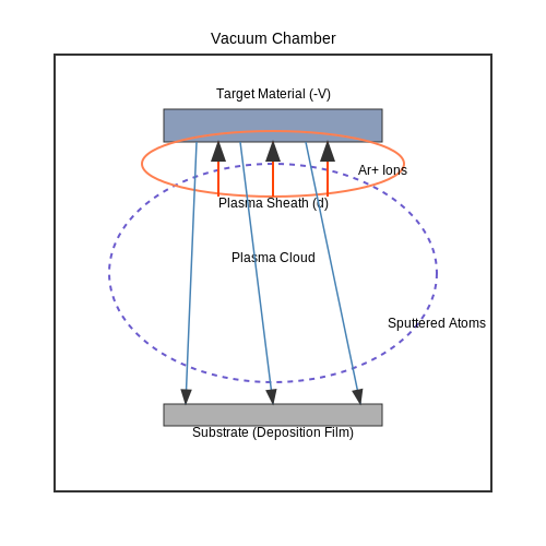
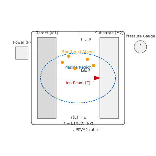
Sputtering is a physical vapor deposition (PVD) process where atoms are ejected from a solid target material due to bombardment by energetic ions, typically noble gas ions like Ar+. The process occurs in a vacuum chamber where a plasma is generated, creating positively charged ions that accelerate toward the negatively biased target.
The sputtering yield Y, defined as the number of target atoms ejected per incident ion, is given by:
where α is a dimensionless factor depending on the mass ratio m1/m2 (ion to target atom), Sn(E) is the nuclear stopping cross-section, U0 is the surface binding energy, and θ is the angle of incidence.
Energy Transfer Dynamics
The energy transfer between the incident ion and target atom follows a binary collision model. The maximum energy transfer fraction γ is:
For efficient sputtering, the ion energy must exceed the target material's threshold displacement energy (typically 20-50 eV). The most effective sputtering occurs when m1 ≈ m2, explaining why argon (atomic weight 40) is commonly used for sputtering metals like aluminum (27) or copper (64).
Plasma-Target Interactions
The plasma sheath forms at the target surface, creating a potential drop that accelerates ions toward the target. The sheath thickness d follows the Child-Langmuir law:
where J is the ion current density, V is the applied voltage, M is the ion mass, and e is the electron charge. This equation determines the ion flux uniformity across the target.
Angular and Energy Distribution
Sputtered atoms follow a modified cosine distribution with a preferential forward direction at higher ion energies. The energy distribution peaks at approximately half the surface binding energy U0, with a high-energy tail extending to several eV.
Practical Considerations
- Target poisoning: Reactive gases can form compounds on the target surface, altering sputtering yields
- Thermal management: High-power applications require active cooling to prevent target melting
- Step coverage: Sputtered films exhibit poorer conformality compared to chemical vapor deposition
The deposition rate R can be estimated from the sputtering yield:
where n0 is the atomic density of the target material and J is the ion current density.
1.2 Types of Sputtering Processes
DC Sputtering (Diode Sputtering)
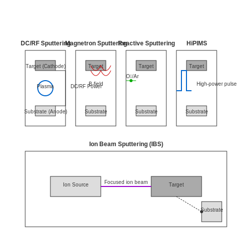
DC sputtering, the simplest form of sputter deposition, employs a direct current (DC) power supply to generate a plasma between a cathode (target) and anode (substrate). Argon ions, accelerated by the electric field, bombard the target, ejecting atoms that deposit onto the substrate. The process operates at pressures typically between 1–100 mTorr, with discharge voltages ranging from 500–5000 V. A key limitation is its restriction to conductive targets, as insulating materials accumulate charge, leading to arcing and process instability.
Here, J is the ion current density, ne the electron density, e the elementary charge, Vdc the applied voltage, and mi the ion mass. DC sputtering is widely used for metallic coatings in microelectronics, such as aluminum interconnects.
RF Sputtering
Radio-frequency (RF) sputtering overcomes DC limitations by applying an alternating current (typically 13.56 MHz) to the target. The high-frequency oscillation prevents charge buildup on insulating targets, enabling the deposition of dielectrics like SiO2 or Al2O3. The self-bias voltage (Vdc) that develops on the target is given by:
where PRF is the RF power, A the electrode area, and f the frequency. RF sputtering achieves lower deposition rates (~50% of DC) due to energy losses in capacitive coupling but is indispensable for oxide thin films in optical coatings.
Magnetron Sputtering
Magnetron sputtering enhances efficiency by trapping electrons near the target using permanent magnets, increasing ionization density. The magnetic field strength (B) follows:
where μ0 is permeability, N coil turns, I current, and r radius. This configuration reduces operating pressures to 0.1–10 mTorr, minimizing gas scattering and improving film density. Balanced/unbalanced magnetron designs trade off between deposition rate uniformity and ion bombardment intensity, critical for hard coatings like TiN.
Reactive Sputtering
In reactive sputtering, a reactive gas (e.g., O2, N2) is introduced alongside argon, forming compound films (e.g., TiO2, TiN) through surface reactions. The process exhibits hysteresis in the Q (reactive gas flow) vs. P (target poisoning) curve:
Here, θ is the target coverage fraction, S0 and S1 sticking coefficients, and α, β reaction constants. Precise control via plasma emission monitoring (PEM) is essential to avoid unstable transition regions.
High-Power Impulse Magnetron Sputtering (HiPIMS)
HiPIMS employs short (50–200 μs), high-power (>1 kW/cm2) pulses to generate ultra-dense plasmas (ne > 1019 m−3). The peak current density (jpeak) scales as:
where Upulse is pulse voltage and d target-substrate distance. HiPIMS produces films with exceptional adhesion (e.g., CrN for cutting tools) due to intense ion bombardment (ion-to-neutral ratios >50%), albeit at reduced deposition rates (~30% of DC).
Ion Beam Sputtering (IBS)
IBS decouples plasma generation and sputtering by using a separate ion source (typically Kaufman-type) to direct a focused beam (0.5–2 keV) at the target. The sputter yield Y follows Sigmund’s theory:
where m1, m2 are projectile/target masses, E ion energy, and U0 surface binding energy. IBS achieves sub-nanometer roughness, making it ideal for laser mirror coatings (e.g., Ta2O5/SiO2 multilayers).
1.3 Key Parameters in Sputtering
1.3.1 Sputtering Yield
The sputtering yield Y quantifies the number of target atoms ejected per incident ion. It depends on:
- Ion energy (typically 100–1000 eV)
- Ion mass and target mass ratio
- Binding energy of target atoms
- Incident angle of ions
where α is a dimensionless factor (0.1–0.5), Sn(E) is the nuclear stopping cross-section, U0 is the surface binding energy, and M1, M2 are the masses of incident ion and target atom respectively.
1.3.2 Pressure and Mean Free Path
Working gas pressure (typically 1–10 mTorr for DC sputtering) affects:
- Plasma density (higher pressure increases ionization)
- Mean free path λ of sputtered atoms
where d is the collision diameter (~3 Å for Ar), P is pressure, and T is gas temperature. Lower pressure increases λ but reduces deposition rate.
1.3.3 Substrate Temperature Effects
Substrate temperature Ts influences film properties through:
- Surface diffusion coefficient Ds:
Higher Ts promotes crystalline growth but may cause interdiffusion at interfaces.
1.3.4 Power and Bias Voltage
RF power (13.56 MHz) or DC power controls:
- Plasma density (∝ power input)
- Ion bombardment energy
Substrate bias voltage Vb modifies film stress and density:
- Positive bias: Reduces compressive stress
- Negative bias: Increases density but may induce defects
1.3.5 Target-to-Substrate Distance
Optimal distance balances:
- Deposition uniformity (longer distance improves uniformity)
- Deposition rate (shorter distance increases rate)
- Resputtering effects (closer spacing increases ion bombardment)
Typical distances range from 50–150 mm in industrial systems.
1.3.6 Gas Composition
Reactive sputtering uses gas mixtures (e.g., Ar + O2 for oxides):
- Poisoning regime: Target surface reacts with gas
- Metallic regime: Insufficient reactive gas
The hysteresis effect occurs in reactive sputtering where small gas flow changes cause abrupt transitions between regimes.
2. DC Sputtering: Mechanism and Applications
2.1 DC Sputtering: Mechanism and Applications
Fundamental Principles
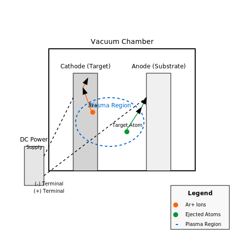
DC sputtering, or direct current sputtering, is a physical vapor deposition (PVD) technique where a DC power supply generates a plasma discharge in a low-pressure inert gas environment (typically Argon). The target material, serving as the cathode, is bombarded by energetic ions from the plasma, ejecting atoms that subsequently deposit onto a substrate. The process relies on the following key phenomena:
- Plasma Generation: A voltage (typically 500–1000 V) ionizes the inert gas, creating a glow discharge.
- Momentum Transfer: Ar+ ions accelerate toward the cathode, dislodging target atoms via kinetic energy transfer.
- Deposition: Ejected atoms travel ballistically and condense on the substrate.
Mathematical Framework
The sputtering yield Y, defined as the number of target atoms ejected per incident ion, is derived from Sigmund's theory:
where:
- α is a material-dependent constant,
- Sn(E) is the nuclear stopping power,
- U0 is the surface binding energy,
- θ is the ion incidence angle.
System Configuration
A basic DC sputtering system comprises:
- Vacuum Chamber: Maintains pressures of 1–100 mTorr.
- Target: Conductive material (e.g., Al, Cu, ITO) bonded to the cathode.
- Substrate Holder: Electrically floating or biased, positioned opposite the target.
- DC Power Supply: Delivers constant voltage/current, sustaining the plasma.
Process Limitations
DC sputtering is restricted to conductive targets due to:
- Charge Accumulation: Insulating materials develop surface charges, quenching the plasma.
- Arcing: Localized dielectric breakdowns cause particulate contamination.
Industrial Applications
Widely used for depositing:
- Metallization Layers: Aluminum interconnects in ICs, copper seed layers.
- Transparent Conductive Oxides (TCOs): Indium tin oxide (ITO) for displays.
- Magnetic Films: NiFe alloys for read/write heads.
Case Study: ITO Deposition
For optoelectronic devices, DC sputtering achieves:
- Resistivity: 1–3 × 10⁻⁴ Ω·cm at 90% transparency.
- Uniformity: ±3% thickness variation across 200 mm wafers.
2.2 RF Sputtering: Advantages and Limitations
Fundamentals of RF Sputtering
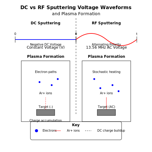
RF sputtering employs radio frequency (RF) power, typically at 13.56 MHz, to generate plasma in a vacuum chamber. Unlike DC sputtering, which requires a conductive target, RF sputtering can deposit both conductive and insulating materials due to its alternating electric field. The RF signal oscillates at a frequency high enough to prevent charge buildup on insulating targets, enabling sustained plasma discharge.
where VRF is the applied RF voltage, V0 is the peak voltage, and f is the frequency (13.56 MHz). The self-bias voltage (VDC) that develops on the target due to asymmetric electrode geometry is given by:
where Acathode and Aanode are the surface areas of the target and grounded electrode, respectively.
Advantages of RF Sputtering
- Deposition of insulating materials: RF sputtering avoids charge accumulation on non-conductive targets (e.g., Al2O3, SiO2), enabling uniform film growth.
- Lower operating pressures: The high ionization efficiency of RF plasma allows deposition at pressures as low as 1–10 mTorr, reducing gas incorporation in films.
- Better step coverage: The alternating field enhances plasma density, improving conformal coating of high-aspect-ratio structures.
- Reduced arcing: The absence of continuous DC voltage minimizes arcing, critical for sensitive semiconductor applications.
Limitations and Challenges
- Lower deposition rates: RF sputtering typically achieves 30–50% lower rates than DC sputtering due to lower ion current densities.
- Complex impedance matching: RF systems require impedance matching networks to maximize power transfer, adding complexity and cost.
- Substrate heating: The high-frequency field increases ion bombardment energy, raising substrate temperatures (often >200°C).
- Target utilization: Non-uniform erosion patterns ("racetrack") reduce target material usage efficiency to ~30%.
Practical Applications
RF sputtering is indispensable in depositing dielectric layers for optical coatings (e.g., anti-reflective MgF2), piezoelectric films (ZnO, AlN), and diffusion barriers (Si3N4) in microelectronics. Recent advances in pulsed RF sputtering have enabled high-quality ferroelectric films (e.g., PZT) for MEMS devices.
2.3 Comparison of DC and RF Sputtering
Fundamental Operating Principles
DC sputtering relies on a continuous direct current (DC) power supply to generate a plasma discharge. The target material, acting as the cathode, is bombarded by Ar+ ions, leading to the ejection of atoms via momentum transfer. The process requires the target to be electrically conductive to sustain the discharge. In contrast, RF sputtering employs an alternating current (typically at 13.56 MHz) to create a time-varying electric field, enabling the formation of a plasma even with insulating targets. The rapid polarity reversal prevents charge accumulation on non-conductive surfaces.
Plasma Characteristics and Ionization Efficiency
DC plasmas exhibit lower ionization densities (~109–1010 cm−3) compared to RF plasmas (~1010–1011 cm−3). The RF electric field enhances electron acceleration through stochastic heating, increasing the probability of inelastic collisions with neutral gas molecules. This results in higher deposition rates for RF sputtering at equivalent power levels. However, DC plasmas provide more directional ion bombardment due to the constant electric field orientation.
Target Material Compatibility
- DC Sputtering: Limited to conductive materials (metals, doped semiconductors). Insulators accumulate surface charge, terminating the discharge.
- RF Sputtering: Compatible with all materials, including ceramics (Al2O3, SiO2) and polymers. The AC field prevents charge buildup.
Process Parameters and Control
DC systems operate at lower voltages (300–500 V) but higher currents (1–10 A), while RF systems use high voltages (500–2000 Vpp) at lower currents (0.1–1 A). Impedance matching is critical in RF sputtering to maximize power transfer, requiring a matching network with variable capacitors. The self-bias voltage (Vdc) in RF sputtering follows:
Deposition Rate and Film Quality
For metallic targets, DC sputtering achieves higher deposition rates (100–1000 nm/min) due to greater ion flux. RF sputtering typically yields 10–100 nm/min but produces denser films with fewer defects, attributed to higher energy ions and better substrate heating. Stress control is superior in RF mode, making it preferable for MEMS and optical coatings.
Industrial Applications
- DC Sputtering: Metallization in semiconductors, reflective coatings, and low-resistivity interconnects.
- RF Sputtering: Dielectric layers (SiO2, Si3N4), piezoelectric films (ZnO, AlN), and transparent conductive oxides (ITO).
Economic and Operational Considerations
DC systems have lower capital costs (~$$50k–$$100k) and simpler maintenance. RF systems are more expensive (~$$150k–$$300k) due to the RF generator and matching network complexity. However, RF offers longer target lifetimes by reducing arcing and uneven erosion.
3. Working Principle of Magnetron Sputtering
3.1 Working Principle of Magnetron Sputtering
Magnetron sputtering is a plasma-based physical vapor deposition (PVD) technique that utilizes crossed electric and magnetic fields to enhance sputtering efficiency. The process begins with the ionization of a sputtering gas, typically argon, in a vacuum chamber held at pressures between 0.1–10 Pa. A negative bias voltage (typically -200 to -1000 V) is applied to the target material, creating a glow discharge plasma.
Plasma Confinement and Electron Trapping
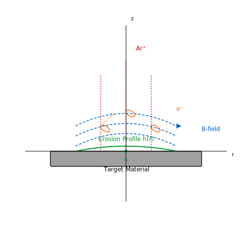
The key innovation in magnetron sputtering is the use of permanent magnets or electromagnets arranged behind the target to generate a closed-loop magnetic field parallel to its surface. This field confines secondary electrons emitted from the target into spiral trajectories along the field lines, described by the electron cyclotron motion equation:
where re is the electron gyroradius, me is electron mass, v⊥ is velocity perpendicular to the magnetic field B, and e is electron charge. This confinement increases the electron path length by several orders of magnitude, dramatically boosting ionization probability.
Sputtering Yield Enhancement
The trapped electrons ionize additional argon atoms through collisions, creating a high-density plasma region (1016–1018 m-3) near the target surface. The resulting Ar+ ions are accelerated toward the target by the electric field, with their impact energy given by:
The sputtering yield Y follows Sigmund's theory:
where α is a mass-dependent factor, Sn(E) is the nuclear stopping power, U0 is surface binding energy, Eth is threshold energy, and θ is incidence angle.
Erosion Profile and Target Utilization
The magnetic field configuration creates a racetrack-shaped erosion pattern on the target. The depth profile h(r) follows:
where r0 is the racetrack center position and σ characterizes erosion width. Typical target utilization ranges from 20–40%, with unbalanced magnetron designs achieving up to 60%.
Process Advantages
- High deposition rates (0.1–10 nm/s) compared to conventional sputtering
- Lower operating pressures reduce gas incorporation in films
- Reduced substrate heating from electron bombardment
- Excellent stoichiometry control for compound materials
Modern implementations often employ pulsed DC or RF power for insulating targets, with high-power impulse magnetron sputtering (HiPIMS) achieving peak power densities exceeding 1 kW/cm2 for enhanced ionization.
3.2 Balanced vs. Unbalanced Magnetron Sputtering
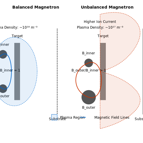
Magnetron sputtering systems are classified into balanced and unbalanced configurations based on the magnetic field topology. The distinction lies in the relative strengths of the inner and outer magnetic poles, which govern plasma confinement and ion bombardment efficiency.
Magnetic Field Configuration
In a balanced magnetron, the magnetic field lines form closed loops parallel to the target surface, confining electrons efficiently and enhancing ionization near the target. The plasma density peaks close to the target, limiting ion flux to the substrate. The magnetic field strength ratio between the outer and inner poles is typically close to unity:
In contrast, an unbalanced magnetron features a stronger outer pole, creating an extended magnetic field that projects toward the substrate. This configuration increases ion bombardment at the substrate by allowing more plasma to escape the target region. The field ratio is significantly greater than 1:
Plasma Characteristics
The plasma density distribution differs markedly between the two configurations:
- Balanced: High plasma density near the target (~1018 m-3), but rapid decay with distance. Ion current density at the substrate is typically 1-5 mA/cm2.
- Unbalanced: Lower peak density (~1017 m-3), but sustained density extending to the substrate. Ion current density can reach 10-50 mA/cm2.
Practical Implications
Balanced magnetrons excel in applications requiring:
- High deposition rates (up to 1 µm/min for metals)
- Minimal substrate heating
- Low-stress films (e.g., optical coatings)
Unbalanced magnetrons are preferred when:
- Enhanced ion bombardment is needed (e.g., for densification)
- Reactive sputtering of compounds (TiN, Al2O3)
- Substrate temperatures exceed 300°C
Energy Considerations
The ion energy distribution at the substrate follows:
where Vp is the plasma potential and Te the electron temperature. Unbalanced configurations typically exhibit broader distributions with higher mean energies (20-100 eV vs. 5-20 eV for balanced).
3.3 Applications in Thin-Film Deposition
Semiconductor Manufacturing
Sputtering is extensively used in semiconductor fabrication for depositing thin films of metals (e.g., aluminum, copper) and dielectrics (e.g., silicon dioxide, silicon nitride) onto silicon wafers. The technique enables precise control over film thickness and uniformity, critical for integrated circuits (ICs). For instance, copper interconnects in modern ICs rely on sputtering due to its ability to deposit high-purity, low-resistivity films with excellent step coverage.
Optical Coatings
In optical applications, sputtering deposits thin films with tailored refractive indices for anti-reflective coatings, mirrors, and filters. Multi-layer stacks of alternating high-index (e.g., TiO2) and low-index (e.g., SiO2) materials are fabricated using reactive sputtering. The process allows nanometer-scale precision, enabling applications in lenses, laser optics, and photovoltaic cells.
Magnetic Storage Media
Sputtering is pivotal in manufacturing hard disk drives (HDDs), where thin magnetic films (e.g., cobalt-chromium-platinum alloys) are deposited with high anisotropy and uniformity. The technique's ability to produce dense, defect-free films enhances data storage density. Additionally, giant magnetoresistance (GMR) read heads are fabricated using sputtered multi-layer structures.
Transparent Conductive Oxides (TCOs)
Indium tin oxide (ITO) films, widely used in touchscreens and flat-panel displays, are deposited via sputtering. The process achieves low resistivity (10−4 Ω·cm) and high transparency (>90%) by optimizing oxygen partial pressure during reactive sputtering. Alternatives like aluminum-doped zinc oxide (AZO) are also explored for cost reduction.
Decorative and Protective Coatings
Sputtering deposits wear-resistant coatings (e.g., TiN, CrN) on cutting tools and aerospace components. Decorative films (e.g., gold, titanium nitride) are applied to jewelry and architectural glass. The technique's versatility in material selection and adhesion strength makes it ideal for enhancing durability and aesthetics.
Energy Applications
Thin-film solar cells (e.g., CIGS, CdTe) utilize sputtering for absorber and buffer layers. The process enables large-area deposition with controlled stoichiometry, critical for photovoltaic efficiency. Similarly, sputtered lithium cobalt oxide (LiCoO2) films are used in solid-state batteries.
Emerging Applications
Recent advances include sputtering for 2D materials (e.g., graphene, MoS2) and flexible electronics. The technique's scalability and compatibility with roll-to-roll processing make it promising for next-generation wearable devices and IoT sensors.
where J is ion current density, A is target area, η is sputter yield, n is atomic density, and e is electron charge.
4. Process Overview and Chemical Reactions
4.1 Process Overview and Chemical Reactions
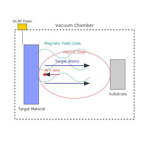
Sputtering is a physical vapor deposition (PVD) technique where atoms are ejected from a solid target material due to bombardment by high-energy ions, typically argon (Ar+). The ejected atoms then deposit onto a substrate, forming a thin film. The process occurs in a vacuum chamber under controlled pressure (typically 1–100 mTorr) with an applied DC or RF power supply to generate plasma.
Mechanism of Sputtering
The sputtering yield Y, defined as the number of target atoms ejected per incident ion, is governed by:
This yield depends on:
- Ion energy (typically 300–1000 eV)
- Ion mass (Ar+, Kr+, or Xe+)
- Target material's binding energy
- Angle of incidence
Chemical Reactions in Reactive Sputtering
In reactive sputtering, a reactive gas (e.g., O2, N2) is introduced to form compound films (e.g., oxides, nitrides). The key reactions include:
The reaction kinetics are influenced by:
- Partial pressure of reactive gas
- Plasma density
- Substrate temperature
Plasma Dynamics
The plasma discharge follows the Child-Langmuir law for ion current density J:
where V is the applied voltage, d is the cathode-anode distance, and mi is the ion mass.
Practical Considerations
In industrial applications, magnetron sputtering enhances deposition rates by confining electrons near the target using magnetic fields. This increases ionization efficiency, allowing operation at lower pressures (1–10 mTorr) while maintaining high sputtering yields.
4.2 Control of Reactive Gas Flow
Fundamentals of Reactive Gas Dynamics
In reactive sputtering, the introduction of reactive gases such as oxygen (O2) or nitrogen (N2) into the deposition chamber alters the chemical composition of the deposited film. The reaction kinetics between the sputtered metal atoms and the reactive gas molecules are governed by the partial pressure of the gas, which must be precisely controlled to achieve stoichiometric films. The reaction probability β is given by:
where kr and ks are the reaction and sputtering rate constants, respectively, and Pr and Ps are the partial pressures of the reactive gas and sputtering gas (typically argon).
Gas Flow Control Mechanisms
Precise regulation of reactive gas flow is achieved using:
- Mass Flow Controllers (MFCs): Provide closed-loop feedback control with accuracy up to ±0.5% of full scale. MFCs adjust gas flow based on thermal conductivity measurements.
- Pressure-Based Feedback Systems: Use capacitance manometers or Pirani gauges to dynamically adjust gas injection rates via proportional-integral-derivative (PID) algorithms.
- Plasma Emission Monitoring (PEM): Detects optical emission from excited species (e.g., atomic O at 777 nm) to maintain stoichiometry in real time.
The total gas flow Qtot is the sum of individual flows:
Hysteresis Effect and Process Stability
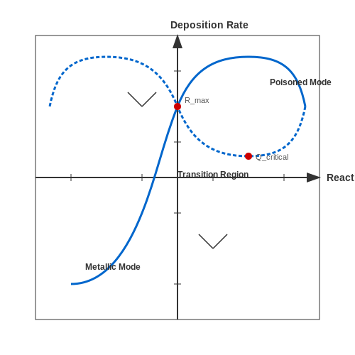
Reactive sputtering exhibits hysteresis in the deposition rate versus reactive gas flow curve due to target poisoning. The critical points are:
- Metallic Mode: Low reactive gas flow, high deposition rate, non-stoichiometric films.
- Transition Region: Unstable process with abrupt rate changes.
- Poisoned Mode: High reactive gas flow, low deposition rate, stoichiometric films.
The stability condition is derived from the balance between sputtering and reaction rates:
where θ is the fractional coverage of the target surface by reacted compounds.
Advanced Control Strategies
Modern systems employ:
- Pulsed Gas Flow: Modulates gas injection at kHz frequencies to suppress arcing in DC reactive sputtering.
- Plasma Impedance Matching: Adjusts RF power to compensate for impedance changes due to target poisoning.
- Machine Learning Optimization: Neural networks predict optimal gas flows based on historical process data.
For high-precision applications, the gas flow resolution must satisfy:
where δρ is the tolerable film property variation and ∂ρ/∂Q is the sensitivity of film density to gas flow changes.
4.3 Challenges and Solutions in Sputtering Techniques
Target Uniformity and Step Coverage
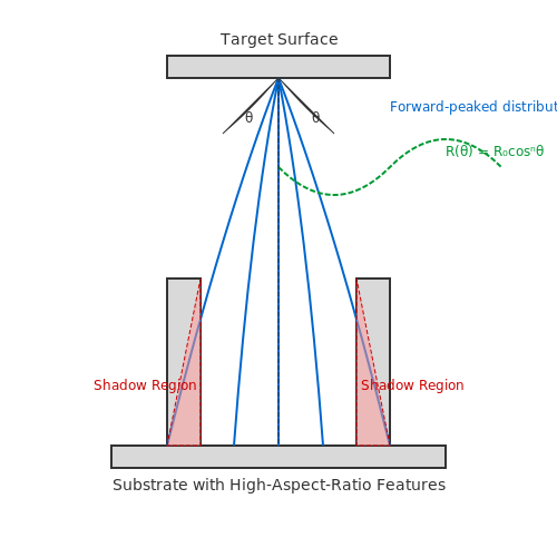
Achieving uniform film thickness across large-area substrates remains a persistent challenge in sputtering, particularly for non-planar geometries. The deposition rate R varies with the emission angle θ of sputtered atoms following a modified cosine distribution:
where n > 1 indicates forward-peaked distributions common in magnetron sputtering. This results in shadowing effects at high aspect-ratio features. Solutions include:
- Rotating substrate holders with planetary motion systems
- Collimated sputtering using honeycomb filters (30-50% thickness variation reduction)
- Long-throw sputtering at target-to-substrate distances >300 mm
Particle Contamination and Arcing
Micro-arcs at the target surface generate particulate defects (>0.3 μm) that degrade film quality. The arcing frequency f follows:
where Vdc is the cathode voltage and Te the electron temperature. Modern approaches combat this through:
- Pulsed DC power supplies (100-350 kHz) with arc suppression circuits (<1 μs response)
- Reactive gas flow control algorithms maintaining 10-3 Torr stability
- Target preconditioning protocols using controlled arcing
Stress Control in Deposited Films
Intrinsic stress σ in sputtered films arises from atomic peening effects and thermal expansion mismatch:
where E is Young's modulus, ν Poisson's ratio, and ΔV/V0 the volumetric strain. Stress management techniques include:
- Bias sputtering with -50V to -200V substrate bias
- Post-deposition annealing at 0.3-0.5 Tmelt (film material)
- Multilayer architectures with alternating compressive/tensile layers
Process Reproducibility
Run-to-run variations exceeding ±5% in resistivity or stoichiometry often stem from:
- Target erosion profiles changing emission characteristics
- Poisoning state instability in reactive sputtering
- Residual gas composition fluctuations
Advanced solutions incorporate:
- Real-time plasma impedance monitoring with 100 ms resolution
- Machine learning-based process control (neural networks trained on 104+ deposition runs)
- Rotating cylindrical targets with uniform erosion
High-κ Dielectric Challenges
For materials like HfO2 or Al2O3, key issues include:
- Oxygen deficiency leading to leakage currents >10-6 A/cm2
- Metallic contamination from target impurities
- Interfacial layer formation during deposition
Mitigation strategies involve:
- Radical-enhanced sputtering with remote O2 plasma
- Ultra-high purity targets (99.9995%) with getter sputtering
- In-situ XPS monitoring of oxidation states
5. Ion Beam Sputtering: Precision and Control
5.1 Ion Beam Sputtering: Precision and Control
Fundamentals of Ion Beam Sputtering
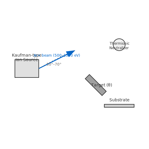
Ion beam sputtering (IBS) employs a focused beam of high-energy ions (typically Ar+ at 500–1500 eV) to eject target material atoms via momentum transfer. Unlike conventional sputtering, where plasma-generated ions bombard the target, IBS decouples ion generation from the deposition process, enabling independent control of ion energy, flux, and incidence angle. The sputter yield Y follows Sigmund's theory:
where α is a material-dependent constant, Sn(E) is the nuclear stopping power, U0 is the surface binding energy, and f ≈ 2.5 for most materials.
System Configuration
A typical IBS system comprises:
- Ion source: Kaufman-type or RF inductively coupled plasma (ICP) source generating 1–3 cm diameter beams with current densities of 1–10 mA/cm2.
- Neutralizer: Electron emitter (e.g., thermionic filament) to prevent charge buildup on insulating targets.
- Target-substrate geometry: Configurable angles (30°–70°) between ion beam, target, and substrate to tune film properties.
Energy and Angular Distribution
Ejected atoms follow a modified cosine distribution with a forward-peaking component due to collision cascades. The energy distribution peaks at 1–10 eV, described by:
This results in higher adatom mobility compared to thermal evaporation, promoting dense film growth.
Advantages Over DC/RF Sputtering
- Lower operating pressure: 10−4–10−2 mTorr reduces gas incorporation and scattering losses.
- Precise stoichiometry control: Independent target bombardment enables co-sputtering of multiple materials with sub-nm thickness resolution.
- Reduced substrate heating: Absence of plasma near the substrate minimizes thermal damage to sensitive materials.
Applications in High-Precision Coatings
IBS excels in depositing:
- Ultra-low loss optical coatings (SiO2/Ta2O5 multilayers with Δn/n < 10−4)
- Magnetic tunnel junctions (CoFeB/MgO interfaces with >200% TMR)
- Topological insulator films (Bi2Se3 with < 0.1 nm roughness)
Challenges and Mitigations
Key limitations include:
- Low deposition rates: Typically 0.01–0.1 nm/s, addressed by multi-beam configurations.
- Ion-induced damage: Optimized beam energies below displacement thresholds (e.g., <50 eV for Si).
- Uniformity constraints: Requires raster scanning or rotating substrate holders for large-area coatings.
Recent Advances
Dual-ion-beam systems now incorporate:
- Assist beams (5–30 eV) for in-situ densification
- Reactive oxygen/nitrogen beams for oxide/nitride synthesis
- Mass-separated beams for isotopic purity (e.g., 28Si vs 30Si)
5.2 Pulsed DC and HiPIMS Techniques
Pulsed DC Sputtering
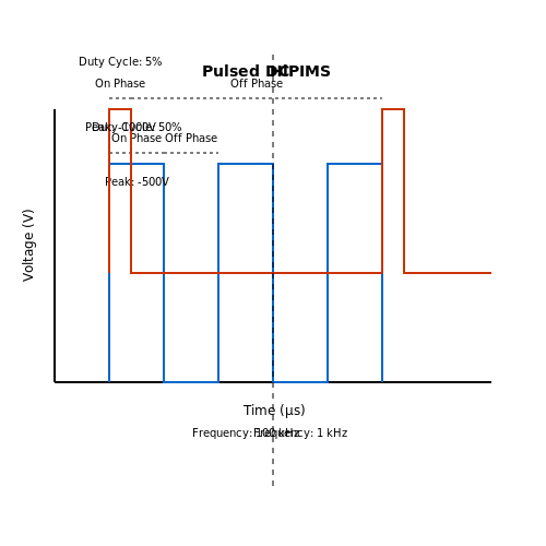
Pulsed DC sputtering modifies conventional DC sputtering by applying a time-modulated voltage instead of a continuous DC signal. This technique mitigates arcing and target poisoning—common issues in reactive sputtering—by periodically reversing the polarity of the applied voltage. The pulsing frequency typically ranges from 10 kHz to 350 kHz, with duty cycles between 30% and 90%. The voltage reversal during the off-phase neutralizes charge buildup on insulating layers, enabling stable deposition of dielectric materials like Al2O3 or SiO2.
Here, V0 is the peak voltage, τ the pulse width, and f the frequency. The average power delivered to the plasma is:
High-Power Impulse Magnetron Sputtering (HiPIMS)
HiPIMS operates by applying ultra-high power pulses (kW/cm2) at low duty cycles (<10%), creating a highly ionized plasma. The peak current densities exceed 1 A/cm2, resulting in 90% ionization rates for metallic species. This enables precise control over film microstructure, adhesion, and density through substrate bias tuning. Key parameters include:
- Pulse duration: 50–200 μs
- Peak power density: 1–3 kW/cm2
- Repetition rate: 100–1000 Hz
Plasma Dynamics in HiPIMS
The ionization process follows a self-sputtering runaway mechanism. Initially, gas ions (Ar+) sputter target material, which then becomes ionized (M+) and contributes to further sputtering. The ion flux Γi at the substrate is given by:
where ni is ion density, Te electron temperature, and mi ion mass. The ion-to-neutral ratio can exceed 10:1, enabling epitaxial growth at lower temperatures.
Applications and Comparative Advantages
Pulsed DC is preferred for reactive deposition of oxides/nitrides, while HiPIMS excels in:
- Dense, pinhole-free coatings for aerospace components
- Low-temperature growth of crystalline films (e.g., TiO2 rutile phase)
- High-aspect-ratio trench filling in semiconductor interconnects
5.3 Emerging Trends in Sputtering Technology
High-Power Impulse Magnetron Sputtering (HiPIMS)
High-Power Impulse Magnetron Sputtering (HiPIMS) has emerged as a breakthrough in thin-film deposition, offering superior ionization rates compared to conventional DC magnetron sputtering. By applying short, high-power pulses (typically 1–10 kW/cm² at 100–500 Hz), HiPIMS generates a dense plasma with a high fraction of ionized sputtered species. The ionization fraction α can be derived from the plasma density ne and electron temperature Te:
where ni is the ion density, n0 the neutral density, ⟨σv⟩ the ionization rate coefficient, and L the plasma length. HiPIMS enables precise control over film microstructure, enhancing adhesion and density in applications like wear-resistant coatings and semiconductor interconnects.
Reactive Sputtering with Closed-Loop Control
Reactive sputtering of compound films (e.g., Al2O3, TiN) traditionally suffers from hysteresis effects, leading to process instability. Modern systems now employ closed-loop control using optical emission spectroscopy (OES) or plasma impedance monitoring to regulate reactive gas flow in real time. The feedback loop adjusts the O2 or N2 partial pressure to maintain stoichiometry, governed by:
where Kp and Ki are PID constants, and e(t) is the error signal from the OES detector. This method is critical for depositing high-quality dielectric layers in optical coatings and MEMS devices.
Energy-Driven Sputtering
Recent advances focus on tailoring the energy distribution of sputtered atoms. Techniques like ion-beam-assisted deposition (IBAD) and biased target deposition (BTD) allow direct control over adatom mobility. In BTD, a negative bias (Vb = −50 to −200 V) applied to the target increases ion bombardment energy, modifying film stress and crystallinity. The energy flux Φ to the substrate follows:
where jion is the ion current density and ηenergy the energy transfer efficiency. This approach is pivotal for growing epitaxial films in quantum dot devices and superconducting layers.
Hybrid Sputtering-PECVD Systems
Combining sputtering with plasma-enhanced chemical vapor deposition (PECVD) enables co-deposition of metallic and polymeric phases. For example, Ag-embedded SiO2-C films for antibacterial surfaces are synthesized by simultaneously sputtering Ag while injecting hexamethyldisiloxane (HMDSO) precursor gas. The hybrid process requires balancing the sputtering yield Y and the PECVD deposition rate Rd:
Machine Learning for Process Optimization
Neural networks are being trained on sputtering datasets to predict film properties (e.g., roughness, resistivity) from process parameters (power, pressure, substrate temperature). A typical model uses a 3-layer perceptron with input features normalized to dimensionless groups like the S* parameter (normalized sputtering rate):
where λmean is the mean free path and Aerosion the target erosion area. Such models reduce trial-and-error in industrial coating production.
6. Key Research Papers and Reviews
6.1 Key Research Papers and Reviews
- Handbook of Thin Film Deposition Processes and Techniques (2) — 1993. The Institute was divided in four sessions which included comprehensive reviews and di focused on four main subjects as described below: (1) Descriptions and discussions of thin film deposition techniques (plasma and ion beam sputtering systems, systems and basic principles of chemical vapor deposition, physics and chemistry of film growth from the vapor phase, and molecular beam epitaxy ...
- Thin Film Deposition and Nanoscale Characterisation Techniques - Springer — In this chapter the basic categories of the thin film deposition techniques are presented. The rf magnetron sputtering (MS) deposition conditions and their effect to the optical, nanostructural and nanomechanical properties of: (a) single layer and multilayer, hard and soft carbon-based thin films grown on rigid Si substrate and (b) AlO x thin films grown on flexible polyethylene terephthalate ...
- PDF Thin Film Deposition and Nanoscale Characterisation Techniques — (CVD) [3], and the Wet deposition techniques. In Fig. 6.1 the thin film deposition techniques as well as their subcategories are presented. In the following paragraphs we focus on thin films deposited by using Physical Vapor Deposition, and Wet deposition techniques. In the case of the PVD the discussion centers at the magnetron sputtering of ...
- Atomic layer deposition and other thin film deposition techniques: from ... — Several reviews on deposition techniques have been reported [[25], ... thin films by DC reactive magnetron sputtering method to probe the electronic, electrical, and optical properties. The films were deposited on a glass substrate at 573-623 K with film thickness and grain sizes ranging from 400 to 500 nm and 120-220 nm, respectively ...
- Full article: State-of-the-art electrochromic thin films devices ... — The sputtering deposition can be applied as a generic term encompassing several procedures such as bias sputtering, diode sputtering (cathode or radio frequency), ion-beam sputtering, reactive sputtering, and magnetron sputtering [Citation 103, Citation 104] based on source and method. Variations in working pressure bring about by the power ...
- Growth and Properties of Magnetic Thin Films using Magnetron — outstanding mentorship throughout my graduate research career. Next, I would like to thank Prof. Jiwei Lu for professional guidanchis e at the initial stage of my research, and the stimulating discussion and advices throughout my whole graduate research period. I would like to thank all of the former and present members my research group, in
- Effects of film thickness and sputtering power on properties of ITO ... — Usually, ITO thin-film structures are deposited by well-known magnetron sputtering techniques [26][27][28][29]. The variation of sputtering conditions (working gas pressure and mixture, sputtering ...
- Thin Film Deposition Techniques: A Comprehensive Review - ResearchGate — The synthesis of these techniques illustrates the dynamic landscape of thin film technology, underlining its critical role in future innovations. Discover the world's research 25+ million members
- Basic deposition methods of thin films - ScienceDirect — A layer of thin film on the substrate surface is formed in short interval of time. However, this technique is not suited for insulating targets as it causes ion accumulation on target surface. Figure. 12 shows the schematic diagram of the DC-sputtering deposition technique.
- Sputter Deposition Processes - ScienceDirect — Two approaches can be followed to produce ions and sputter the target materials. The first is quite straightforward by using an ion source which is aimed toward the target. Collecting the sputtered particles on a substrate enables the deposition of a thin film. However, ion beam sputtering is not widely used for industrial large-scale applications.
6.2 Recommended Textbooks and Manuals
- Handbook of Sputter Deposition Technology - 2nd Edition - Elsevier Shop — 5. Basic Process of Sputtering Deposition. 5.1 Control of Film Quality. 5.2 Reactive Sputtering- 5.3 Typical Deposition Conditions of Functional Thin Films. References. 6. Functional Thin Films. 6.1 ZnO Thin Films. 6.2 Compound Oxide Thin Films. 6.3 Nitrides, Carbides, Silicates, Selenides. 6.4 Amorphous Thin Films. 6.5 Miscellaneous ...
- Handbook of Thin Film Deposition - 5th Edition - Elsevier Shop — Handbook of Thin Film Deposition: Theory, Technology and Semiconductor Applications, Fifth Edition, is a comprehensive reference focusing on thin film technologies and applications used in the semiconductor industry and the closely related areas of thin film deposition, thin film microproperties, ferroelectric films, LED research, and materials for memory applications, and other thin film ...
- PDF Handbook of Thin-film Deposition Processes and Techniques - Icdst — Handbook of Thin-Film Deposition Processes and Techniques / [edited] by Krishna Seshan. -- 2nd edition p. cm. Includes bibliographical references and index. ISBN -8155-1442-5 1. Thin film devices -- Design and construction -- Handbooks, manuals, etc. I. Seshan, Krishna. II. Title. TK7872.T55H36 2001135178 621.381'72--dc19 CIP NOTICE
- Handbook of Thin Film Deposition Techniques Principles Methods ... - Scribd — The document promotes the 'Handbook of Thin Film Deposition Techniques' by Krishna Seshan, providing links to download the book and other related ebooks on thin film technology. It highlights the evolution of thin film deposition processes in semiconductor manufacturing and their applications across various industries. The second edition includes updated information reflecting recent ...
- Thin Film Deposition and Nanoscale Characterisation Techniques - Springer — In this chapter the basic categories of the thin film deposition techniques are presented. The rf magnetron sputtering (MS) deposition conditions and their effect to the optical, nanostructural and nanomechanical properties of: (a) single layer and multilayer, hard and soft carbon-based thin films grown on rigid Si substrate and (b) AlO x thin films grown on flexible polyethylene terephthalate ...
- PDF Thin Film Deposition and Nanoscale Characterisation Techniques — Vapor Deposition, and Wet deposition techniques. In the case of the PVD the discussion centers at the magnetron sputtering of carbon-based thin films, such as amorphous carbon and hydrogenated amorphous carbon. 6.2.2 Physical Vapor Deposition: Magnetron Sputtering The deposition of a thin film by using the magnetron sputtering (MS) technique ...
- Handbook of Thin Film Deposition Processes and Techniques (2) — 1993. The Institute was divided in four sessions which included comprehensive reviews and di focused on four main subjects as described below: (1) Descriptions and discussions of thin film deposition techniques (plasma and ion beam sputtering systems, systems and basic principles of chemical vapor deposition, physics and chemistry of film growth from the vapor phase, and molecular beam epitaxy ...
- Handbook of Thin Film Deposition Processes and Techniques - PDFDrive — Read & Download PDF Handbook of Thin Film Deposition Processes and Techniques : Principles, Methods, Equipment and Applications by Klaus K Schuegraf; Krishna Seshan, Update the latest version with high-quality. ... Los Angeles (1927-1999), founding editor Electronic Materials and Process Technology CHARACTERIZATION OF SEMICONDUCTOR MATERIALS ...
- Sputtering thin films: Materials, applications, challenges and future ... — Sputtering is an effective technique for producing ultrathin films with diverse applications. The review begins by providing an in-depth overview of t…
- Sputtering - SpringerLink — Reflection (backscattering) of ions with energies up to some keV is of significant importance for thin film deposition research and ion etching processes. Much data on backscattering has been accumulated both from simulations and experiments (for reviews see e.g., [ 102 , 103 , 104 ]).
6.3 Online Resources and Tutorials
- Handbook of Thin Film Deposition - 5th Edition - Elsevier Shop — Handbook of Thin Film Deposition: Theory, Technology and Semiconductor Applications, Fifth Edition, is a comprehensive reference focusing on thin film technologies and applications used in the semiconductor industry and the closely related areas of thin film deposition, thin film microproperties, ferroelectric films, LED research, and materials for memory applications, and other thin film ...
- Thin Film Deposition and Nanoscale Characterisation Techniques - Springer — In this chapter the basic categories of the thin film deposition techniques are presented. The rf magnetron sputtering (MS) deposition conditions and their effect to the optical, nanostructural and nanomechanical properties of: (a) single layer and multilayer, hard and soft carbon-based thin films grown on rigid Si substrate and (b) AlO x thin films grown on flexible polyethylene terephthalate ...
- Oxide thin films grown by sputtering technique - ScienceDirect — Sputtering is a popular vacuum deposition technique for the deposition of metal and oxide films. The sputtered films exhibit excellent uniformity, reproducibility, adhesion, density, and purity (Maurya et al., 2014).Penning, in 1935, proposed the use of sputtering for the deposition of thin film (Penning, 1936), and then later, a lot of deposition systems were advanced for the deposition of ...
- Sputtering Materials for VLSI and Thin Film Devices — An important resource for students, engineers and researchers working in the area of thin film deposition using physical vapor deposition (e.g. sputtering) for semiconductor, liquid crystal displays, high density recording media and photovoltaic device (e.g. thin film solar cell) manufacturing.This book also reviews microelectronics industry topics such as history of inventions and technology ...
- PDF Thin Film Deposition and Nanoscale Characterisation Techniques — Vapor Deposition, and Wet deposition techniques. In the case of the PVD the discussion centers at the magnetron sputtering of carbon-based thin films, such as amorphous carbon and hydrogenated amorphous carbon. 6.2.2 Physical Vapor Deposition: Magnetron Sputtering The deposition of a thin film by using the magnetron sputtering (MS) technique ...
- Full article: State-of-the-art electrochromic thin films devices ... — The sputtering deposition can be applied as a generic term encompassing several procedures such as bias sputtering, diode sputtering (cathode or radio frequency), ion-beam sputtering, reactive sputtering, and magnetron sputtering [Citation 103, Citation 104] based on source and method. Variations in working pressure bring about by the power ...
- PDF Handbook of Thin-film Deposition Processes and Techniques - Icdst — probably be more accurately described as thin-film technology. Consistent with this change, the processing for the deposition and patterning of films has received major research and engineering emphasis and has evolved rapidly over the last few decades. Where in the '60's, thermal oxidation or vapor deposition was sufficient for the ...
- Sputtering Technologies for Growth of Advanced Thin Film - MDPI — Sputtering deposition includes a wide spectra of methods, utilizing eroded material from solid matter, which subsequently condensate onto a substrate forming thin films. Namely, magnetron sputtering and hollow cathode jets, operated either in continuous or pulse mode, represent most frequently used tools for deposition of unique, functional ...
- Handbook of Sputter Deposition Technology - 2nd Edition - Elsevier Shop — Organized into three parts for ease of use, this Handbook introduces the fundamentals of thin films and sputtering deposition, explores the theory and practices of this field, and also covers new technology such as nano-functional materials and MEMS. ... Basic Process of Sputtering Deposition. 5.1 Control of Film Quality. 5.2 Reactive ...
- Sputter processing - ScienceDirect — Sputter deposition describes the process of depositing material from a target onto a sample using ionized atoms in a vacuum environment. By accelerating ionized atoms through a plasma potential into the target material, atoms from the target material are ejected so that they are collected on the sample and coalesce into a thin film of the target material.