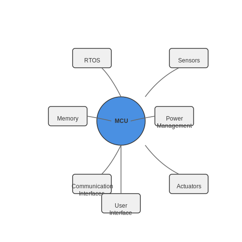
Applied SPI Protocol
1. History and Evolution of SPI
1.1 History and Evolution of SPI
The Serial Peripheral Interface (SPI) protocol has been pivotal in the advancement of high-speed data communication in embedded systems. Initially introduced by Motorola in the 1970s, SPI was conceived to support a variety of peripherals and microcontrollers while ensuring a simple and efficient means of communication through a synchronous serial interface. This section delves into the historical context of SPI, exploring its evolution and the impact it has had on electronics. The emergence of microcontrollers in the early 1980s marked a significant turning point in digital circuit communication. Before this, data transfer was primarily managed via parallel protocols, which, while effective for short distances, became cumbersome as system complexity increased. The introduction of SPI represented a paradigm shift, as it reduced the number of connections needed for communication without sacrificing speed. By offering a full-duplex communication capability, SPI enabled simultaneous data transfer in both directions, distinguishing it from simpler protocols like I2C, which traditionally allowed for only half-duplex operation. SPI's architecture consists of a master-slave relationship, where the master device controls the communication and can interact with multiple slave devices, making it particularly suitable for applications requiring rapid response times and efficient resource utilization. The early applications of SPI focused primarily on interfacing microcontrollers with memory devices and sensors. As technology progressed, the protocol found widespread adoption in a myriad of applications such as GPS modules, SD cards, and various communication interfaces for modems and sensors. Its versatility contributed to the protocol's ubiquitous nature in both consumer electronics and industrial automation. As digital systems advanced towards higher clock speeds and more complex embedded environments, developments in SPI continued. Enhancements like quad-SPI and dual-SPI emerged, allowing multiple bits to be transmitted per clock cycle. These advancements catered to the growing demand for higher data rates, reducing the communication time dramatically while maintaining the simplicity and robustness that SPI is known for. In recent years, the integration of SPI into systems on chip (SoCs) has further solidified its relevance. The seamless incorporation of SPI with advanced microcontrollers and field-programmable gate arrays (FPGAs) has allowed engineers to create sophisticated applications in real-time processing, data acquisition, and smart device design. In summary, the history of the SPI protocol reflects a continuous evolution driven by technological advancements and the ever-changing needs of electronic communication. From its inception to its current status as a crucial communication standard, SPI exemplifies how simple ideas can lead to profound impacts in the field of electronics. For further reading, please continue on to the next section, where we explore the technical specifications and operational principles of the SPI protocol.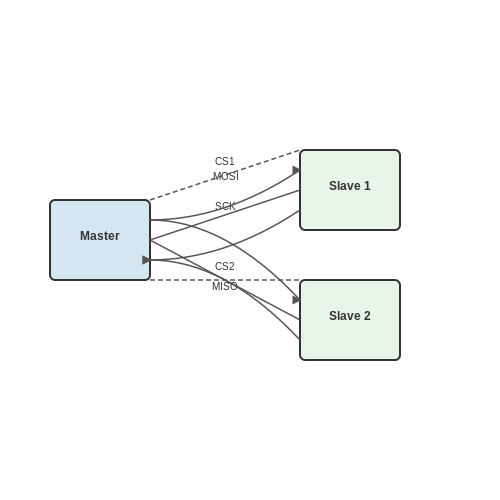
1.2 Key Features of SPI Protocol
The Serial Peripheral Interface (SPI) protocol, established by Motorola in the 1980s, is a widely adopted method for high-speed data transfer between microcontrollers and various peripherals such as sensors, memory devices, and displays. Its key features contribute to its extensive use in embedded systems and applications requiring efficient inter-device communication.
Full-Duplex Communication
One of the primary attributes of the SPI protocol is its ability to facilitate full-duplex communication, allowing simultaneous data transmission and reception. This is achieved through separate lines for data input and output, with the Master sending data while simultaneously receiving data from the Slave. The presence of two different data lines, often referred to as MISO (Master In Slave Out) and MOSI (Master Out Slave In), enhances the overall throughput of the communication process compared to half-duplex protocols, like I²C.
Configurability and Scalability
The SPI protocol supports various configurations, making it suitable for a range of applications. Notably, it allows different data word sizes (8, 16, or more bits) and clock polarities and phases, often referred to as CPOL and CPHA. This configurability is crucial, as it enables communication with a multitude of devices, each possibly adhering to different timing and data requirements. The connection of multiple Slaves is also supported via specific select lines for each peripheral, enhancing scalability in case of complex systems.
Speed and Performance
One of SPI's major advantages is its high-speed operation. SPI can achieve clock rates of several megahertz, depending on the capabilities of both the Master and Slave devices. The absence of a complex addressing mechanism allows quicker data retrieval, which is especially beneficial in applications that require fast response times, such as audio processing or real-time data acquisition in physical systems.
Simple Network Topology
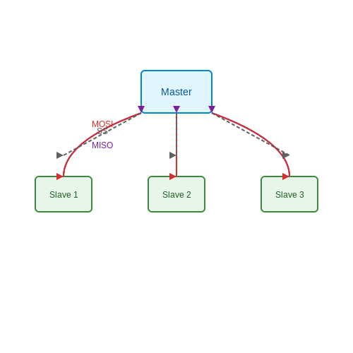
In terms of network architecture, SPI utilizes a star topology, where the Master device controls the communication. Each Slave is connected to the Master through its own Slave Select (SS) line, simplifying the interconnection and minimizing interference issues. This simplicity is advantageous in environments with multiple interconnected peripherals while maintaining efficient signal integrity.
Limitations
Despite its numerous strengths, SPI also comes with limitations. The requirement for dedicated select lines for each Slave can lead to complications in designs with multiple devices, as it increases the number of necessary I/O pins. Additionally, SPI lacks inherent error-checking mechanisms, making it crucial for designers to implement additional solutions if data integrity is a concern in critical applications.
Ultimately, the SPI protocol, with its full-duplex capabilities, configurability, high speed, and simple topology, remains a core component in the toolbox of engineers and researchers working with digital communication. Understanding its key features enhances the ability to select the appropriate protocol for specific applications, optimizing system performance and efficiency.
1.3 Applications in Modern Electronics
In the realm of modern electronics, the Serial Peripheral Interface (SPI) protocol plays a crucial role across various applications, providing a reliable and efficient means of data transfer between microcontrollers and peripheral devices. As technology continues to evolve, understanding the applications of SPI is imperative for engineers, researchers, and graduate students alike. This section delves into the diverse scenarios wherein SPI is applied, showcasing its versatility and utility.Communication with Peripheral Devices
One of the most prominent applications of SPI is in facilitating communication between a microcontroller and various peripheral devices such as sensors, memory chips, and displays. The architecture of SPI allows for full-duplex communication, meaning data can be transmitted and received simultaneously. This is achieved using distinct lines for data transmission (MOSI - Master Out Slave In, MISO - Master In Slave Out) and a dedicated clock line (SCLK), enabling efficient and rapid exchanges. A typical setup may involve a microcontroller interfacing with multiple devices. For instance:- Microcontroller: Acts as the master device controlling the communication.
- Peripheral Devices: Includes ADCs (Analog to Digital Converters), DACs (Digital to Analog Converters), and various sensors that require high-speed data transfer.
Embedded Systems and IoT Applications
Embedded systems and the rapidly growing Internet of Things (IoT) landscape greatly benefit from the SPI protocol. In many IoT devices, SPI is favored due to its simplicity in interfacing with various sensors and modules, such as temperature, humidity sensors, and display interfaces. The following points illustrate this application further:- Sensor Networks: SPI enables seamless integration of multiple environmental sensors, making it possible to monitor conditions like temperature and humidity concurrently.
- Display Technologies: SPI is widely used in displaying information on LCD and OLED screens, allowing for fast refresh rates and effective graphics rendering.
- Low Latency Needs: Many IoT applications require real-time data transmission, where SPI's high transaction speeds (up to several MHz) provide significant advantages over other protocols like I2C.
Automotive and Industrial Control Systems
In automotive applications, SPI is instrumental in controlling and interfacing with various subsystems, such as infotainment systems, engine management units, and tire pressure monitoring systems. Its robustness and fail-safety features are paramount given the safety standards in automotive designs. In industrial scenarios, SPI's ability to accommodate multiple data sources and destinations makes it suitable for applications in process automation, robotics, and machinery control. Consider the following examples:- Robotics: SPI facilitates communication between microcontrollers and sensors, enhancing the responsiveness and accuracy of robotic systems.
- Data Acquisition Systems: In high-speed data acquisition, SPI enables the simultaneous reading of multiple channels, improving system efficiency.
Extending the SPI Protocol through FPGA Integration
Field Programmable Gate Arrays (FPGAs) have recently emerged as powerful platforms for implementing SPI communication. FPGAs offer a flexible architecture that allows rapid reconfiguration of the SPI protocol to suit specific application requirements. Engineers can create custom interfaces that leverage parallel processing capabilities, thus increasing data throughput further. This customization is particularly advantageous in applications requiring modulation of clock speed and timing adjustments, ensuring seamless integration and efficient operation across devices. The combination of SPI with FPGA technology opens up new frontiers in high-performance systems, allowing greater adaptability and scalability beyond traditional microcontroller setups. Conclusion The applications of the SPI protocol across various domains highlight its essential role in contemporary electronic designs. Its high-speed operation, low complexity, and ability to support multiple slave devices make it an indispensable tool in the toolbox of engineers and researchers alike. As technology advances, continued exploration of SPI applications will likely yield even more innovative uses, particularly within the realms of high-speed data communication and embedded systems solutions.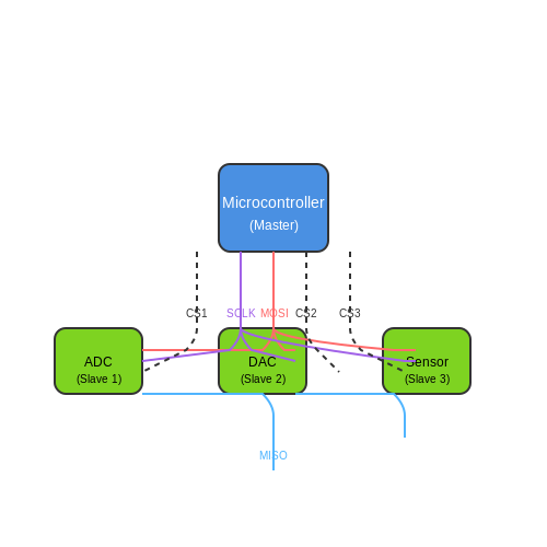
2. SPI Architecture and Components
2.1 SPI Architecture and Components
The Serial Peripheral Interface (SPI) protocol is a synchronous, full-duplex communication interface designed for short-distance communication primarily between microcontrollers and peripheral devices. Understanding its architecture and components is crucial for effectively implementing SPI in various applications, particularly as embedded systems and IoT devices proliferate.
At its core, the SPI architecture involves a master-slave configuration, which can include multiple slaves attached to a single master. This architecture allows straightforward data transfer and system design where the master device initiates the communication.
Key Components of SPI
The fundamental components of SPI include:
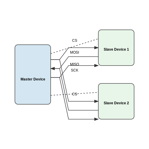
- Master Device: The device that controls the communication, generates the clock signal, and initiates data transfers.
- Slave Device: One or more devices that respond to the master's commands. They listen for clock signals and data sent from the master.
- Serial Clock (SCK): A clock signal generated by the master to synchronize data transfer. The frequency of this clock can affect data transfer rates and system performance.
- Master Out Slave In (MOSI): Line used for data communication from the master to the slave. The data is serially transferred to the slave device.
- Slave Out Master In (MISO): Line used for data communication from the slave back to the master, providing feedback or sensor readings.
- Chip Select (CS): Also known as Slave Select (SS), this line is used by the master to select the appropriate slave device for communication. Each slave requires a dedicated CS line that the master can enable or disable.
Understanding Data Flow
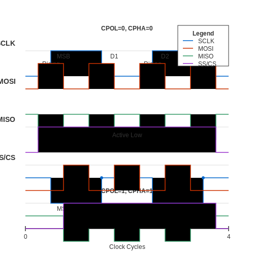
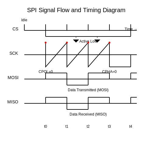
When initiating communication, the master activates the appropriate CS line corresponding to the desired slave. Following this, the master generates the SCK signal, allowing data to be sent through the MOSI line. The slave, while listening to this clock pulse, reads the incoming data bit, responding as necessary through the MISO line.
The synchronous nature of SPI allows for data to be transmitted simultaneously while a clock signal regulates the timing, making it efficient for high-speed applications. This efficiency is a major reason SPI is prevalent in applications like sensors, memory devices, and real-time data acquisition systems.
Applications and Practical Relevance
Once you have a firm grasp of the architecture and components of SPI, you can explore its applications. SPI is extensively used in:
- Microcontrollers: Providing communication between the microcontroller and external memory or peripherals, such as ADCs/DACs (Analog-to-Digital Converters/Digital-to-Analog Converters).
- Wireless Modules: Facilitating communication for wireless sensors and actuators in remote monitoring applications.
- Display Interfaces: Enabling communication with LCDs and OLEDs for graphical displays.
This flexibility, combined with its capability for high data throughput, makes SPI a vital protocol in modern electronics design. Advanced systems often implement SPI due to its balance of simplicity and efficiency, particularly as more devices require real-time data sharing.
2.2 SPI Communication Process
The Serial Peripheral Interface (SPI) communication process is essential for enabling fast and efficient data transfer between microcontrollers and peripheral devices. At its core, SPI is a synchronous serial communication protocol that primarily utilizes four key signals to facilitate data transfer: Master Out Slave In (MOSI), Master In Slave Out (MISO), Serial Clock (SCK), and Slave Select (SS). Understanding how these signals interact provides clarity on the intricacies of SPI communications, paving the way for practical applications in diverse electronic systems. The initiation of an SPI communication session typically begins with the Master device asserting the Slave Select (SS) line low, indicating that communication will commence with the selected Slave device. In this context, it is important to note that multiple Slave devices can be connected to a single SPI bus, distinguished by their unique Slave Select lines. Once the Slave device recognizes the active SS line, data transmission begins with the Master device generating clock pulses on the Serial Clock (SCK) line. Each clock pulse denotes the timing for data transmission; specifically, it synchronizes the data flow on the MOSI and MISO lines. The data is shifted out from the Master through the MOSI line while simultaneously being shifted in through the MISO line. The format of the data sent over these lines is typically a defined number of bits, commonly 8 bits for many applications. It's important to understand that SPI allows for full-duplex communication, meaning that data can be sent and received simultaneously. This is one of the key advantages over other protocols such as I2C, making SPI favorable in applications requiring robust and high-speed data transactions. The ability to transmit data concurrently empowers SPI to achieve higher throughput, particularly beneficial in scenarios involving high-speed sensors or display interfaces. The timing of data bits is generally characterized by two key parameters: clock polarity (CPOL) and clock phase (CPHA). The selection of these parameters determines the precise moment the data is sampled and shifted. When these settings are misconfigured between the Master and Slave devices, it can lead to corrupted data or communication failure. In practice, once the data transmission is complete, the Master device releases the SS line, signaling the end of communication. This allows the Slave device to process the retrieved data and potentially send a response during subsequent communications. One real-world application of SPI is in interfacing microcontrollers with flash memory chips, where its high-speed data transfer capabilities allow rapid programming and retrieval of data. Another application includes connecting sensors such as accelerometers or gyroscopes that may require constant polling and rapid data transfer.- Clock Generation: Establishing the clock speed is crucial, as it dictates the maximum operational speed of the SPI communication. Base speeds commonly range from a few kHz up to several MHz, depending on the devices in use.
- Data Framing: Data framing refers to how bits are organized before transmission. Typically, devices may transmit data as bytes, offering versatile framing options depending on the application requirements.
- CS Handling: The management of the Chip Select (CS) line should be consistent to avoid bus contention, especially when multiple devices are present on the SPI bus.
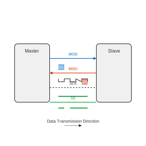
2.3 Data Transmission Format
The Serial Peripheral Interface (SPI) protocol is quintessential in the realm of high-speed synchronous data transfer, particularly in microcontroller and peripheral communications. Grasping the data transmission format of the SPI is essential for demonstrating how data is efficiently transmitted and interpreted between devices.Overview of SPI Data Transmission
At its core, SPI operates on a master-slave architecture, facilitating communication between a master device and one or more slaves. The data transmission occurs on dedicated lines: a clock line (SCK), a master output slave input line (MOSI), a master input slave output line (MISO), and a slave select line (SS). During an SPI transaction, the master device generates the clock signal to synchronize the data exchange. The master transmits data on the MOSI line, while the slave device responds through the MISO line, both in sync with the clock signals.Format of Data Transmission
The structure of transmitted data in SPI comprises the following elements:- Data bits: SPI allows transmission of data in various bit sizes, typically 8, 16, or 32 bits, depending on the application. This flexibility enables efficient communication tailored to the needs of specific peripherals.
- Direction of Transmission: The direction in which data is sent can either be from the master to the slave (MOSI) or from the slave to the master (MISO). The simultaneous bidirectional nature of SPI enhances its performance, making it advantageous over other serial protocols.
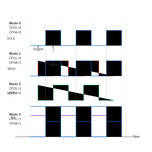
- Clock Polarity (CPOL) and Clock Phase (CPHA): The timing characteristics of the clock influence the data sampling. CPOL defines the idle state of the clock, while CPHA determines when data is latched. The configuration can lead to four different mode combinations, denoted as Mode 0 through Mode 3.
Data Packet Structure
When we consider the data packet for transmission, it often comprises several components: 1. Start Bit(s): Used to signal the beginning of a data frame; may not always be explicitly defined in SPI but is implicit in the clock's behavior. 2. Data Field: This encompasses the actual data bits being transmitted. For instance, transmitting a value of `10110011` as an 8-bit data frame will occur bit by bit in synchronization with the clock. 3. End Bit(s): While traditional UART communication utilizes stop bits, SPI uses the cessation of clock pulses to indicate the end of data transmission. To visualize the overall transmission format, one can depict a timing diagram that illustrates the clock signal in relation to the MOSI and MISO data lines. This timing diagram can encapsulate the interaction well, showing how data transitions occur per the clock cycles.Practical Implications and Applications
The understanding of data transmission format within SPI is not merely academic but underpins practical applications such as: - Embedded Systems: SPI is prevalent in microcontroller communication with sensors, displays, and memory devices, ensuring low-latency transactions in real-time systems. - Automotive Applications: SPI's efficiency is harnessed in automotive sensor data exchange, aiding in processes such as engine monitoring and control systems. - Signal Processing: In instrumentation, SPI is commonly used for fast data acquisition systems due to its high-speed transfer capabilities. In conclusion, comprehending the data transmission format in SPI is fundamental for engineers and researchers aiming to design robust systems capable of efficient interfacing among diverse electronic components. By mastering how data is structured and transmitted, one can harness the full potential of the SPI protocol in advanced technological applications.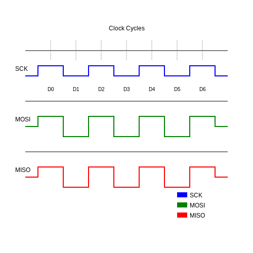
3. Clock Polarity and Phase
3.1 Clock Polarity and Phase
The Serial Peripheral Interface (SPI) protocol is widely used in embedded systems for communication between microcontrollers and peripheral devices. A fundamental aspect of SPI communication is the clock signal that synchronizes data transmission. Two critical parameters of the clock signal are Clock Polarity (CPOL) and Clock Phase (CPHA), which dictate how data is exchanged on the SPI bus.
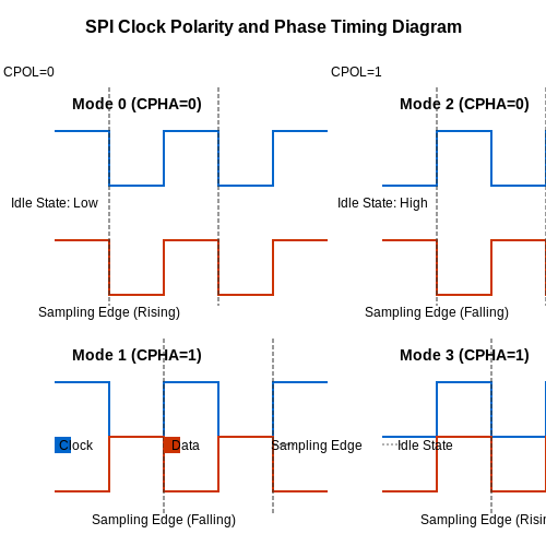
Clock Polarity defines the idle state of the clock signal. Specifically, it can either be high or low when the line is idle. When the clock is idle high (CPOL = 1), data is sampled on the rising edge of the clock signal, whereas if the clock idles low (CPOL = 0), data is sampled on the falling edge. This subtle difference provides flexibility in communication, accommodating various peripheral devices that may expect a specific clock state during idle.
Clock Phase and Its Importance
Clock Phase refers to the timing relationship between the clock edge and the data signal. This parameter determines when data is sampled (read) and when it is valid. The two configurations are:
- CPHA = 0: Data is sampled on the first clock edge (when going from idle to active). The data on the bus must be stable before the clock transitions.
- CPHA = 1: Data is sampled on the second clock edge (when the clock transitions from active back to idle). Here, the data becomes valid after the first clock edge.
The combination of CPOL and CPHA creates four different modes, categorically known as SPI Modes 0 through 3. Structuring the signal like this allows SPI to maintain compatibility with various hardware implementations:
- Mode 0: CPOL = 0, CPHA = 0
- Mode 1: CPOL = 0, CPHA = 1
- Mode 2: CPOL = 1, CPHA = 0
- Mode 3: CPOL = 1, CPHA = 1
Choosing the correct settings for CPOL and CPHA is crucial as it directly affects communication reliability. For instance, if an SPI master uses Mode 0 while the slave device operates in Mode 1, data may become corrupted due to the misalignment of clock edges, illustrating the importance of matching these parameters.
Real-World Applications
In practice, understanding and configuring clock polarity and phase is pivotal in various fields, including:
- Embedded Systems: Microcontroller-to-sensor communication often relies on SPI, necessitating compatible settings for reliable data exchange.
- Microprocessor Interfaces: Many graphics controllers and memory chips utilize SPI protocols, where mismatched clock configuration can lead to severe operational issues.
- Industrial Automation: Efficient data transfer between devices, such as ADCs and DACs, within industrial environments requires precise timing parameters.
Thus, an engineer or designer must carefully evaluate device specifications to ensure correct settings for SPI communication. As technologies evolve and more devices leverage this protocol, a strong grasp of clock polarity and phase will remain a fundamental skill for professionals in electronics and embedded systems.
3.2 Setup and Hold Timing Requirements
In the context of the Serial Peripheral Interface (SPI) protocol, understanding the setup and hold timing requirements is critical for establishing reliable communication between the master and slave devices. These parameters ensure that data is correctly interpreted during data transmission, which directly affects the integrity and performance of the communication system.
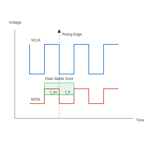
The setup time is the duration that data signals must remain stable prior to the relevant clock edge. Conversely, the hold time refers to the duration that the data signals must remain stable after the clock edge has occurred. Both parameters are essential for synchronizing the master and slave devices and guaranteeing that the transmitted data can be accurately captured.
Setup Timing Requirements
The setup time, usually denoted as tsu, specifies how long the data signals must stabilize before the rising edge of the clock signal. Failure to meet this timing requirement can lead to incorrect sampling of the data by the slave device. Mathematically, it can be expressed as:
Where tmin is the minimum setup time specified in the device's data sheet. In practical terms, if the tsu is not adhered to, bit errors may occur, resulting in data corruption. This can significantly impact applications in fields such as telecommunications, medical devices, and industrial automation, where precise data integrity is crucial.
Hold Timing Requirements
The hold time, denoted as th, defines the minimum duration that the data signals must remain stable after the clock edge. Similarly, this parameter is critical as it ensures that the slave device has sufficient time to latch and accurately process the incoming data. This timing can also be expressed mathematically:
Where tmin represents the minimum hold time in the specification. Not respecting the hold time can also lead to erroneous data capture, which is particularly detrimental in high-speed applications where timing margins are tight.
Historical Context and Practical Implications
The need for stringent setup and hold timing requirements can be traced back to the original development of synchronous communication protocols. As systems have evolved, the importance of reliability in data transmission has expanded, prompting the development of advanced timing analysis techniques and simulation tools. In modern microcontrollers and digital communication systems, emerging technologies emphasize optimizing both timing parameters to enhance overall system performance.
In practice, engineers must account for the propagation delays introduced by interconnecting circuits, as well as clock skew when designing SPI communication systems. This is particularly relevant for high-speed applications where delays can hinder overall throughput and reliability.
Tools such as timing analyzers and simulators can be employed to visualize and analyze the timing characteristics in SPI setups. This not only ensures compliance with the specified requirements but also facilitates optimization in system design.
For engineers and researchers, understanding and applying these concepts correctly can lead to enhanced system performance, reduced errors, and reliable device interactions in myriad applications.
3.3 Voltage Levels and Logic States
In the context of the Serial Peripheral Interface (SPI) protocol, understanding voltage levels and logic states is crucial for effective communication between microcontrollers and peripheral devices. SPI operates using a straightforward but essential principle: the transmission of digital information that is represented by two distinct voltage levels corresponding to binary logic states—typically referred to as logic "high" and logic "low." The selection of voltage levels in SPI communications is primarily dictated by the supply voltage (Vcc) of the devices involved. For example, in a typical 3.3V system, a logic high might be defined as voltages that are 0.7 times Vcc (approximately 2.3V in this case) or greater, while a voltage close to 0V will represent a logic low. Conversely, in a 5V system, these thresholds would be proportionally higher as well.Understanding Logic Levels
When different systems with varying voltage levels interface, it is critical to prevent miscommunication. For instance, if a 3.3V microcontroller attempts to communicate with a 5V peripheral, improper voltage could result in data corruption or even damage to the components. In practice, this issue is addressed through the use of level shifters or voltage dividers, which adapt the voltage levels between the two devices, ensuring compatibility. The critical logic states can be summarized as follows:- Logic Low (0): Typically between 0V and about 0.3V of Vcc.
- Logic High (1): Usually from about 0.7V of Vcc to Vcc.
- 3.3V TTL: Logic Low: 0V to 1.0V; Logic High: 2V to 3.3V.
- 5V TTL: Logic Low: 0V to 1.5V; Logic High: 3.5V to 5V.
Real-World Applications
Understanding these voltage levels is not an abstract concept but rather a pivotal factor in circuit design and integration. For instance, when designing devices such as sensors, displays, or communication modules, engineers must specify compatible voltage ranges to ensure robust performance. Failure to do so can lead to significant issues in electronic communication, including signal distortion, unexpected resets, or component damage. Implementing level shifting mechanisms is a practical solution for interfacing devices that operate at differing voltage levels. In many cases, dedicated ICs or simple resistor-based level shifting circuits facilitate these connections, thus maintaining the integrity of the communication. In summary, the careful consideration of voltage levels and logic states in SPI communications plays a fundamental role in ensuring compatibility and reliability across diverse electronic systems. As systems continually evolve, engineers must remain vigilant in observing the specifications to preemptively address potential interfacing issues. This foundational understanding will undoubtedly empower engineers and researchers as they innovate and integrate various electronic components in advanced applications.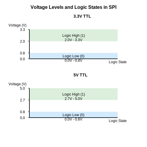
4. Setting Up SPI in Microcontrollers
4.1 Setting Up SPI in Microcontrollers
The Serial Peripheral Interface (SPI) protocol allows for efficient data transfer between microcontrollers and peripheral devices. Understanding its setup is crucial for engineers and researchers aiming to leverage SPI's capabilities in projects ranging from simple sensor readings to complex device communications. This section provides a comprehensive guide on establishing SPI in microcontrollers, focusing particularly on initialization, configuration, and real-world applications.
Understanding SPI Configuration
Before diving into specific microcontroller implementations, it's important to grasp essential parameters that define SPI behavior:
- Clock Polarity (CPOL): Defines the idle state of the clock; if the clock is high when idle, the CPOL is set to 1, and if low, it is set to 0.
- Clock Phase (CPHA): Specifies whether data is sampled on the leading or trailing edge of the clock pulse. A CPHA value of 0 means data is sampled on the first clock edge.
- Bit Order: Determines the order in which bits are transmitted, either Most Significant Bit First (MSB) or Least Significant Bit First (LSB).
- Data Rate: This sets the frequency of the clock signal, which needs to be considered against the speed of the peripheral's capabilities.
Initial Setup Process
The process of setting up SPI in a microcontroller involves several steps, typically starting with enabling the SPI module and configuring pins. The following is a structured approach:
1. Enable the SPI Module
Most microcontrollers provide specific registers that need to be set to activate the SPI peripheral. For instance, in an Atmel-based microcontroller, you would configure the SPI control register.
2. Configure GPIO Pins
Designate the appropriate pins for SPI communication. This includes:
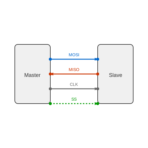
- MOSI (Master Out Slave In): Transmits data from the master to the slave.
- MISO (Master In Slave Out): Transfers data from the slave to the master.
- CLK (Clock): Carries the clock signal generated by the master.
- SS (Slave Select): Used by the master to select the active slave device.
3. Set the SPI Parameters
Next, configure the parameters (CPOL, CPHA, bit order, and data rate) in the relevant control registers. For example:
This hypothetical equation expresses how the control register (SPCR) can be set by combining configuration bits for SPI operation. Actual register names and operations may vary based on the specific microcontroller architecture.
4. Initiate Communication
With the SPI module configured, the master can initiate communication with the slave by pulling the SS line low, sending the required data over the MOSI pin while synchronizing the clock over the CLK line. The code snippet below gives a conceptual example of a typical transaction.
#include

void SPI_init() {
    // Set MOSI and SCK as Output
    DDRB = (1<
This code initializes the SPI interface on an AVR microcontroller and includes a function to transmit data over SPI. Developers should adjust the code to fit their chosen microcontroller's API and environment.
Real-World Application Examples
The SPI protocol finds applications in a range of devices, such as:
- Memory Devices: Reading from Flash and EEPROM memory chips.
- Sensor Data Acquisition: Collecting data from various sensors including temperature sensors and accelerometers.
- Display Interfaces: Driving OLED or LCD displays for embedded systems.
Understanding how to efficiently set up SPI in microcontrollers can significantly enhance the robustness and efficiency of your electronic projects. As applications for fast serial communication continue to expand, mastering SPI remains an indispensable skill in the toolkit of an advanced engineer or researcher.
4.2 Sample Code for SPI Communication
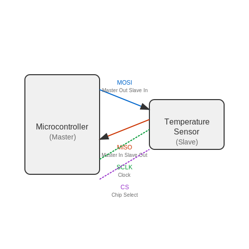
The Serial Peripheral Interface (SPI) protocol is a pivotal element in communication between microcontrollers and peripheral devices. As an advanced concept, understanding and implementing SPI requires both theoretical insight and practical coding abilities. This section provides sample code demonstrating SPI communication, utilizing a typical microcontroller setup. Here, we explore a scenario where a microcontroller communicates with a temperature sensor using SPI, facilitating real-time data acquisition and control.
SPI Communication Overview
Before diving into the code, it's essential to grasp the mechanics of SPI. SPI communicates over four lines: Master Out Slave In (MOSI), Master In Slave Out (MISO), Clock (SCLK), and Chip Select (CS). The master device (in this case, the microcontroller) controls the clock and initiates data transmission, while the slave (the temperature sensor) responds with the requested information.
Sample Code Implementation
Below is a sample code demonstrating SPI communication with a temperature sensor. The code is written for a microcontroller, showcasing C programming syntax commonly used in embedded systems development. This example presupposes that the reader has already set up the necessary hardware connections and libraries.
#include

const int CS_PIN = 10;  // Chip Select pin

void setup() {
    Serial.begin(9600);
    SPI.begin(); // Initialize SPI
    pinMode(CS_PIN, OUTPUT);
    digitalWrite(CS_PIN, HIGH); // Set CS high to start
}

void loop() {
    digitalWrite(CS_PIN, LOW); // Activate the sensor
    byte data = SPI.transfer(0b00000000); // Send dummy byte to receive data
    digitalWrite(CS_PIN, HIGH); // Deactivate the sensor

    // Assuming data represents the temperature
    Serial.print("Temperature Reading: ");
    Serial.println(data);

    delay(1000); // Delay before the next reading
}
In this code snippet:
- The setup() function sets up the serial communication and initializes SPI.
- The loop() function continuously reads data from the temperature sensor every second.
- The SPI.transfer() function sends a dummy byte to initiate the clock, allowing the sensor to send back the temperature data.
This basic implementation offers a foundational model for SPI communication. You can expand this code to include more complex interactions, such as handling multiple slaves or more intricate data formatting from the sensor.
Practical Applications
SPI protocol's high-speed capabilities make it suitable for various applications beyond temperature sensing, including:
- Data acquisition systems for monitoring environmental conditions.
- High-speed ADCs in audio processing applications.
- Image sensors in camera systems for rapid image processing.
As technology advances, the versatility of SPI in connecting multiple peripherals efficiently continues to prove its relevance in modern embedded systems.
4.3 Debugging SPI Connections
Debugging SPI (Serial Peripheral Interface) connections presents unique challenges due to the rapid data transmission and specifics of timing requirements involved in its operation. Understanding effective debugging techniques is essential for engineers and researchers, particularly when working with high-speed applications such as sensor interfacing or communication between microcontrollers.
Identifying Common Issues
Before diving into specific tools and techniques, it's important to recognize typical issues that can arise with SPI connections:
- Clock Signal Integrity: The SPI clock must be clean and stable. Any noise or distortion can cause miscommunication between devices.
- Signal Level Mismatches: Devices connected via SPI may not be compatible due to differing voltage levels. Ensure that signal levels are appropriately matched, employing level shifters when necessary.
- Data Frame Mismatches: Confirm that both the master and slave devices adhere to the same data frame formats (e.g., bit order, data length).
- Incorrect Chip Select Management: Mismanagement of the chip select (CS) line can lead to improper communication. Ensure the CS pin is activated before data transmission and deactivated afterward.
- Timing Violations: Closely observe the timing requirements for setup and hold times, as outlined in the device specifications.
Tools for Debugging SPI
Several methods and tools are available for effective debugging of SPI connections. The following are particularly useful:
Logic Analyzers
Logic analyzers are invaluable for capturing and analyzing digital signals in your SPI setup. They allow you to visualize waveforms and timing diagrams, making it easier to identify issues such as incorrect signal timing or data corruption. Typically, the process involves:
- Connecting the logic analyzer's probes to the SCK (clock), MOSI (master out slave in), MISO (master in slave out), and CS (chip select) lines.
- Configuring the logic analyzer to capture SPI protocol data by setting appropriate sample rates and SPI settings.
- Interpreting the captured data to verify whether the signals adhere to expected patterns based on the specific protocol implementation.
Oscilloscopes
Oscilloscopes can complement logic analyzers by providing a time-resolved view of individual signals. They allow for direct viewing of the voltage levels over time for the SPI signals, which can be helpful in diagnosing problems such as signal integrity issues. Key steps include:
- Configuring the oscilloscope to trigger on the clock edge to ensure relevant data is captured during SPI transmission.
- Examining the timings between clock and data lines to look for setup and hold time violations.
Software Debugging
On the software side, implementing comprehensive logging to track the state of SPI communications can help pinpoint issues. Some strategies include:
- Check Return Values: Ensure that your software checks return values from SPI read and write functions to detect failures in data transmission.
- Debug Outputs: Print debug outputs to serial or console during SPI transactions to observe the flow of control and data.
- Error Handling: Implement robust error handling to manage unexpected states and recover gracefully from failures.
Conclusion
Debugging SPI connections requires a thoughtful combination of hardware tools and software techniques. By systematically addressing common issues with appropriate tools—such as logic analyzers and oscilloscopes—engineers can significantly enhance the reliability and performance of SPI communication systems. As devices become more interconnected and data transfer rates continue to climb, mastering these debugging skills will be essential for advanced practitioners in fields such as embedded systems, robotics, and industrial automation.
5. Multi-Slave Configuration
5.1 Multi-Slave Configuration
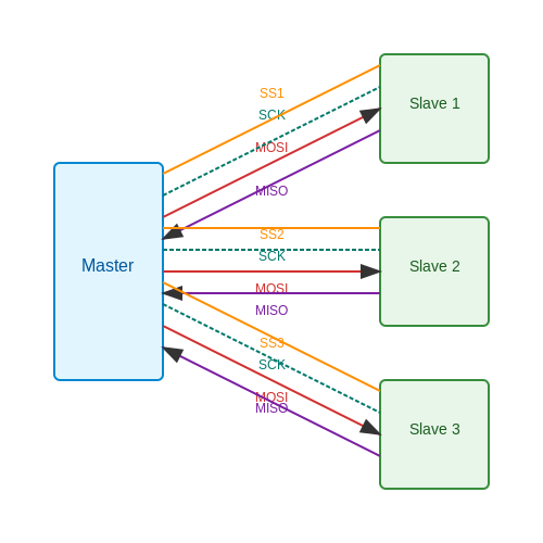
The Serial Peripheral Interface (SPI) protocol is highly valued for its simplicity and versatility in establishing communication between microcontrollers and peripheral devices. As applications become more complex, a multi-slave configuration becomes essential. This configuration allows multiple slave devices to connect to a single master, facilitating efficient communication without the need for multiple dedicated master devices.
In a typical SPI architecture, the master initiates communication and controls the clock signal, while the slaves respond to the master's commands. When multiple slave devices are involved, specific considerations must be addressed to ensure seamless operations.
Signal Lines and Wiring Considerations
In a multi-slave SPI configuration, the system utilizes four primary signal lines:
- MOSI (Master Out Slave In): The line for sending data from the master to the slaves.
- MISO (Master In Slave Out): The line for sending data from the slaves back to the master.
- SCK (Serial Clock): The clock signal generated by the master for synchronization.
- SS (Slave Select): A separate slave select line is needed for each slave device to activate the desired slave for communication.
Each slave is connected via its dedicated SS line, which the master can control to specify which slave device is currently active. The master pulls the appropriate SS line low to enable the corresponding slave device and must ensure that all other SS lines are kept high to prevent unwanted interference.
Addressing and Communication Protocol
In this configuration, addressing is a critical aspect. The master must maintain an accurate control mechanism, often incorporating an address or command byte in the initial transmission to notify the active slave of upcoming data. The following steps can help streamline communication:
- Initialization: The master initializes communication and sets the desired clock polarity and phase.
- Select Slave: The master pulls the SS line of the target slave low.
- Data Transfer: Engage in SPI transactions (sending and receiving data).
- Deselect Slave: After communication, the master pulls the SS line high to deactivate the slave.
Performance Considerations
While a multi-slave configuration provides flexibility, it can introduce delays. As multiple slaves share the same signals, the increased capacitance on the lines can affect the maximum achievable clock rate. Therefore, it’s essential to consider factors such as cable length and the electrical characteristics of the circuits when designing the communication system.
Real-World Application
Multi-slave SPI configurations are widely adopted in consumer electronics, automotive systems, and embedded applications, where multiple sensors, displays, or memory devices are interfaced to a microcontroller. For example, a microcontroller in a drone may use SPI to gather data simultaneously from multiple sensors such as an accelerometer, gyroscope, and magnetometer, optimizing performance while keeping the footprint compact.
Conclusion
Implementing a multi-slave configuration in SPI can significantly enhance system capabilities and reduce the complexity of device management. Understanding the functional principles and challenges of this setup is crucial for engineers aiming to develop efficient and robust communication solutions in advanced electronic systems.
5.2 SPI Performance Optimization Techniques
To enhance the performance of a Serial Peripheral Interface (SPI) communication, engineers can employ a variety of optimization techniques that not only increase the transmission speed but also improve the overall reliability of the system. Understanding these techniques is critical for advanced applications where timing and data integrity are paramount.Clock Rate Optimization
One of the most straightforward methods to optimize SPI performance is by maximizing the clock rate. The SPI clock, generated by the master device, dictates the speed at which data is transferred between the master and slave devices. The permissible clock frequency depends on the specifications of the devices involved. In practice, to determine the optimal clock frequency, consider the following equation derived from Nyquist's sampling theorem:Minimize Overhead
Reducing protocol overhead can lead to significant performance enhancements. This involves optimizing the number of bits transferred in each operation and minimizing the number of commands required to complete a task. In SPI, a trade-off often exists between frame size and the number of transactions: - Daisy Chaining: If multiple slaves are present, consider daisy chaining the devices to reduce the number of select lines and transactions. - Burst Mode Transmission: Some SPI slaves support burst mode, allowing multiple data bytes to be sent in a single transaction, thus reducing the protocol overhead associated with transfer initiation.Data Formatting
Ensuring that data is formatted correctly for the specific application can also aid in optimization. For instance, using the appropriate data structure can minimize the amount of data sent or received. Data compression techniques might also be applicable in scenarios requiring the transfer of bulk data.Hardware Considerations
Beyond protocol optimization, hardware limitations can affect SPI performance. Utilizing faster microcontroller architectures with superior processing power and optimized GPIO driving capabilities can significantly decrease communication delays. Careful consideration of the following factors can yield improvements: - Signal Integrity: Ensuring proper termination and utilizing components rated for the desired frequency can minimize issues such as reflections and signal dropouts. - Layout Design: PCB layout plays a vital role in maintaining signal integrity. Short, direct traces with proper grounding are essential for high-frequency signals.Implementing FIFO Buffers
For systems with high data throughput requirements, implementing First In First Out (FIFO) buffers can significantly enhance SPI communication. A FIFO buffer temporarily holds data as it is being read or written, allowing the processor to continue its operations without waiting for the transmission to complete. This is especially useful in applications involving high data rates where latency can hinder performance.Testing and Validation
Finally, the effectiveness of any optimization technique should be validated through rigorous testing. Utilizing tools such as logic analyzers or SPI protocol analyzers can provide insights into data integrity, timing, and overall system performance. Through systematic profiling of SPI transactions, engineers can identify bottlenecks and establish a more responsive and reliable system tailored to their specific application needs. By integrating these performance optimization techniques, engineers can realize significant enhancements in SPI communication, thereby extending the potential of their electronic systems in real-world applications, such as in robotics, automotive systems, and high-speed data acquisition.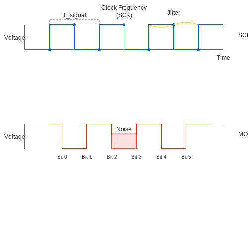
5.3 Error Handling in SPI Communication
The Serial Peripheral Interface (SPI) protocol is renowned for its simplicity and high-speed communication capabilities, but, like any communication protocol, it is not immune to errors. Error handling in SPI is vital to ensure data integrity and efficient system operation. This section delves into the types of potential errors, approaches for error detection, and correction mechanisms designed to maintain robust communication in SPI systems.
Understanding Types of Errors in SPI Communication
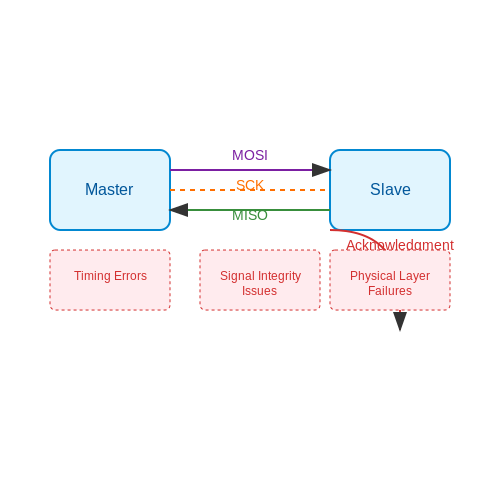
In SPI communication, various errors may occur primarily due to timing mismatches, fault conditions, signal integrity issues, and device malfunctions. These errors can be categorized into:
- Timing Errors: These arise from incorrect clock speeds or phase misalignment between the master and slave devices. Each device must adhere strictly to the defined timing parameters to avoid data corruption.
- Signal Integrity Issues: Electrical noise, crosstalk, or reflections can distort the signals, causing erroneous readings or data loss. Proper hardware layout and termination become critical in mitigating these issues.
- Physical Layer Failures: Issues such as broken connections, short circuits, or component failures can prevent successful communication. Real-world systems must include mechanisms to detect these failures quickly.
Error Detection Techniques
Before dealing with errors, it is essential to identify them. SPI itself does not include dedicated error detection capabilities; however, engineers can implement several strategies:
- Checksum or CRC: Adding a checksum or Cyclic Redundancy Check (CRC) can verify the integrity of transmitted data. By calculating these values prior to transmission and verifying them at the receiving end, devices can detect inconsistencies. For instance, if the transmitted data and computed CRC do not match on the receiving side, an error is flagged.
- Acknowledgment Signals: Implementing an acknowledgment (ACK) mechanism can improve error detection. The receiver confirms receipt of a correct message by sending back an ACK signal. If the sender does not receive this ACK within a specified time, it can infer that an error has occurred, prompting a resend.
Error Correction Mechanisms
Once an error is detected, correcting it is the next critical step. There are various methods available:
- Data Resend Mechanism: This straightforward approach involves the master device detecting a failure (e.g., through a timeout on the ACK signal) and requesting the enqueued data to be retransmitted. This can be an effective solution in environments where data integrity is paramount.
- Multiple Reads and Majority Voting: To address transient errors, devices can perform multiple reads of the incoming data. If variations occur, the most frequently received value can be taken as the correct data. This method, while reliable, does incur a time penalty and increased bandwidth usage.
- Using Redundant Channels: Creating redundancy by employing multiple SPI channels for the same data transmission can also aid in correcting errors. This is more resource-intensive but highly reliable for critical applications that demand fail-safe mechanisms.
Practical Implications and Real-World Applications
Implementing robust error handling in SPI communication has immediate benefits for various applications, from embedded systems in consumer electronics to industrial automation controls. In consumer devices, such as smartphones and smart home gadgets, reliable communication between components ensures functionality and user satisfaction. In industrial scenarios, such as robotic systems, ensuring the precision of command signals can be critical to operational safety.
Utilizing error handling techniques not only enhances performance but also contributes to system resilience, allowing engineers to deploy SPI communication confidently in demanding environments. Additionally, as systems grow more complex, incorporating these methods becomes vital to safeguard against expanded data flow and inter-device communication.
Conclusion
Effective error handling in SPI communication technologies is essential for preserving data integrity and enhancing communication reliability. By understanding potential error types, employing appropriate error detection strategies, and integrating correction mechanisms, engineers can ensure seamless operation, thereby realizing the full potential of SPI in their designs.
6. Using SPI with Sensors
6.1 Using SPI with Sensors
The Serial Peripheral Interface (SPI) protocol is widely adopted in electronics, especially for communication with sensors. This section delves into utilizing SPI to interface with various sensors, illuminating both the underlying principles and practical applications.Understanding SPI in the Context of Sensors
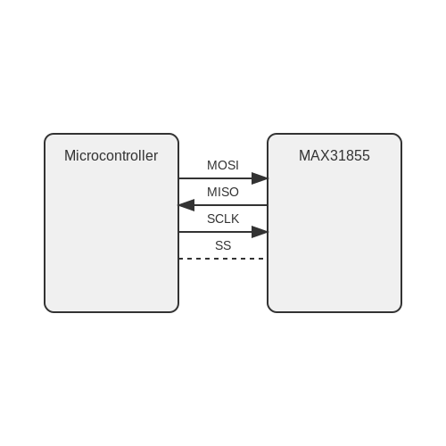
The SPI protocol enables high-speed communication between a master device and multiple slave devices, making it particularly suitable for sensor applications where rapid data acquisition is necessary. Typically, an SPI interface is characterized by four essential lines: *MISO* (Master In Slave Out), *MOSI* (Master Out Slave In), *SCLK* (Serial Clock), and *SS* (Slave Select). The master generates the clock signal and initiates data transfers while slaves respond according to the selected device.Benefits of Using SPI with Sensors
The advantages of employing SPI for sensor communication include:- High Speed: SPI can operate at clock speeds frequently exceeding 10 MHz, enabling fast data transfer, essential for real-time applications.
- Full-Duplex Communication: This allows simultaneous transmission and reception of data, which is beneficial when both CS and data need to be communicated at once.
- Simplicity: The protocol does not require complex handshaking, resulting in straightforward implementation.
- Multiple Device Support: The configuration allows multiple slaves with individual selections, enhancing system flexibility.
Common Sensor Types Interfaced via SPI
A variety of sensors utilize the SPI protocol, each designed to fulfill specific roles. Below are a few notable examples:- Temperature Sensors: Devices like the MAX31855 provide temperature readings by converting thermocouple inputs into digital data using SPI communication.
- Pressure Sensors: Sensors such as the Bosch BMP280 output pressure readings via SPI, allowing for accurate atmospheric pressure measurement in environmental monitoring.
- Accelerometers: The ADXL345, a low-power 3-axis accelerometer, employs SPI to relay motion and orientation data to a microcontroller effectively.
Basic Implementation Steps
To successfully interface a sensor via SPI, one needs to follow a systematic approach: 1. Pin Configuration: Identify and connect the SPI lines—MOSI, MISO, SCLK, and SS—between the master device (e.g., microcontroller) and the sensor. 2. Initialization: Configure the SPI settings on the master, such as clock polarity, phase, and speed, ensuring compatibility with the sensor’s specifications. 3. Data Acquisition: Implement routines to send and receive data. Typically, this involves sending a command to select the desired operation mode (e.g., read temperature) and subsequently reading the response. 4. Processing the Data: Convert the received data into meaningful values using the sensor’s datasheet to interpret the signals accurately.Example: Interfacing an SPI Temperature Sensor
Suppose you want to interface the MAX31855 temperature sensor. The setup would require configuring your microcontroller's SPI interface with the appropriate parameters specified in the MAX31855 datasheet.Relevant Data Format
The MAX31855 outputs a 32-bit value where the first 16 bits represent the temperature in degrees Celsius, with the sign bit determining negative values. To convert this into usable temperature data, one must first read the 32 bits and then extract and convert the relevant bits. Here’s a basic outline of how you would implement this in code:// Initialize SPI
SPI.begin();
digitalWrite(SS, LOW); // Select the sensor
uint32_t data = SPI.transfer32(0x00); // Read data
digitalWrite(SS, HIGH); // Deselect the sensor
// Extract temperature
int temperature = (data >> 18) & 0x3FFF; // Calculate temperature
if (data & (1 << 19)) temperature = -temperature; // Check for negative values
temperature *= 0.25; // Convert to Celsius
Challenges and Considerations
While utilizing SPI with sensors can be highly efficient, certain challenges may arise:- Signal Integrity: At higher speeds, signal degradation becomes an issue, necessitating short traces and appropriate grounding to ensure clarity.
- Multiple Devices: When using multiple sensors, managing slave select lines can become complex and may require additional logic to ensure exclusive communication.
- Timing Issues: Proper synchronization between the master and the slave is critical. Timing inaccuracies can lead to data corruption, requiring careful design and debugging.
6.2 Interfacing with Memory Devices
Interfacing with memory devices via the Serial Peripheral Interface (SPI) protocol introduces engineers and researchers to a reliable and high-speed communication method, particularly in embedded systems. This subsection delves into practical considerations, types of memory devices frequently used with SPI, and implementation details, illuminating the path from theory to application.Understanding SPI in Memory Context
The SPI protocol is a synchronous serial communication protocol used primarily for short-distance communication in embedded systems. Leveraging a master-slave architecture, SPI enables simultaneous read/write operations, significantly increasing performance compared to other interfaces like I²C, particularly when dealing with memory devices. Memory devices that commonly interface with SPI include:- Flash Memory: Non-volatile storage used for firmware and data retention.
- EEPROM: Electrically erasable programmable read-only memory, ideal for applications needing frequent updates.
- SRAM: Synchronous dynamic RAM, utilized for high-speed data storage during processing.
Memory Device Characteristics
When interfacing memory with SPI, it's essential to consider the device characteristics. Key parameters include:- Clock Speed: Most SPI devices specify maximum clock rates. Understanding this ensures reliable communication.
- Chip Select (CS): For multiple devices on the same SPI bus, a dedicated CS line for each slave is crucial.
- Data Mode: SPI supports multiple modes, determined by clock polarity (CPOL) and clock phase (CPHA), affecting device behavior and timing.
Practical Implementation
To illustrate interfacing with an SPI-based memory device, we will consider the popular Atmel AT25DF041A flash memory, which interacts via SPI. The operational sequence typically follows these steps: 1. Initialization: Configure the SPI settings, which include setting the clock frequency, SPI mode (ensuring CPOL and CPHA match the memory specifications), and enabling the peripheral. 2. Chip Selection: Activate the CS line corresponding to the desired memory device, allowing it to receive commands. 3. Command Transmission: Send the appropriate command for reading/writing data. For example, to read data, send the "Read Data" command followed by the address from which to read. 4. Data Reception/Transmission: Upon sending data commands, the host will receive or transmit data while synchronizing with the clock signal. 5. Chip Deselect: After communication, deactivate the CS line to release the memory device. Here’s a visual representation of the basic connection between a microcontroller (master) and the AT25DF041A flash memory (slave). Since the flash memory requires specific command sequences for reading and writing, consulting the device's datasheet is indispensable. The protocol's efficiency makes it suitable for applications such as firmware storage, sensor data logging, or real-time data sampling in various industries, including automotive and consumer electronics. In conclusion, SPI's simplicity and speed make it a prevalent choice for interfacing with memory devices. As technology advances, understanding these protocols deeply allows engineers to optimize designs for performance and reliability, truly embodying the spirit of innovation in embedded systems.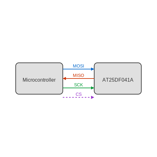
6.3 Case Studies in Real-World Implementations
The Serial Peripheral Interface (SPI) protocol has become vital in communication between microcontrollers and peripheral devices in modern electronics. This section explores several case studies that demonstrate the practical applications of SPI across various fields, highlighting how its implementation has solved specific challenges.
Case Study 1: SPI in Healthcare Devices
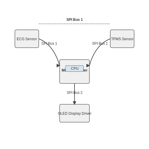
One significant application of SPI lies in the realm of healthcare monitoring systems. For instance, a team developing portable ECG monitors utilized SPI to handle communication between the microcontroller and various sensor modules. The ECG device required rapid data acquisition and processing, making SPI's high-speed capabilities beneficial.
The implementation allowed the sensor to transmit high-resolution data at speeds exceeding 1 MHz, thus providing continuous real-time monitoring. This system also featured a dual-channel setup where two SPI buses operated in parallel, significantly enhancing data throughput and ensuring accurate diagnostics. The robustness and simplicity of the protocol meant that power consumption remained low, crucial for battery-operated medical devices.
Case Study 2: Automotive Sensors
In automotive engineering, SPI plays a crucial role in various sensor applications, including wheel speed sensors and pressure monitoring systems. For example, an automotive manufacturer designed a tire pressure monitoring system (TPMS) that utilized SPI for inter-device communication among pressure sensors and the central processing unit (CPU).
Each tire sensor communicated via an SPI bus, allowing the CPU to receive tire pressure data promptly and reliably. The interruption-free communication provided by SPI reduced latency, enhancing the vehicle’s safety systems to react effectively to sudden pressure changes, thus ensuring real-time responsiveness. The data integrity ensured by SPI's synchronous nature was critical in mitigating the risks associated with under-inflated tires.
Case Study 3: Consumer Electronics
SPI is prevalent in consumer electronics, particularly within display technologies. A company developing high-resolution OLED displays used SPI for communication between the display driver IC and the microcontroller. The high data rates supported by SPI allowed for swift refreshing of pixels, improving the overall user experience.
The display system made use of multi-byte transfers and double buffering facilitated through SPI to prevent screen flickering during transitions. With a clock frequency set to 8 MHz, the design could drive the display at a frame rate suitable for video playback, showcasing SPI's versatility in various multimedia applications.
Conclusion
These case studies illustrate the SPI protocol's flexibility and high performance in real-world applications across multiple sectors—from healthcare to automotive dynamics and consumer electronics. Each implementation showcases how SPI not only enhances communication reliability and speed but also optimizes device performance and user experience, proving its essential role in modern electronic design.
7. Academic Journals and Articles
7.1 Academic Journals and Articles
- IEEE Transactions on Industrial Electronics — This article discusses the application of SPI protocol in industrial systems, highlighting its advantages in robust communication among microcontrollers.
- ScienceDirect Journal on Embedded Systems — This paper explores the use of SPI in embedded systems development, offering detailed experimental results on its performance.
- SAGE Journals on Sensor Networks — The study illustrates the integration of SPI protocol in sensor networks, focusing on energy efficiency and data integrity.
- ACM Digital Library on Communication Protocols — This research paper evaluates the SPI protocol within the context of communication protocols, with a critical analysis of its scalability and performance.
- Springer Journal on Advanced Automation — Offers insights into the role of SPI in automation systems, detailing case studies where SPI-based solutions improved system reliability.
- Physical Review B on Communication Systems — Provides a comprehensive review of SPI implementation in high-frequency communication systems, discussing theoretical underpinnings and practical execution.
- MDPI Sensors — This paper explores the use of SPI in enhancing sensor communication, with a focus on synchronization and data throughput optimizations.
- Wiley Online Library on Control Theory and Applications — Discusses the role of SPI in control applications, particularly in systems requiring precise timing and high-speed data transfer.
- Proceedings of the Institution of Mechanical Engineers, Part C — Examines the application of SPI in mechanical systems, showcasing innovative designs where SPI improves efficiency and data accuracy.
7.2 Online Resources and Communities
Navigating the intricacies of the SPI (Serial Peripheral Interface) protocol requires not just theoretical understanding but also practical insights, often best gleaned from active online communities and rich technical resources. Below is a curated list of online platforms that offer tutorials, forums, and detailed discussions about SPI and related technologies.- Microchip's Communication Design Center — This resource provides comprehensive guides on SPI application with examples, technical tips, and design support specifically for Microchip products. It offers detailed examples and downloadable resources to help with your implementation.
- Adafruit Learning System: SPI Protocol — Adafruit's tutorial on the SPI Protocol covers the basics and advanced topics with easy-to-follow examples and applications for hobbyists and professionals.
- Analog Devices Education Library — A vast library of educational materials including articles, tutorials, and webinars that delve into SPI communication among other industry-standard protocols, aiding engineers in designing robust systems.
- Texas Instruments SPI Solutions — This section offers a rich repository of documents, application notes, and design resources from Texas Instruments specific to SPI, aimed at supporting product development and innovative design solutions.
- Electronics Stack Exchange SPI Tag — A dynamic and collaborative Q&A platform where professionals and enthusiasts share their insights and troubleshoot SPI-related queries actively. It’s a great way to get peer-reviewed answers and practical advice.
- All About Circuits: Introduction to the SPI Protocol — This technical article provides an in-depth look at the SPI protocol, including its architecture, timing diagrams, and configuration settings with illustrative examples.
- Raspberry Pi Forums - Interfacing — A dedicated forum thread discussing interfacing techniques, including SPI, offering solutions and innovative ideas contributed by the Raspberry Pi community.
- SparkFun Learn: SPI Tutorials — SparkFun provides step-by-step tutorials covering SPI applications for various projects, useful for both beginner and experienced engineers aiming to enhance their practical understanding.
- Visual Studio Developer Community — For those coding and debugging SPI implementations in embedded systems using Visual Studio, this community offers tools, extensions, and collaborative spaces to solve complex software challenges.
7.3 Recommended Books and Textbooks
- Serial Peripheral Interface: Beyond the Basics — Authored by Gil Massobrio, this book delves into advanced topics of SPI, covering unique applications, circuit design insights, and the latest technological developments that can benefit both researchers and seasoned professionals.
- Introduction to Applied Digital Systems — Written by Jerry Twomey, this comprehensive text explores practical digital systems applications with a significant focus on protocols like UART and SPI, offering a robust blend of theory and practical guidance.
- Advanced Chip Design — Author Kishore K. Mullapudi presents strategies in integrated circuit design with extensive chapters dedicated to communication protocols such as SPI, highlighting real-world applications and problem-solving methodologies.
- Fundamentals of HDL Design — Sayfe Kiaei’s textbook provides a deep dive into hardware design languages with advice on implementing protocols like SPI in custom chip design, offering practical insights for engineering students and professionals.
- Embedded Systems Architecture — Authored by Tammy Noergaard, this resource tackles the architecture of embedded systems with a chapter dedicated to peripheral interfacing, including the detail-oriented workings of the SPI protocol.
- Digital Design and Computer Architecture — David Harris and Sarah Harris’ book meticulously explains digital systems, architecture, and interfacing, including comprehensive material on the SPI protocol's implementation in various computational environments.
- Serial Communications Using the Raspberry Pi — Warren Gay treats the applicability of the SPI protocol in the context of Raspberry Pi projects, illustrating practical projects and code snippets that benefit both enthusiasts and professional developers.
- Networked Embedded Sensing and Control — Editors Pengcheng Yi and Geir Hovland compile cutting-edge research related to embedded systems networking, with sections examining SPI in sensor data transmission and control systems.