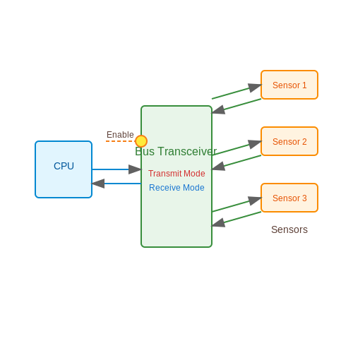
Decoding Protocols with Logic Analyzer
1. What is a Logic Analyzer?
1.1 What is a Logic Analyzer?
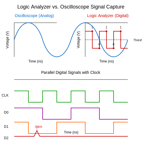
A logic analyzer is a crucial tool for engineers and researchers dealing with digital electronics. Its primary purpose is to capture and display multiple signals from a digital circuit, essentially allowing users to visualize the operation and interactions of complex digital systems. Unlike oscilloscopes, which focus on analog signals, logic analyzers are tailored for digital signals, often accommodating various protocols and data formats.
The device operates by sampling the digital signals at specific time intervals, storing the captured data, and decoding it for analysis. It can monitor multiple channels simultaneously—ranging from a few to several hundred—providing comprehensive insights into the state of a digital circuit at any given instant.
One of the most compelling advantages of a logic analyzer is its ability to trigger on specific events, allowing for precise debugging. This feature is vital in the rapid identification of issues in digital communication systems, microcontroller applications, and complex FPGA designs. As a result, logic analyzers are extensively used in industries such as telecommunications, automotive, aerospace, and consumer electronics.
Key Features of a Logic Analyzer
- Channel Count: Logic analyzers come with various channel counts, enabling them to monitor multiple signals, thereby making them suitable for complex systems.
- Sampling Rate: The sampling rate is critical as it determines how accurately the analyzer can reflect the state changes of signals. Higher sampling rates provide a better resolution of rapid signal transitions.
- Decoding Capabilities: Modern logic analyzers often have the ability to decode numerous communication protocols, such as I2C, SPI, UART, and even digital video interfaces, providing deeper insights into communication patterns.
- User Interface: The user interface of a logic analyzer is designed to aid in visualizing and analyzing waveforms effectively. Many devices allow for simultaneous display and comparison of multiple signal states.
The integration of software with hardware further enhances the capabilities of a logic analyzer. Desktop software can simulate complex database views of recorded data, providing engineers with statistical tools and waveform comparison features, ultimately aiding in quicker troubleshooting and optimization.
Real-World Applications
In real-world scenarios, logic analyzers are indispensable tools in various applications, including:
- Embedded System Development: They are often used to solve communication errors in embedded systems where multiple protocols may interact.
- Protocol Analysis: Logic analyzers enable the analysis of traffic between devices, helping engineers understand and debug communication issues.
- FPGA Design: When developing FPGA configurations, logic analyzers monitor outputs to ensure compliance with signal integrity standards.
Ultimately, a logic analyzer stands out as an essential instrument within the toolkit of any engineer working with digital electronics. It not only streamlines the debugging process but also enhances our understanding of intricate digital systems.
To summarize, the use of a logic analyzer transcends mere signal observation; it enables engineers to engage collaboratively with the intricate behaviors of digital circuits, leading to innovative designs and robust implementations.
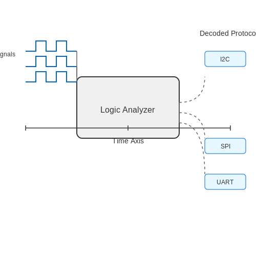
1.2 Key Components and Functionality
In the realm of digital electronics, a logic analyzer serves as an indispensable tool for examining and diagnosing digital signals. Understanding its key components and functionality lays the foundation for effective signal analysis. This section delves into the primary elements of a logic analyzer, their roles, and the practical applications they support.Core Components of a Logic Analyzer
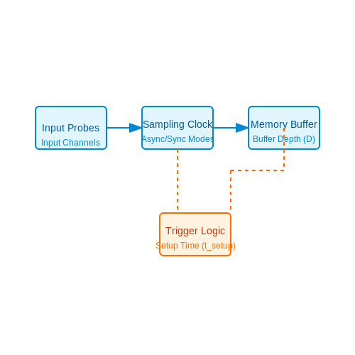
A logic analyzer consists of several crucial components that collectively enable it to capture, analyze, and display digital signals. The main components include:- Probes: These are the interfaces that connect the logic analyzer to the digital signals in the circuit. Probes can differ in type—some are passive, while others are active and can influence the signal. Careful selection is critical to ensure minimal signal distortion during measurement.
- Input Channels: Logic analyzers come equipped with multiple input channels, allowing them to simultaneously monitor several signals. The signal fidelity relies on the channel architecture, with differential pairs often used to reduce noise in high-speed applications.
- Sampling Rate: This defines how frequently a signal can be sampled by the logic analyzer. A higher sampling rate allows for a more accurate representation of high-speed signals. It's crucial to select a sampling rate that is at least twice the frequency of the highest signal being analyzed, adhering to the Nyquist theorem.
- Memory Depth: This parameter indicates how much data the analyzer can store for each input channel. Greater memory depth allows for longer observation times, which is essential when capturing sporadic events.
- Protocol Decoders: Many modern logic analyzers include built-in protocol decoders that translate the captured digital signals into human-readable formats. These decoders can recognize various digital communication protocols, adding considerable efficiency to the debugging process.
- Display Interface: The logic analyzer provides a visual interface for interpreting the captured signals. Advanced displays often allow for customizable visualization of the signal waveforms, offering quantitative and qualitative insights at a glance.
Functionality and Operations
The functionality of a logic analyzer is intricately linked to its components. When engaged, a logic analyzer performs several operations that contribute to effective diagnostics: 1. Signal Capture: The primary function of a logic analyzer is to capture digital signals from multiple points in a digital circuit. Utilizing its probes, the analyzer samples the voltage levels at specified time intervals across its channels. 2. Data Storage and Processing: Once signals are captured, they are stored in memory. The depth of this memory influences how much data can be recorded. High-frequency systems often require substantial memory depth to maintain detail over time. 3. Triggering: Triggering is a critical function that allows the user to specify conditions under which the analyzer will begin capturing data. This selective data capture can focus on specific events, such as rising edges or particular data patterns, facilitating the efficient isolation of issues in complex systems. 4. Decoding and Analysis: Once data is captured, many analyzers analyze the waveform data in real-time, decoding signals according to predefined protocols (like SPI, I2C, UART, etc.). The protocol decoder interprets the timing and logic details, presenting them in a format that is easier to analyze and troubleshoot. 5. Data Visualization: The processed data is subsequently displayed in various formats, such as waveform diagrams or state tables. These visual data representations are integral for engineers to diagnose problems quickly and effectively. In practice, logic analyzers are used extensively in embedded systems development, telecommunications, data communication, and digital system design. They help not only in debugging hardware but also in verifying the correct implementation of logic states in complex systems, maintaining high integrity across digital platforms. As we explore further sections, we will delve into the practical implementation of logic analyzers, illustrating how these tools can be leveraged for optimized performance in various engineering and research applications.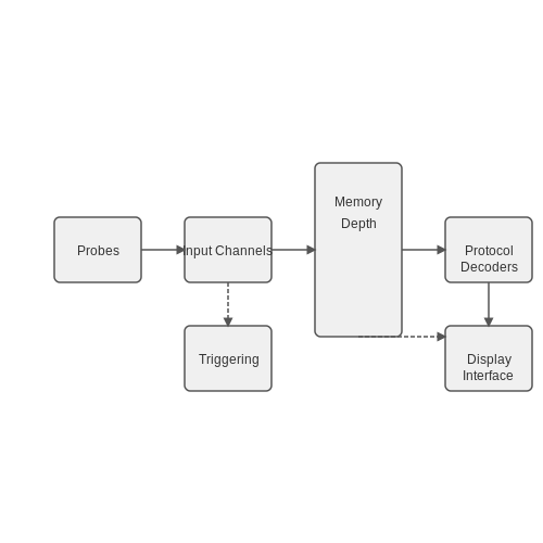
1.3 Types of Logic Analyzers
Logic analyzers have become indispensable tools in the realm of digital electronics and embedded systems development. These sophisticated devices can capture, display, and analyze complex digital signals, providing insights into the behavior of digital circuits. The understanding of the types of logic analyzers available is essential for engineers and researchers aiming to maximize their diagnostic capabilities. In this section, we will explore the various types of logic analyzers, discussing their features, applications, and practical relevance in today's technology landscape.
Overview of Logic Analyzer Types
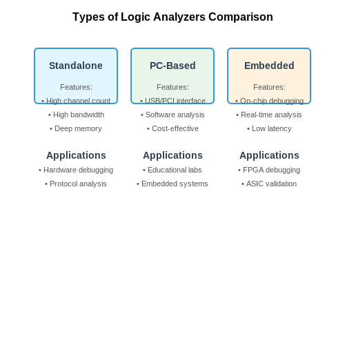
Logic analyzers can be categorized based on several criteria, including the technology they employ, the number of channels, their bandwidth capabilities, and their interface options. The primary types include:
- Standalone Logic Analyzers: These are dedicated hardware units designed specifically to analyze digital signals. They often come with multiple channels and are equipped with high sample rates, making them suitable for analyzing high-speed digital communication protocols.
- PC-Based Logic Analyzers: These devices connect to a computer via USB or Ethernet. While they may have a lower initial cost, they rely on the processing power of the connected PC for analysis, offering flexibility and advanced visualization features.
- Embedded Logic Analyzers: Often integrated into development boards or microcontrollers, these analyzers are designed for troubleshooting and debugging during the development phase. Their primary advantage is convenience, as they are typically used in conjunction with other hardware.
Standalone Logic Analyzers
Standalone logic analyzers are ideal for engineers requiring high bandwidth and numerous channels. They typically provide isolation from the PC environment, minimizing potential interference. These analyzers often feature dedicated interfaces for control, such as touch screens, knobs, and buttons, making them user-friendly.
Specifications and Use Cases
Consider a scenario in which a hardware engineer must debug a complex microcontroller system that communicates over multiple protocols simultaneously. A standalone logic analyzer can simultaneously monitor several data lines, enabling the engineer to inspect signals such as UART, SPI, and I2C without distorting the signal.
PC-Based Logic Analyzers
PC-based logic analyzers offer some unique advantages. Firstly, they leverage the computational power of modern PCs, providing the user with robust analysis and visualization capabilities. Users can utilize various software tools for deep analysis, including filtering, protocol decoding, and detailed signal charting.
Integration and Flexibility
For instance, a software package may allow users to customize the graphical display of captured signals, overlaying timing diagrams, or even applying custom scripts to offer unique insights. This flexibility is a significant advantage when troubleshooting intricate digital bus systems in professional environments.
Embedded Logic Analyzers
As we transition into the world of embedded systems, it's crucial to highlight embedded logic analyzers. These represent an innovative solution for engineers designing and testing applications in real-time. By integrating a logic analyzing capability inside a microcontroller, engineers can monitor signals without external equipment, streamlining the prototyping process.
Practical Applications
A perfect example is seen in automotive control systems, where embedded logic analyzers can be utilized to monitor various signal lines like CAN and LIN buses during live operation. This allows for immediate feedback and the ability to adjust control algorithms on the fly for optimized performance.
Conclusion
Understanding the types of logic analyzers equips engineers and researchers with the knowledge to select the appropriate tool for their diagnostics needs. By analyzing different types thoroughly and recognizing their strengths and weaknesses, users can enhance the efficiency of their development and troubleshooting processes.
2. Overview of Digital Communication
2.1 Overview of Digital Communication
In today's rapidly evolving landscape of electronics and communication, understanding the fundamentals of digital communication is essential. Digital communication refers to the process of transmitting data in a discrete form, which greatly differs from its analog counterpart. The shift from analog to digital signals marks a significant leap in efficiency, reliability, and scalability of communication systems.
At its core, digital communication enables the representation of information in binary format (0s and 1s), allowing for easier processing, storage, and transmission across various media. This representation supports a multitude of applications ranging from telecommunication and computer networking to data storage and multimedia services.
The Significance of Digital Encoding
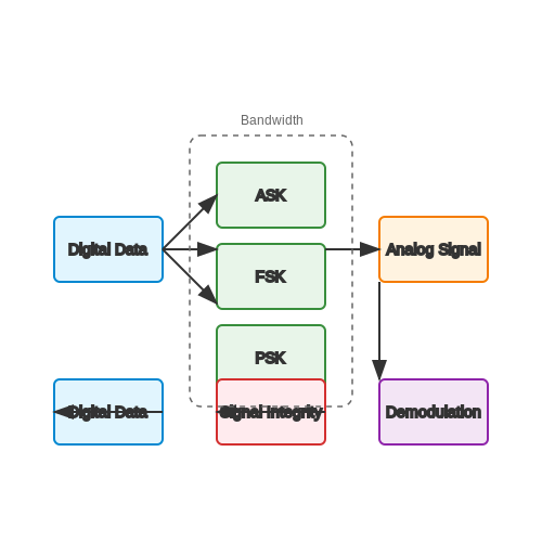
Digital encoding serves as the bridge between data and its transmission medium. The process often encompasses two fundamental components: modulation and demodulation. Modulation transforms digital data into analog signals suitable for transmission, while demodulation reverts the signals back into digital data for processing.
There are several modulation schemes employed in digital communications, including:
- Amplitude Shift Keying (ASK): Information is conveyed through changes in amplitude.
- Frequency Shift Keying (FSK): The frequency of the carrier wave is altered to represent data.
- Phase Shift Keying (PSK): Variations in phase are utilized to transmit data.
These schemes not only improve transmission efficiency but also enhance resilience to noise and interference, making digital communication significantly more robust compared to analog methods.
Signal Integrity and Bandwidth
Understanding the integrity of signals during transmission is crucial. Digital signals are less susceptible to degradation when compared to analog signals. Nonetheless, factors such as bandwidth and noise adversely affect digital communication systems. Bandwidth describes the maximum rate at which data can be transmitted, and it is imperative to optimize this to ensure high-quality signal delivery.
For advanced communication systems, concepts like Shannon's Theorem articulate the maximum data rate achievable over a noisy channel, thereby guiding engineers in system design. According to Shannon's formula:
Where C is the channel capacity in bits per second, B is the bandwidth in hertz, S is the average received signal power, and N represents the average noise power. This relationship elucidates the balance between bandwidth, signal quality, and communication efficacy.
Applications of Digital Communication
Digital communication systems have permeated virtually all aspects of modern life. They underpin technologies such as:
- Wireless and Cellular Networks: Facilitating mobile communication and data exchange.
- Satellite Communication: Enabling global data transmission.
- Internet Protocol (IP): Forming the backbone of data transfer across networks.
Additionally, the rise of the Internet of Things (IoT) and smart devices illustrates the growing reliance on digital communication infrastructures. Efficient data handling and scalability of these systems are crucial for future advancements in technology.
Through understanding the interplay of these concepts, engineers and researchers can leverage digital communication techniques to optimize performance, enhance signal integrity, and innovate new solutions within the realm of electronics.
2.2 Common Protocols and Their Applications
Logic analyzers serve as powerful tools for diagnosing and analyzing digital communication protocols. As engineers and researchers delve into the intricacies of embedded systems, a thorough understanding of common protocols becomes essential not only for troubleshooting but also for designing efficient communication architectures. In this section, we will explore several prevalent protocols and outline their practical applications, thereby enabling users to better utilize logic analyzers in their projects.
I2C (Inter-Integrated Circuit)
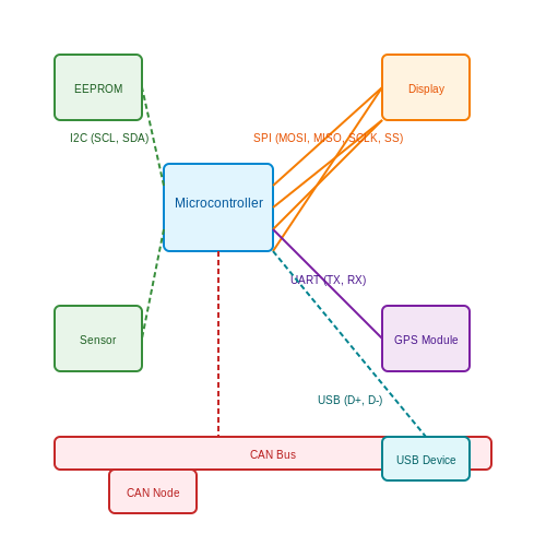
The I2C protocol is particularly notable for its simplicity and efficiency in inter-device communication. It allows multiple slave devices to be controlled by a single master via a two-wire interface (SDA for data and SCL for clock). This means that devices can communicate over short distances while minimizing pin usage, making it invaluable in compact circuit designs.
In practical applications, I2C is commonly used to connect sensors, EEPROMs, and even displays in embedded systems. When an engineer implements I2C, utilizing a logic analyzer to capture the clock and data signals can provide critical insights into the timing and conditions of the communication, helping troubleshoot failures when devices do not respond or data becomes corrupted.
SPI (Serial Peripheral Interface)
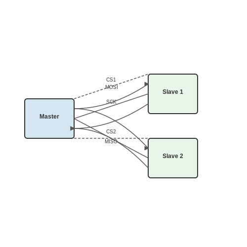
SPI is another widely used protocol, characterized by its high speed and full-duplex communication capability. It employs a master-slave architecture and typically involves four lines: MOSI (Master Out Slave In), MISO (Master In Slave Out), SCLK (Serial Clock), and SS (Slave Select). The reliance on individual slave select lines allows for the straightforward addition of multiple peripherals.
In real-world implementations, SPI is often favored in situations demanding fast data transfer rates, such as interfacing with memory cards and high-speed sensors. Logic analyzers play a crucial role in monitoring the integrity of the clock and data lines, ensuring that the expected timing and logical states match the system's specifications.
UART (Universal Asynchronous Receiver/Transmitter)
UART is notable for its simplicity and versatility, widely used for serial communication between microcontrollers, GPS modules, and Bluetooth devices. It functions asynchronously, which means that it does not require a shared clock between devices. Instead, it relies on a defined baud rate for timing synchronization.
The practical utility of UART is prominent in various applications, particularly in debugging and logging information from embedded devices. When a logic analyzer is employed to analyze UART communication, engineers can visualize waveform patterns, verify baud rates, and diagnose communication issues effectively, improving the design and reliability of serial interfaces.
CAN (Controller Area Network)
Designed for automotive applications, the CAN protocol is robust, allowing multiple microcontrollers to communicate with one another without a host computer. It adheres to a multi-master concept, where any node can send messages without waiting for a turn, prioritizing messages based on IDs to prevent collision.
The practical relevance of CAN is seen in modern vehicles, where various subsystems—such as engine control, braking systems, and infotainment—communicate through a central bus. By capturing CAN bus signals with a logic analyzer, engineers can troubleshoot issues in vehicle communication and ensure the correct operation of real-time systems.
USB (Universal Serial Bus)
USB has become the de facto standard for connecting various peripherals to computers. It supports both data transfer and power supply, and operates using a complex layer of protocols governed by the Universal Serial Bus Implementers Forum (USB-IF). Various speeds are supported, including USB 2.0, USB 3.0, and USB-C with significant advancements in data throughput.
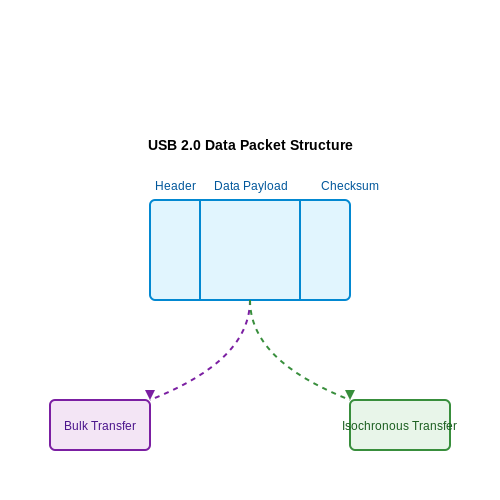
The ubiquitous nature of USB makes it essential in both consumer electronics and industrial applications. Logic analyzers can be invaluable in debugging USB communication issues, analyzing packet structures, and examining voltage levels to ensure compliance with the USB specification, thus enhancing device interoperability and performance.
Each of these protocols varies significantly in terms of architecture, speed, and application, reflecting the diverse requirements encountered in digital communications. By leveraging a logic analyzer to decode and analyze these protocols, engineers can enhance their understanding of complex systems and streamline their design processes, ultimately leading to more efficient and reliable electronic solutions.
2.3 The Importance of Timing in Protocols
In the intricate world of digital communication, protocols govern the rules and structure that ensure data is exchanged effectively. Central to the understanding of these protocols is the concept of timing, which plays a crucial role in determining the correctness and efficiency of data transmission. Timing refers to the precise intervals at which data is sent and received, and understanding it is paramount for engineers and researchers alike.
To grasp the significance of timing in protocols, one must consider the fundamental units of time that guide communication, such as clock cycles or baud rates. For instance, in a serial communication protocol like UART (Universal Asynchronous Receiver-Transmitter), timing is critical since the sender and receiver must agree on a specific baud rate. If the sending device transmits data at a different baud rate than the receiving device can process, data corruption is inevitable. Thus, the ability to analyze timing effectively becomes an invaluable skill for any electronic engineer.
Fundamental Timing Concepts
To appreciate the subtleties of timing in protocols, it's essential to understand several key concepts:
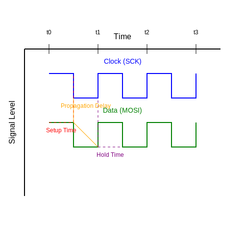
- Propagation Delay: The time it takes for a signal to travel from one point in a system to another. This delay impacts synchronous communications where devices need to operate in unison.
- Setup and Hold Time: The minimum time before and after the clock edge that data must be stable. Violating these times can lead to incorrect data being latched in flip-flops, ultimately resulting in system failures.
- Bit Timing: In protocols like I2C or SPI, each bit has a specific duration. Incorrect timing can lead to misinterpretation of data, as the receiving device may sample it at the wrong instance.
These fundamental concepts demonstrate that effective data communication relies heavily on accurate timing. A logic analyzer serves as an essential tool for engineers in diagnosing such timing issues. By capturing the digital signals over time, one can visually confirm that signals meet the required timing specifications defined by the respective protocols.
Analyzing Timing with a Logic Analyzer
A logic analyzer excels at capturing and displaying digital signals at high resolution over time. By setting up the device correctly, engineers can visualize signal transitions and compare them against timing diagrams found in protocol specifications. These diagrams show the expected timing relationships between clock signals and data signals. The analysis often involves looking for timing violations, such as data signals being sampled too early or too late relative to clock signals.
For instance, when analyzing a typical SPI communication, the logic analyzer can display the clock signal alongside the MOSI (Master Out Slave In) signal. By examining the relationship between these two signals, one can detect improper transitions that may lead to data corruption. This process is crucial in validating the integrity of communication systems, which is especially important in high-speed applications where timing margins are critical.
Real-World Application: Debugging Communication Interfaces
In practice, engineers often encounter timing-related issues when working with various communication interfaces in systems like microcontrollers, embedded systems, or computer networks. A classic example involves troubleshooting an I2C bus, where multiple devices may be connected. Due to capacitance on the bus line and variations in device response time, the timing can get skewed. Using a logic analyzer, technicians can visualize the bus transactions and identify faults in timing, allowing them to implement solutions such as bus pull-up resistors or modifying device firmware to optimize timing.
In conclusion, understanding the importance of timing in protocols is critical for ensuring reliable communication between devices. The use of a logic analyzer enhances an engineer's ability to troubleshoot and validate these timing aspects, greatly improving overall system performance and reliability. By developing a keen eye for timing relationships and employing appropriate tools, one can uncover hidden issues that may silently affect system operations.
3. Hardware Connections
3.1 Hardware Connections
When it comes to utilizing a logic analyzer for decoding protocols, the initial step involves establishing appropriate hardware connections. This foundational aspect is critical in ensuring that signals are accurately captured and analyzed. Understanding the intricacies of these connections optimally positions engineers and researchers to harness the full potential of logic analyzers in real-world applications.Understanding Logic Analyzers and Their Components
A logic analyzer is a sophisticated tool that captures and displays multiple signals from a digital system over time. The primary components of a logic analyzer include:- Probes: These are essential for interfacing with the digital circuit. They connect the logic analyzer to the circuit points where signals are to be monitored.
- Channels: A logic analyzer may have multiple channels, allowing it to capture several signals simultaneously, typically ranging from a few channels to hundreds of them.
- Decoding Capabilities: Integrated software algorithms can decode various protocols, making interpretation faster and more efficient.
Setup and Connections
Setting up a logic analyzer begins with selecting the right probes. Most analyzers come with differential or single-ended probes, depending on the signal type. Here is an overview of the setup process: 1. Choosing Probe Types: - Single-ended Probes: Suitable for capturing standard logic levels (0 and 1) where ground reference can be assured. - Differential Probes: Necessary for signals where noise could compromise the integrity, often used in high-speed communications. 2. Establishing Ground Reference: - A common ground connection is crucial. Connecting the ground pin of the logic analyzer to the system’s ground ensures that measurements are consistent and accurate. Failure to do so may introduce errors due to different ground potentials. 3. Signal Probing: - Connect the probe to the targeted pins of the circuit. It is advisable to minimize the length of the leads to reduce capacitance and inductance, which can lead to signal degradation. Careful attention should be paid to signal integrity—consider the rise and fall times of the digital signals. - For complex protocols, capturing a sync line can help in timing analysis. 4. Setting Voltage Levels: - Configure the input voltage thresholds on the logic analyzer, ensuring they correspond to the logic levels employed by the device under test (DUT). Most analyzers allow users to customize these thresholds through software settings. Here’s a simplified diagram of a typical hardware setup for a logic analyzer: This diagram illustrates a simple representation of how the logic analyzer probes connect to various points in the circuit. The connections may vary depending on the specific architecture and protocol under analysis but follow the same fundamental principles.Practical Considerations
Throughout this process, considerations related to the working environment should not be overlooked. Factors such as electromagnetic interference (EMI), temperature, and physical workspace can subtly influence measurement accuracy. If multiple devices are being analyzed simultaneously, employing isolation strategies—such as using shielded cables and avoiding cramped setups—can greatly reduce noise in the signals. In summary, a well-planned setup with appropriate hardware connections lays a solid foundation for successful protocol decoding using a logic analyzer. This knowledge finds practical applications in industries ranging from consumer electronics to aerospace engineering, where the performance and reliability of digital communications are paramount. As you align this foundation with your specific engineering tasks, it will refine your skills in signal interpretation, debugging, and overall system design.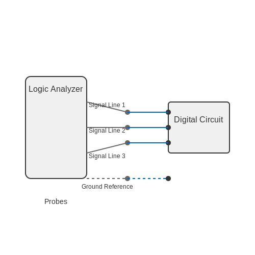
3.2 Software Configuration
The successful utilization of a logic analyzer hinges not only on its hardware capabilities but also significantly on the proper software configuration. This critical step involves both the setup of the graphical interface and the configuration of specific protocols to obtain precise data from the obfuscating noise of digital signals. Achieving optimal software configuration can transform raw data into actionable insights, making it invaluable for engineers engaged in digital design, debugging, and the research of communication protocols.Understanding Software Interfaces
Modern logic analyzers come equipped with sophisticated software interfaces that enable users to visualize, analyze, and interact with their data in various formats. Commonly, a logic analyzer's software interface consists of:- Waveform Viewer: Visual representation of logic states over time.
- Protocol Decoders: Tools that convert captured signals into human-readable formats.
- Trigger Setup: Allows users to specify conditions under which data capture is initiated.
- Export Options: Supports data exportation for further analysis in different formats, e.g., CSV, MATLAB.
Setting Up Protocol Decoders
Configuring protocol decoders is where a logic analyzer truly showcases its potency. The primary objective is to configure the software to recognize specific communication protocols, such as I2C, SPI, UART, or more complex standards like CAN or USB. Each protocol comprises its own distinctive characteristics and signaling methods, which the software can decode if set correctly. To initiate, you typically need to: 1. Select the Communication Protocol: Select the communication protocol you aim to analyze. This selection dictates how the software interprets the captured signals. 2. Define Timing Parameters: Accurately input timing parameters related to the bits' duration, clock frequencies, and sample rates. For example, in I2C communications, you might specify the bit rate, ensuring the logic analyzer samples at least 10 times the maximum rate of the communication. 3. Set Up Trigger Conditions: Establish specific triggering conditions that allow the system to capture relevant data. This might include setting flags for start or stop conditions and configuring the analyzer to capture data only when certain criteria are met, reducing noise and unrelated captures. 4. Validate the Configuration: Utilize visualization tools within the software to ensure the protocol is being captured as intended. Engaging graphical displays can offer immediate feedback about decoding accuracy.Practical Applications
The real-world applications of a well-configured logic analyzer are extensive. Engineers design intricate systems often favor protocol decoding in the validation of communication integrity across components. For instance, debugging an embedded system using SPI communication demands the analyzer be effectively configured to pinpoint errors such as misalignments in data packets. Let us consider a practical example involving the debugging of an I2C communication with an EEPROM: 1. Load the I2C protocol decoder in the logic analyzer software. 2. Set the sample rate to at least 10× the I2C clock frequency (e.g., for a 100 kHz I2C bus, use a sample rate of 1 MHz). 3. Configure the start and stop conditions to trigger data capture when an I2C read or write operation is initiated. The outcome is a visual representation of the communication, illustrating the actual bytes transmitted, significantly helping in quicker diagnostics and troubleshooting. In summary, the critical nuances involved in the software configuration of a logic analyzer form an integral part of any digital system design. From understanding user interfaces to the practical setup of protocol decoders, each step is pivotal in enabling engineers and researchers to derive meaningful insights from their signal analyses effectively. Moving forward, similar attention to detail will serve as the foundation upon which successful debugging and data analysis are built.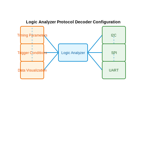
3.3 Calibration and Testing
In the realm of electronic diagnostics, particularly in decoding protocols with a logic analyzer, calibration and testing play crucial roles in ensuring accuracy and reliability. This section delves into the processes necessary for effective calibration and testing methodologies to optimize usage and performance of logic analyzers.
Calibrating the Logic Analyzer
Calibration is the process of adjusting the measurement capabilities of a logic analyzer to ensure that it accurately represents the signals being measured. There are several important steps to consider:
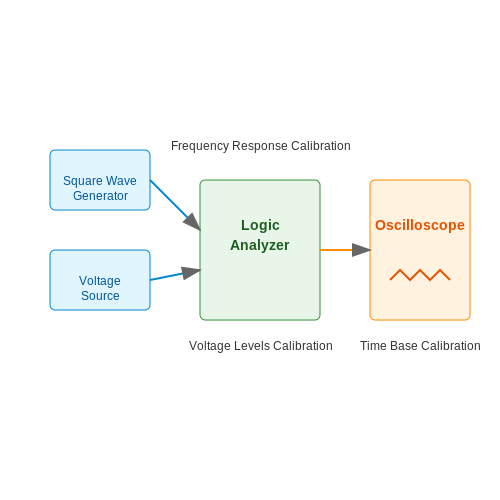
- Frequency Response Calibration: This ensures that the logic analyzer accurately measures signals across the intended bandwidth. A square wave generator, for example, can be used to check response at various frequencies. The output of the logic analyzer should match the expected output from the generator, which can be tracked with a precision oscilloscope.
- Voltage Levels Calibration: Settings should be adjusted to accurately interpret high and low voltage levels based on the specific logic family (e.g., TTL, CMOS). Calibration can involve applying known voltage levels to the inputs and verifying correct interpretation on the analyzer's display.
- Time Base Calibration: This ensures that time measurements taken by the logic analyzer are accurate. Using a precise time source, such as a pulse generator with a known frequency, calibration can help verify that timing characteristics, such as pulse width and interval, are measured correctly.
Once the calibration process is complete, it's prudent to perform a series of tests to verify calibration accuracy and functionality.
Testing Procedures
Testing is essential to confirm that the logic analyzer is functioning within its specified parameters. The following approaches are recommended:
- Self-Testing: Many modern logic analyzers include built-in self-test functionality to assess performance without external signals. Running these tests periodically can quickly identify hardware or software issues.
- Input Signal Testing: Use known signal sources to simulate real-world input conditions. This can include logic signals with variations in frequency, voltage levels, and signal shapes. By comparing recorded data to expected results, any inaccuracies in clipping, timing, or voltage levels can be detected.
- Multi-Channel Testing: Testing with multiple channels simultaneously allows for the evaluation of crosstalk, timing skew, and signal integrity issues. Recording and analyzing interactions between channels can reveal flaws in design or implementation that may not be apparent with single-channel tests.
Importance of Documentation and Analysis
Throughout the calibration and testing phases, maintaining rigorous documentation is vital. This includes keeping records of calibration results, testing conditions, and any deviations encountered. Such documentation not only enhances repeatability but also facilitates troubleshooting in the future. Data from these tests can be analyzed to yield insights into the logic analyzer’s performance over time, leading to better decision-making regarding when to recalibrate or replace equipment.
In practical applications, effective calibration and testing enhance the reliability of data captured during protocol decoding, particularly when working with complex systems involving hardware protocols and communication standards. This forms the groundwork for successful debugging and analysis, which is critical in fields such as embedded systems development, data communication, and modern digital circuit design.
4. Triggering Mechanisms
4.1 Triggering Mechanisms
In the realm of digital signal analysis, effective triggering is paramount for accurate and meaningful waveform capture with logic analyzers. The selection of a proper triggering mechanism can significantly influence the efficiency of data collection and ultimately the interpretation of serial communication. An in-depth understanding of triggering mechanisms not only enhances the precision of acquired data but also aids in diagnosing complex electronic systems.
Understanding Triggering in Logic Analyzers
Triggering refers to the defined conditions under which a logic analyzer begins its data acquisition process. This stage is critical because it ensures that the analyzer captures relevant segments of the digital signal while ignoring extraneous noise and irrelevant data. By specifying exact conditions for triggering, one can focus on events of interest, enhancing both the speed and accuracy of analysis.
Types of Triggering Mechanisms
Logic analyzers typically incorporate various triggering mechanisms, which can be broadly categorized into three main types:
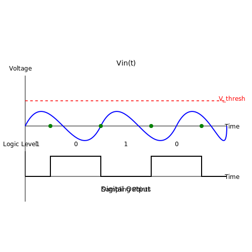
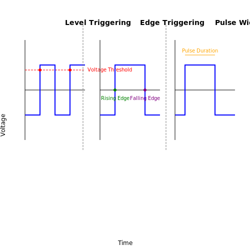
- Level Triggering: This mechanism activates data capture when a specific voltage level is reached or exceeded on one or more channels. For instance, you may set a threshold where the analyzer begins recording when an input signal rises above 2.5V. This approach is beneficial when monitoring signals for a defined high or low state.
- Edge Triggering: Edge triggering initiates data capture at a specific transition of a signal, either rising (positive edge) or falling (negative edge). This mechanism is widely used in digital systems where events are often characterized by transitions.
- Pulse Width Triggering: This triggering mechanism focuses on the duration of a pulse, allowing for the recording of pulses that exceed or fall short of a specific width. This is particularly useful in applications involving pulse modulation or in generating accurate timing measurements.
Setting Up Basic Triggering Conditions
To effectively utilize a logic analyzer, configuring triggering conditions is essential. Here’s a general approach to set up basic triggering conditions:
- Identify the signal of interest and determine its relevant characteristics—whether it is defined by its voltage levels, edges, or pulse widths.
- Access the triggering configuration menu on the logic analyzer. Most devices will provide an interface to set your desired conditions through either a graphical user interface or control knobs.
- Select the appropriate triggering mechanism. For instance, if you are interested in capturing the moment a signal transitions from low to high, opt for edge triggering.
- Specify the timing details, such as the threshold levels for voltage and the particular channels to monitor.
- Start the acquisition and evaluate the captured data, making adjustments as necessary to refine the accuracy of the signals being analyzed.
Real-World Applications of Triggering Mechanisms
The significance of effective triggering mechanisms in logic analyzers extends to numerous practical applications:
- Communication Protocol Analysis: In serial communications, triggering on specific protocol events aids in isolating message frames for protocols such as I2C, SPI, or UART, facilitating debugging and analysis of communication issues.
- Digital System Debugging: When diagnosing faulty logic circuits, edge or level triggering enables precise identification of anomalies in signal transitions or levels, crucial for engineers troubleshooting complex systems.
- Timing Analysis: Understanding the timing relationships between various signals is essential for synchronous systems. Pulse width triggering can assist in determining timing margins and ensuring system reliability.
In conclusion, mastering the triggering mechanisms of logic analyzers is essential for advanced electronic analysis. By appropriately configuring triggering conditions, one can significantly improve the efficiency of data acquisition and enhance the understanding of complex signaling behaviors.
4.2 Data Capture Techniques
In the realm of decoding protocols using logic analyzers, understanding various data capture techniques is paramount. These techniques not only enhance the fidelity of captured data but also optimize the analyzer’s performance in real-world scenarios. This section elaborates on the intricacies of these techniques, including their practical applications and implications in advanced electronic debugging and analysis.
Understanding Sample Rate and Bandwidth
Before delving into specific techniques, it’s crucial to grasp the relationship between the sample rate, bandwidth, and the signals being captured. The Nyquist Theorem states that to avoid aliasing—a phenomenon where higher frequency signals are misrepresented in digital samples—the sample rate must be at least twice the highest frequency component of the signal. For instance, if the highest frequency of interest in a captured signal is 20 MHz, the minimum sample rate should be 40 MHz.
This insight directly influences the logic analyzer’s design parameters; a higher sample rate enables better resolution and more accurate representations of fast digital transitions. Modern analyzers often exceed this threshold, allowing them to capture rapid digital signals with high fidelity. Therefore, selecting an appropriate sample rate is a foundational step for successful data capture.
Triggering Methods
One of the most powerful features of logic analyzers lies in their triggering capabilities. Triggering allows users to define specific conditions under which the analyzer begins capturing data, effectively honing in on the relevant events in a dataset. The types of triggering methods typically include:
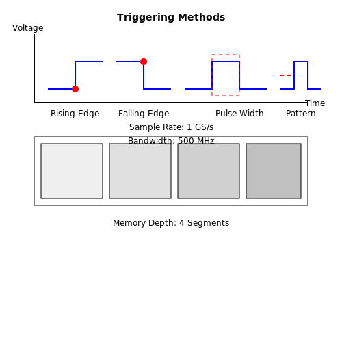
- Edge Triggering: Activates data capture on a specific signal edge—either rising or falling. This is the most common form of triggering and is suitable for observing digital signals’ transitions.
- Pulse Width Triggering: Initiates data capture based on the width of the detected pulses, allowing for analysis of pulse characteristics.
- Pattern Triggering: Captures data when a specific bit pattern is detected across the input channels. This is particularly useful for triggering on complex data protocols.
- Timeout Triggering: Starts data capture if a signal remains stable for a specified duration, thereby identifying potential system hang-ups or deadlocks.
Using Protocol Decoders
Advanced logic analyzers often incorporate built-in or external protocol decoders, further enhancing data representation and analysis. Protocol decoders take the raw data from the logic analyzer and translate it into higher-level protocol packets, allowing engineers to see the data in the context of the communication protocol being used, such as SPI, I2C, or UART.
By leveraging decoders, users can quickly isolate and interpret the significance of captured signals, enhancing debugging efficiency. These tools highlight important elements such as start and stop bits, as well as addressing and checksum checks, which are essential for protocol integrity.
Memory Depth and Data Overflow Techniques
Another critical aspect of data capture relates to the logic analyzer's memory depth. Memory depth refers to the amount of data that can be stored during a capture session. Digital signals can change states very rapidly, and without sufficient memory depth, signal integrity can be compromised due to data overflow.
Modern logic analyzers address this issue through advanced buffering techniques, where samples can be segmented and stored in blocks rather than a single contiguous buffer. This not only prevents overflow but also allows users to efficiently analyze large volumes of data. Users should always consider memory depth requirements based on expected signal activity and event durations to establish optimal configuration settings.
Conclusion: Optimizing Data Capture Techniques
To summarize, mastering data capture techniques is essential for effectively utilizing logic analyzers in protocol decoding. By adeptly manipulating the sample rate, employing sophisticated triggering methods, utilizing protocol decoders, and managing memory depth, engineers and researchers can enhance their ability to analyze complex digital systems. The implementation of these techniques not only streamlines the debugging process but also allows for meaningful insights into system performance and behavior.
4.3 Analyzing Captured Waveforms
Understanding the dynamics of captured waveforms is crucial for effectively decoding communication protocols using a logic analyzer. The ability to visualize and manipulate these waveforms allows engineers and researchers to identify signal integrity issues, timing discrepancies, and protocol compliance. In this section, we will delve into the various techniques for analyzing captured waveforms, the significance of waveform characteristics, and practical applications in real-world scenarios.
Interpreting Waveform Characteristics
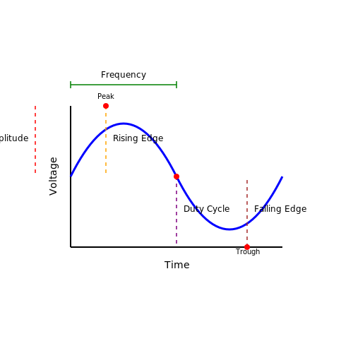
When analyzing waveforms, it is essential to grasp key characteristics such as amplitude, frequency, duty cycle, and edge timing. Each of these attributes provides insights into the health and integrity of the signal.
- Amplitude: The height of the waveform can indicate the strength of the signal. In digital systems, we typically compare the amplitude against defined thresholds, which characterize high and low logical states.
- Frequency: The frequency of the signal indicates how rapidly the waveform transitions occur. It can affect data rates in communication protocols; understanding frequency helps in debugging timing issues.
- Duty Cycle: This refers to the ratio of the active time of the signal to the total period. A duty cycle that is not within expected limits may indicate a problem in the transmitting device.
- Edge Timing: Analyzing the rising and falling edges of the waveform can reveal timing margins, setup time, and hold time violations, which are critical in synchronous systems.
Utilizing a Logic Analyzer for In-Depth Analysis
Logic analyzers provide tools for capturing, storing, and analyzing these waveforms in depth. Once the analyzer captures the waveform data, engineers can leverage its software to decode complex signals and visualize their timing relationships. This can be accomplished through features including:
- Triggering: Set specific conditions to start capturing data, such as a particular voltage level or a specific sequence of states.
- Decoding Protocols: Use the analyzer's built-in decoders designed for specific protocols, such as SPI, I2C, or UART. The analysis software interprets the waveform and presents it in a human-readable format.
Real-World Applications
The ability to analyze captured waveforms is not only essential during the development phase of hardware but also in field testing, debugging applications, and maintenance. For example:
- Signal Integrity Analysis: Analyzing captured data helps engineers identify reflections, crosstalk, and propagation delays that could lead to failures in communication.
- Protocol Debugging: By decoding waveforms from protocols such as I2C or SPI, engineers can ensure that devices communicate correctly and troubleshoot issues effectively.
Now that we have established the foundation of analyzing captured waveforms, the next step is to explore practical methods for visualizing these waveforms, further enhancing your analysis capabilities. The transition to this next topic will guide you through the procedures of using software tools and hardware interfaces to manipulate and observe these critical electronic signals.
5. Serial Communication (UART)
5.1 Serial Communication (UART)
Universal Asynchronous Receiver-Transmitter (UART) is a communication protocol utilized in many electronic systems for asynchronous serial communication. Unlike synchronous protocols, UART employs start and stop bits to delineate the boundaries of transmitted data, making it fundamentally simpler and ideal for various applications, including microcontroller interfacing, debugging, and telemetry systems.
Understanding UART Basics
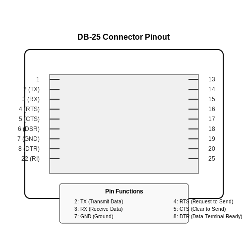
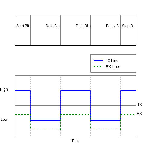
A UART setup typically involves two communication lines: one for transmitting (TX) and the other for receiving (RX). The data is sent as a series of individual bits over these lines, typically at a specified baud rate, which indicates the number of signal changes per second. A key feature of UART is its ability to operate without a shared clock signal; instead, both transmitting and receiving devices must be set to the same baud rate to ensure correct interpretation of the data.
The basic frame of a UART transmission consists of:
- Start Bit: A single bit indicating the beginning of transmission.
- Data Bits: Typically ranging from 5 to 9 bits, representing the actual binary data.
- Parity Bit: An optional bit used for error checking. Common configurations include even, odd, or none.
- Stop Bit: One or more bits signaling the end of the transmission.
In serial communication, the baud rate correlates directly with the bit duration, which must be consistent among all devices. For example, if a device is set to a baud rate of 9600, each bit's duration is approximately 104 microseconds. Understanding these parameters is crucial for successful data transmission without framing errors.
Decoding UART Signals with a Logic Analyzer
A logic analyzer is an invaluable tool for examining UART communication, as it allows engineers and researchers to visualize and interpret the digital signals transmitted over the TX and RX lines. When using a logic analyzer to decode a UART signal, users typically follow these steps:
- Connect the logic analyzer probes to the TX and RX lines of the UART interface.
- Configure the analyzer with the correct baud rate matching the UART setup.
- Initiate data transmission from the source device.
- Capture the waveforms and apply UART decoding features provided by the analyzer’s software.
Once configured, the logic analyzer will display the transmitted data in a human-readable format, significantly simplifying troubleshooting and analysis. The captured waveform will typically resemble a series of high and low signals, with the level transitions corresponding to individual bits.
Practical Applications of UART
UART is extensively used in various applications, ranging from low-level debugging of embedded systems to communication in advanced robotics and IoT devices:
- Microcontroller Interfaces: Many microcontrollers, like those from the Arduino platform, have built-in UART capabilities for Wi-Fi, Bluetooth, and other peripheral communications.
- Telecommunication Systems: UART protocols form the backbone of many telecommunication devices due to their simple wiring and robust nature.
- Debugging Tools: Development boards often use UART for serial console outputs, aiding in the debugging process by providing real-time status information.
The versatility and simplicity of UART make it an enduring choice for engineers, enabling reliable long-distance communication across multiple platforms. As embedded systems evolve, so too will the applications of UART, highlighting its relevance in contemporary electronics.
5.2 SPI Protocol Decoding
The Serial Peripheral Interface (SPI) protocol is a widely used synchronous serial communication interface, notable for its high-speed data transfer capabilities and flexibility. Developed by Motorola, it has become a standard for connecting microcontrollers to a range of peripherals, including sensors, displays, and memory devices. In this subsection, we will explore the core features of SPI, its architecture, and how to decode SPI signals using a logic analyzer.Understanding SPI Architecture
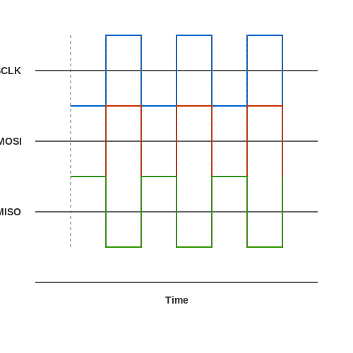
SPI operates in a master-slave configuration, where a single master device controls the communication with one or more slave devices. The architecture comprises four primary signals:- SCLK (Serial Clock): The clock signal generated by the master to synchronize data transmission.
- MOSI (Master Out, Slave In): The line through which the master sends data to the slave.
- MISO (Master In, Slave Out): The line through which the slave sends data back to the master.
- SS (Slave Select): This active-low signal is used by the master to select the specific slave device to communicate with.
Configuring a Logic Analyzer for SPI Decoding
To analyze and decode SPI signals with a logic analyzer, proper configuration is crucial. Follow these steps to set up your logic analyzer: 1. Connect the Logic Analyzer: Ensure that the SCLK, MOSI, MISO, and SS lines from the SPI bus are connected to the corresponding capture channels on the logic analyzer. It is essential for grounding to be uniform to avoid reference issues. 2. Set the Sample Rate: Configure the logic analyzer’s sample rate to be at least 4-5 times higher than the maximum expected SCLK frequency. This oversampling ensures accurate capture of the signal. 3. Select SPI Protocol Decoder: Most modern logic analyzers come equipped with protocol decoder functionalities. Select the SPI protocol decoder in your software to facilitate automated decoding of the captured signals. 4. Capture the Data: Initiate the data transfer by triggering the SPI communication. This could be as simple as initiating a read or write command from the master.Decoding SPI Signals
After capturing the SPI signals, the logic analyzer will provide a visual representation of the communication. The key points to observe during the decoding process include: - Clock Signal Alignment: Ensure that data bits are sampled on the correct clock edge (either the rising or falling edge, depending on the configuration). - Data Alignment: Observe the timing between the SCLK and the MOSI/MISO lines to confirm that the data is being transmitted correctly during the clock cycles. The visual display on the logic analyzer will depict timing diagrams where transitions correspond to clock signals and data bits. The cleaner the signal (i.e., less noise and clearer edges), the more accurate the interpretation will be. To visualize an SPI waveform, consider a timing diagram that illustrates the relationship between the SCLK, MOSI, and MISO signals: A comprehensive study of these signals informs you not only of successful communication but also aids in debugging, allowing for timely detection of communication errors inherent in SPI transmission.Practical Applications of SPI
SPI's inherent characteristics make it suitable for various applications such as:- Communication with Sensors: Many sensors and modules (e.g., ADC, DAC) utilize SPI for high-speed data acquisition.
- Memory Interfacing: Flash and EEPROM memory often employ SPI for quick read/write operations, making them ideal for embedded system storage.
- Display Control: TFT displays typically use SPI to enable rapid graphical interface manipulation.
5.3 I2C Protocol Analysis
The Inter-Integrated Circuit (I2C) protocol is a widely used communication interface that enables multiple slave devices to be controlled by a master using only two wires: the Serial Data Line (SDA) and the Serial Clock Line (SCL). Understanding the I2C protocol is essential for engineers and researchers who work on embedded systems, sensor networks, and other applications requiring efficient inter-device communication.Operational Overview of I2C
Developed by Philips Semiconductors in the early 1980s, I2C stands out for its simplicity and versatility. It supports various devices on a single bus and allows for easy addition of multiple slaves without the need for additional hardware. Each device on the bus has a unique address, typically 7 or 10 bits long, which the master device uses to communicate with the intended slave. This addressing scheme reduces bus contention while enabling devices to share the I2C bus. The protocol utilizes a master/slave architecture wherein the master initiates communication and controls the clock signal, while slaves respond to the master's requests. The communication occurs in data frames, which include start conditions, data bytes, acknowledgment bits, and stop conditions.Real-World Applications
I2C finds extensive use in low-speed and medium-speed data transmission applications, including:- Microcontroller peripherals: Many microcontrollers integrate I2C for interfacing with sensors, EEPROMs, RTCs (Real-Time Clocks), and displays.
- Consumer electronics: Devices like TVs and cameras utilize I2C for controlling internal functions and communicating with different modules.
- Automotive systems: Modern vehicles leverage I2C for communication between various sensors and control units, enhancing performance and safety.
Decoding I2C Signals with a Logic Analyzer
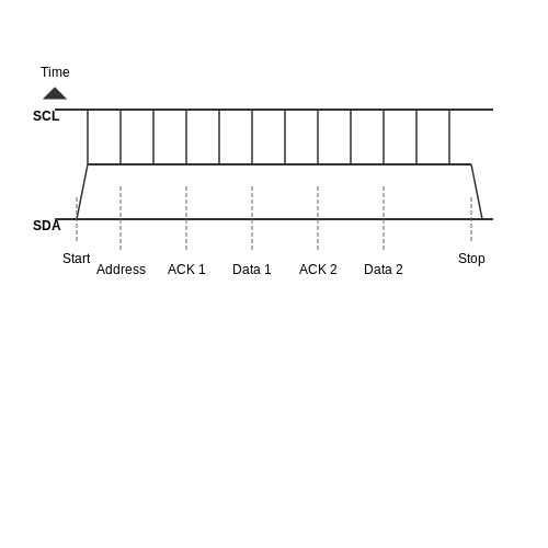
Using a logic analyzer for I2C protocol analysis provides a visual and systematic way to observe and decode the communication signals. The analysis process begins by connecting the logic analyzer's probes to the SDA and SCL lines of the I2C bus. The following steps outline the typical workflow for decoding I2C signals: 1. Set up the logic analyzer: Configure the channels to capture the SDA and SCL lines while selecting the I2C protocol for automatic decoding. Ensure that the sample rate is set adequately; ideally, it should be at least four times the highest frequency of the I2C clock to capture the details accurately. 2. Start the communication: Trigger the logic analyzer to start capturing data when a START condition is detected. In an I2C protocol, a START condition occurs when the SDA line goes low while SCL is high, indicating the beginning of a transmission. 3. Analyze the protocol frames: Examine the captured waveform in the logic analyzer's software. The graphical representation will clearly show the sequence of data transmitted, the acknowledgment bits from slave devices, and whether the communication terminates with a stop condition. 4. Understand the I2C frames: Each I2C frame consists of: - A START condition - 7 or 10-bit address and read/write bit - Data bytes (in 8-bit segments) - Acknowledgment (ACK or NACK bit) - STOP condition. Utilizing these factors will allow you to interpret the captured data effectively.Interpreting Results
When analyzing I2C communications, special attention needs to be paid to timing. Key parameters include: - Clock Frequency: Common I2C speeds are 100 kHz (standard mode) and 400 kHz (fast mode), although high-speed modes can reach up to 3.4 MHz. - Data Hold Time: After the SCL goes high, the data on SDA should remain stable for at least a specified time interval. - Data Setup Time: Before SCL goes high, SDA should be stable for a certain period to ensure proper reading. Decoding these parameters provides insights into potential issues such as signal degradation, timing violations, and so forth. In summary, I2C protocol analysis via a logic analyzer is a robust process catering to a multitude of applications in engineering and technology. Mastery of these techniques not only enhances diagnostic capabilities but also fosters innovation in system design and development.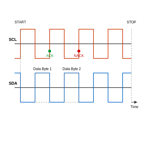
6. Custom Protocol Decoding
6.1 Custom Protocol Decoding
Introduction to Custom Protocol Decoding
In the realm of embedded systems and electronic communication, the ability to decode custom protocols is invaluable. A logic analyzer serves as a powerful tool for this purpose, enabling engineers and researchers to visualize, decode, and analyze data streams that do not conform to standard protocols, such as I2C, SPI, or UART. This subsection delves into the methods for creating custom decoding algorithms tailored to specific communication protocols, which can be highly unique to particular applications.
Understanding the Basics of Signal Interpretation
Before diving into custom protocols, it's essential to grasp the fundamental principles of signal interpretation that logic analyzers employ. At its core, a logic analyzer captures digital signals and displays them in a time-correlated format, enabling detailed analysis. Each bit of data can represent a state or command in a protocol. The effectiveness of custom protocol decoding hinges on correctly mapping these bit transitions to meaningful command structures and payloads.
When dealing with non-standard protocols, one often encounters challenges such as variable bit lengths, different signaling techniques, or non-volatile state machines. Therefore, defining the protocol's structure, including start bits, stop bits, data length, and any control bits, is crucial for successful decoding.
Defining the Custom Protocol
To begin creating a custom decoding scheme, follow these steps:
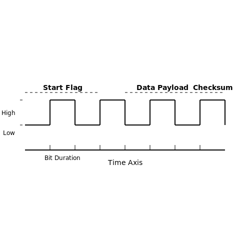
- Specify the Protocol Structure: Understand the data format. For example, a hypothetical protocol might consist of a 1-byte start flag, followed by a variable-length data payload and a 1-byte checksum.
- Identify Timing Requirements: Specify the timing for valid signal states, including rise and fall times as well as the overall duration of a bit transmission.
- Error Detection and Handling: Implement mechanisms for identifying erroneous transmissions, such as checksum validation or bit pattern verification.
Implementing the Decoding Logic
With the protocol structure firmly established, the next step involves implementing the logic that translates captured signals into meaningful data. Most logic analyzers provide a scripting or language interface for custom definitions. For example, let’s consider simple pseudocode that outlines this process:
In this pseudocode:
- The logic iterates through each captured signal, checking for the defined start flag of the custom protocol.
- Upon detecting this flag, it proceeds to read the determined length of the data payload, followed by the payload itself.
- Checksum verification ensures data integrity before adding valid entries to the final output list for further analysis.
Real-World Applications
Custom protocol decoding is prevalent in various electronics applications. For instance, proprietary communication protocols in industrial IoT devices often require bespoke logic definitions for proper analysis. Moreover, debugging and testing electronic components can greatly benefit from such tools to ensure adherence to specific signal specifications, thereby enhancing development productivity.
In the automotive industry, custom protocol decoding helps engineers inspect communication between various electronic control units (ECUs). Here, data consistency can be critical for vehicle safety systems, making accurate decoding essential.
Conclusion
The capacity to decode custom protocols using logic analyzers not only adds a powerful tool to an engineer's toolkit but also opens doors to deeper insights into electronic communication. By defining the protocol, understanding its intricacies, and implementing robust decoding logic, one can achieve a comprehensive understanding of signal behavior within custom applications.
6.2 Troubleshooting Signal Integrity Issues
Signal integrity issues can severely compromise the reliability of digital communications. The role of a logic analyzer extends beyond mere data capture; it is pivotal in diagnosing these integrity problems that stem from physical characteristics of the signal and the environment in which it operates. In this segment, we will explore common signal integrity pitfalls and how to employ a logic analyzer effectively to identify and remedy these issues.
Understanding Signal Integrity
Signal integrity pertains to the quality of the electrical signals as they travel through a circuit. When signals lose their shape or integrity, it can lead to erroneous data being interpreted by the receiving unit. This degradation may arise from several factors, including noise, crosstalk, and reflections. Each of these aspects can distort the intended signal waveform, ultimately causing data errors.
- Noise: Unwanted variations in voltage or current that can superimpose on the desired signal. Common sources include electromagnetic interference (EMI) from nearby components and thermal noise.
- Crosstalk: Inductive or capacitive coupling between signal lines where one signal inadvertently affects another, leading to erroneous conditions.
- Reflections: Occur when there is an impedance mismatch in the transmission path, causing portions of the signal to reflect back towards the source.
Utilizing Logic Analyzers
When addressing signal integrity issues, a logic analyzer serves as an invaluable tool due to its capacity to visualize digital signals with time resolution. With its capability to capture multiple channels simultaneously, engineers can examine the relationships between different signals, allowing for detailed analysis.
The first step in troubleshooting is to establish a baseline performance. Using the logic analyzer, observe the ideal signal waveform in a controlled scenario. This reference will serve as a comparison against subsequent analyses. The following aspects are critical when interpreting the results:
Waveform Analysis
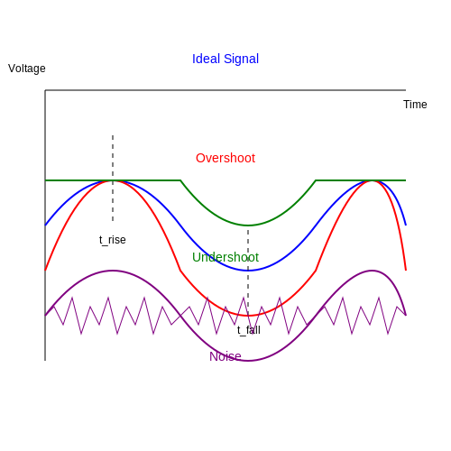
Analyzing the captured waveforms is central to identifying integrity issues. In an ideal scenario, the signal should exhibit clean transitions between logic levels. Deviations in rise time, fall time, and significant noise components can provide immediate clues to underlying problems. For instance, if a logic level transition is excessively slow or noisy, this might indicate excessive capacitance or high impedance in the circuit.
Where \(t_{rise}\) is the rise time, \(R\) is the resistance affecting the signal, and \(C\) is the load capacitance. Understanding this relationship helps assess whether components in your circuit contribute to poor performance.
Identifying Common Issues
Using the logic analyzer, a few common issues should be examined:
- Overshoot: When the signal exceeds the maximum voltage level before stabilizing. This can cause false triggering of digital logic levels.
- Undershoot: Similar to overshoot but occurs below the minimum voltage level, which can lead to latch-up conditions or component damage.
- Timing Violations: Irregularities in signal timing can indicate problems such as clock skew or delay that can disrupt synchronous communications.
Best Practices for Signal Integrity
To ensure optimal signal integrity, consider the following best practices when using a logic analyzer:
- Use proper grounding: Ensure that all grounds are connected to create a common reference point and minimize ground loops.
- Keep signal lines short: This reduces the risk of introducing capacitance and inductance that can affect signal quality.
- Use differential signaling: If noise is an issue, employing differential pairs can cancel out common-mode noise effectively.
By analyzing signal integrity quantitatively and qualitatively using a logic analyzer, engineers can diagnose underlying issues in high-speed digital systems and increase the reliability of their designs. Understanding these key principles of troubleshooting can lead to more robust electronics and better overall system performance.
6.3 Analyzing Timing and Synchronization
In the realm of electronic communication, understanding timing and synchronization is pivotal for decoding protocols effectively. Timing analysis involves scrutinizing the intervals between signal transitions, while synchronization ensures that devices operate in harmony within a specific protocol. With the aid of a logic analyzer, we can explore both concepts in depth, providing insights that are essential for advanced applications in digital systems design.Understanding Timing Analysis
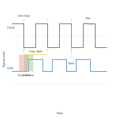
Timing refers to the precise measurement of the time intervals between signal events. In digital electronics, every signal change holds significance, and the ability to quantify these changes can greatly enhance one’s understanding of a protocol's performance. To analyze timing, we measure parameters such as setup time, hold time, and pulse width: - Setup Time: The minimum time a data signal must be stable before a clock edge. - Hold Time: The time a data signal must remain stable after a clock edge. - Pulse Width: The duration for which a signal remains high or low. Utilizing a logic analyzer, engineers can visualize these timings in a waveform display. For instance, a zoomed-in view on a clock signal can reveal the intervals between rising and falling edges, shedding light on whether the setup and hold times are met.Synchronization Fundamentals
Synchronization ensures that signal changes among different devices occur at the correct time, allowing coherent communication between components. In asynchronous systems, devices operate independently, while synchronous systems rely on a clock signal to align operations. The role of a logic analyzer becomes significant when diagnosing synchronization issues. By observing timing relationships between signal lines, one can identify skew—a condition where signals reach their destination at varying times due to differences in path lengths or transmission delays. Such discrepancies can lead to miscommunication and are critical to rectify for reliable circuit operation.Practical Applications in Protocol Decoding
Timing and synchronization are particularly relevant when working with communication protocols like SPI (Serial Peripheral Interface) or I2C (Inter-Integrated Circuit). For example, when decoding an I2C transmission, a logic analyzer can capture the start condition, address frame, acknowledgment bits, and stop condition. Analyzing the durations of these frames can help verify compliance with the protocol specifications. In real-world applications, issues such as clock drift or jitter can cause significant performance degradation. Here, a deep dive into timing analysis can reveal the root causes. For instance: - Clock Drift: A gradual shifting of clock signal timing independent of the actual data signals. This can cause synchronized systems to lose their alignment unless corrected through recalibration. - Jitter: The variability in signal timing that can introduce errors in data interpretation. By measuring the time between multiple similar signal transitions, one can quantify jitter and its effects on overall system performance.To summarize, effective timing and synchronization analysis using a logic analyzer not only aids in protocol decoding but is also crucial in ensuring that electronic systems operate reliably and efficiently. The ability to assess signal timings and synchronize operations has far-reaching implications in the fields of communication, control systems, and embedded design.
7. Real-world Applications of Logic Analyzers
7.1 Real-world Applications of Logic Analyzers
Logic analyzers have become indispensable tools in the realm of electronics and communication, enabling engineers and researchers to visualize and analyze digital signals with precision. Their capability to decode complex protocols opens the door to a range of real-world applications. In this section, we will explore various domains where logic analyzers prove their mettle, enhancing design, testing, and troubleshooting processes.Debugging and Development of Embedded Systems
In embedded systems design, where microcontrollers and digital logic circuits are prevalent, logic analyzers play a vital role. The debugging process often involves monitoring communication between different modules or devices. By capturing data streams, engineers can visualize the timings and verify signal integrity against expected waveforms. This enables rapid identification of issues, such as communication errors or latency problems. For instance, when working with I²C protocols in a microcontroller application, the logic analyzer can decode the bus activity, depicting the data bytes and acknowledge signals in real-time. By correlating this information with the system's operation, engineers gain insights that facilitate adjustments and optimizations.Verification of Communication Protocols
As the digital landscape evolves, communication protocols also become increasingly sophisticated. Logic analyzers facilitate the verification of these protocols—such as SPI, UART, and CAN—by decoding the signals into human-readable formats. This capability allows engineers to assert that their implementations conform to established standards. Technicians may find themselves in a situation where specific packet structures need to be verified. The logic analyzer graphically represents the packet data, helping them discern any discrepancies in payload size, addressing, or timing. By doing so, they can ensure compliance with the communication protocol specifications, thus maintaining product reliability.Automotive Electronics Testing
In the automotive industry, the integration of multiple electronic control units (ECUs) has compounded the complexity of vehicle systems. Logic analyzers are increasingly employed to diagnose and analyze the intricate timing relationships and data transfers between these ECUs. Advanced driver-assistance systems (ADAS) utilize multiple sensors and cameras that frequently communicate over high-speed serial interfaces. Analyzing those communications to ensure proper operation is crucial in preventing malfunctions that could lead to safety concerns. By deploying a logic analyzer, engineers can verify the timing and integrity of the data, ensuring optimal performance.Consumer Electronics Debugging
The consumer electronics sector, including smartphones and smart home devices, greatly benefits from the use of logic analyzers in the debugging phase. These devices often leverage complex digital communication protocols and require tight integration between hardware and software. For example, during the design of a new smart thermostat, engineers can use a logic analyzer to monitor the data exchange between the device and a central hub. This allows them to identify communication lags and enhance firmware before the product reaches the market, ensuring a seamless user experience.Airborne and Space Systems
Work in aerospace frequently demands a high degree of reliability, where systems must withstand extreme conditions while performing flawlessly. Logic analyzers are employed for the assessment of communication between various avionics systems, including flight control systems and communication satellites. The ability to monitor and decode high-speed signals through complex protocols like ARINC 429 and CAN is invaluable. Engineers utilize logic analyzers to streamline the testing phase, ensuring all signals meet rigorous standards and function as intended under demanding flight conditions.Conclusion
The applications of logic analyzers in real-world scenarios showcase their versatility and necessity in modern electronic design and troubleshooting. By effectively decoding digital protocols and providing real-time visualization of data paths, logic analyzers significantly enhance the efficiency, reliability, and performance of electronic systems across various industries. As technology continues to evolve, so too will the critical role of logic analyzers in ensuring seamless communication and operation within complex electronic architectures. The next section will delve into the methodologies for effectively utilizing logic analyzers for specific protocol decoding tasks, building upon the concepts discussed here.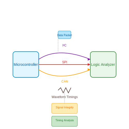
7.2 Common Pitfalls and How to Avoid Them
When utilizing a logic analyzer to decode communication protocols, engineers and researchers often encounter a variety of challenges that can obscure the insight provided by the acquired data. Understanding these common pitfalls and their prevention is critical for effective analysis. Below, we explore typical areas where mistakes occur and present strategies to mitigate these issues.Signal Integrity Issues
One of the foremost challenges faced during the decoding process is related to signal integrity. External factors such as noise, ringing, and crosstalk can distort the data capturing process. These distortions often lead to false triggering or incorrect data interpretation. To mitigate these issues, follow these best practices: - Utilize short and well-shielded cables to minimize interference. - Employ terminators to prevent reflections in high-speed signals. - Adjust the threshold levels on the logic analyzer to optimize data capture sensitivity.Timing Errors
Timing discrepancies can emerge from improper sample rates or setups that fail to match the data rate of the protocol being analyzed. An insufficiently high sample rate may lead to aliasing, while a sample rate that is too high can lead to redundant data and unnecessary processing. To avoid timing errors: - Calculate the Nyquist theorem requirement to establish an appropriate sample rate, ideally set continuously at least twice the maximum frequency of the signal. - Regularly calibrate your logic analyzer to ensure synchronization with other system components.Wrong Protocol Selection
Selecting the wrong protocol setting on the logic analyzer is a surprisingly common oversight. Each protocol has distinct characteristics in terms of frame structure, timing, and representation. To alleviate this issue: - Always verify the communication protocol and its parameters before capture, including baud rates, parity, and stop bits. - Review the protocol configurations off-line against the established specifications to ensure the correct interpretation of the subsequent waveform.Inadequate Grounding
Poor grounding can introduce noise into the measurement systems. This issue often manifests as bizarre glitches in the waveform and can propagate errors in data decoding. To strengthen grounding strategies: - Ensure your logic analyzer’s ground is connected to the same ground plane as the circuit under test. - Utilize differential probes when analyzing signals characterized by significant ground potential differences to ensure accurate readings.Data Overload and Management
With modern logic analyzers supporting high data rates and long capture durations, the volume of data may become overwhelming. Insufficient data management strategies can lead to delayed analyses or missed signals. To work through data overload effectively: - Implement filtering strategies within the logic analyzer to focus on specific channels or types of data. - Use software tools to pre-process or analyze the data stream, allowing for selective viewing of critical information.Neglecting Post-Capture Analysis
Finally, overlooking the importance of post-capture analysis can lead to misinterpretations. Waveform anomalies might indicate issues at various system stages that require further investigation beyond immediate decoding. To enhance post-capture analysis: - Leverage advanced analytics tools capable of comparing captured data to known good signal references. - Document findings for future reference and learning, which assists in building a knowledge base to contribute to troubleshooting efforts. By acknowledging these common pitfalls, practitioners can significantly enhance their proficiency with logic analyzers and improve the robustness of their analysis. Awareness of these challenges encourages proactive problem-solving, which is the hallmark of advanced engineering practices.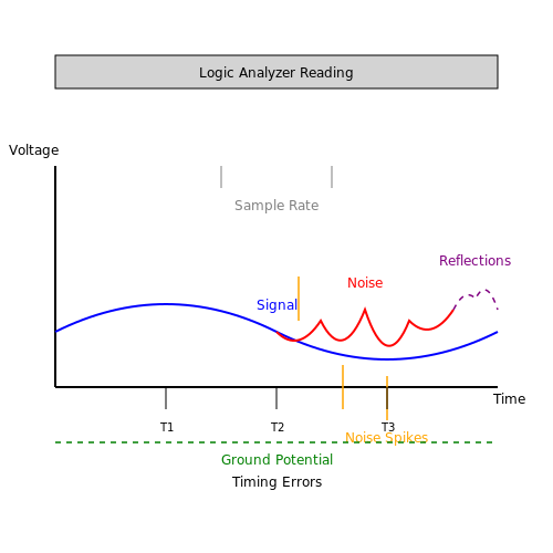
7.3 Best Practices for Effective Decoding
In the realm of digital electronics and data communication, using a logic analyzer is an invaluable asset for both development and debugging. The effectiveness of this sophisticated tool greatly hinges on the following best practices, ensuring accurate decoding and insightful analysis of digital signals.Understanding Signal Integrity
One of the cornerstones of successful decoding is maintaining signal integrity. Before any decoding process, verify that the signals being measured are clean and within specification. Noise, ringings, or reflections on the digital lines can introduce errors in the interpretation of logic levels. To mitigate these issues, consider using short connection leads and appropriate termination resistors per signal line specifications.Correct Trigger Settings
Proper trigger settings are crucial to capture the desired signal without spurious data. The choice of trigger condition should correlate closely with the expected data flow. Utilizing edge triggering based on specific signal transitions can help isolate relevant data packets. For complex protocols, it is often advantageous to delve into advanced triggering capabilities, such as pattern or pulse width triggering.Accommodating Protocol Variations
When decoding protocols, be cognizant of the potential variations that may exist within standards. For example, I2C can operate at different clock rates and use multiple addressing strategies, depending on the specific use case. Ensuring that the logic analyzer's decoding configuration matches the specific setup you're working with is essential. Detailed protocol documentation is invaluable, offering insights not only on standard operating characteristics but also on exceptions and custom implementations.Leveraging the Analyzer's Decoding Features
Most modern logic analyzers come equipped with advanced decoding features capable of interpreting many protocols directly. Familiarize yourself with these functionalities, such as automatic packet recognition, which can significantly save analysis time. The capability to enable or disable specific decoding options allows tailored analysis focused on observed phenomena rather than irrelevant data.Utilization of Data Visualization Techniques
Visualization plays a pivotal role in data interpretation. Make use of graphical representations available in your logic analyzer’s software. Timing diagrams, state tables, and protocol specific displays can enhance intuitive understanding. These visual tools can often reveal issues, such as timing violations or data corruption, that might not be readily apparent in raw binary or hexadecimal forms.Iterative Testing and Validation
Lastly, consider the value of iterative testing. Running multiple tests while altering conditions — such as voltage levels, environmental factors, and protocol configurations — can yield rich data sets and improve understanding of failure modes. Documenting these findings enables developing robust fixes and contributes to improved system design in future implementations. By adhering to these best practices, engineers and researchers can significantly enhance the efficiency and effectiveness of decoding protocols with logic analyzers, ensuring a smooth workflow from design through debugging phases. Whether you're testing a simple Arduino project or a complex communication system, these guidelines will streamline your methodology and improve your results.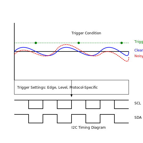
8. Recommended Textbooks
8.1 Recommended Textbooks
- The Art of Electronics by Paul Horowitz and Winfield Hill — This textbook is a comprehensive guide to electronic circuit design, often considered a foundational resource for engineers. It covers both the theoretical and practical aspects of electronics, making it ideal for understanding the intricacies of logic analyzers.
- Designing Analog Chips by Hans Camenzind — A resourceful book for those interested in analog electronics design, including explanations on how these principles integrate into digital systems where logic analyzers are used to monitor signals.
- Digital Design and Computer Architecture by David Harris and Sarah Harris — This text provides an in-depth exploration of digital circuits and architecture, giving readers a solid foundation in the logic systems often analyzed with logic analyzers.
- Microelectronics: An Integrated Approach by Roger T. Howe and Charles G. Sodini — Explores the principles of microelectronics with a focus on integrated circuit design, which is crucial for understanding the underlying technologies in logic analyzers.
- Computer Organization and Design RISC-V Edition by David Patterson and John L. Hennessy — Offers detailed coverage of computer architecture and RISC-V, which are essential for analyzing protocols in complex systems with logic analyzers.
- Digital Design: An Embedded Systems Approach Using VHDL by Peter J. Ashenden — Provides insights into digital design using VHDL, relevant for professional and graduate-level readers working with hardware description languages and analyzing protocols.
- Digital Signal Processing, 4th Edition by John G. Proakis — Offers an extensive view of digital signal processing, a critical area for engineers involved in decoding complex communication protocols using logic analyzers.
8.2 Online Resources and Tutorials
For professionals looking to deepen their understanding of decoding protocols using a logic analyzer, the internet is laden with advanced resources that explore this topic comprehensively. Our aim here is to direct you to reputable online sources where you can further develop your knowledge on the intricacies and applications of protocol decoding in various fields. Below is a curated list of resources that offer tutorials, detailed explanations, real-world applications, and interactive learning tools:- Tektronix: How to Use a Logic Analyzer — This guide provides an in-depth discussion on using logic analyzers, including setup, operation, and interpreting results for protocol analysis.
- Keysight Technologies: Choosing the Right Logic Analyzer — An application note that describes how to select the right logic analyzer for your specific needs, complete with practical examples and case studies.
- SparkFun Learning: Logic Analyzers — Offers a comprehensive tutorial on logic analyzers, featuring various techniques for decoding digital signals and protocols.
- All About Circuits Video: Using Logic Analyzers — A video tutorial that demonstrates the capabilities of logic analyzers in capturing and analyzing data, with a focus on practical applications.
- Sigrok: Protocol Decoding — An extensive resource on open-source tools for protocol decoding, featuring documentation on various supported protocols and hardware.
- EE Journal: Use Your Computer as a Logic Analyzer — Discusses how to utilize a PC as a logic analyzer with available software tools, providing insights into both theory and application.
- EDN: Innovating the Traditional Logic Analyzer — A piece exploring the evolution and innovation within the field of logic analyzers, focusing on modern techniques and applications.
8.3 Research Papers and Articles
- Advanced Logic Analyzers for Embedded Systems — This IEEE paper discusses the use of advanced logic analyzers in monitoring embedded systems, implementing protocol analysis, and featuring real-time signal processing.
- Decoding Communication Protocols with Logic Analyzers — This article provides an in-depth analysis of techniques for decoding communication protocols using logic analyzers, emphasizing various digital interfaces and their applications.
- Application of Logic Analyzers in System Debugging — This piece showcases the role of logic analyzers in the debugging of digital systems and lists several case studies on protocol errors and their solutions.
- High-Speed Digital Protocol Testing with Logic Analyzers — This paper investigates the methods for high-speed digital protocol testing using logic analyzers, focusing on the efficiency in capturing and diagnosing signal issues.
- Role of Logic Analyzers in Renewable Energy System Protocols — This paper explores the application of logic analyzers in renewable energy systems, particularly in managing digital communication protocols between components.
- Advancements in Protocol Decoding Using Logic Analyzers — This comprehensive study reviews cutting-edge advancements in protocol decoding techniques, highlighting how logic analyzers have evolved to keep up with complex digital communication systems.
- Logic Analyzers and Their Impact on Digital Systems — This journal article details the impact of logic analyzers on the design and testing of digital systems, assessing their importance in modern engineering workflows.