Microprocessors
1. Definition and Core Components
1.1 Definition and Core Components
A microprocessor is an integrated circuit (IC) that serves as the central processing unit (CPU) of a computer system, executing arithmetic, logic, and control operations specified by instruction sets. Unlike microcontrollers, which integrate memory and peripherals, microprocessors rely on external components for full system functionality.
Architectural Breakdown
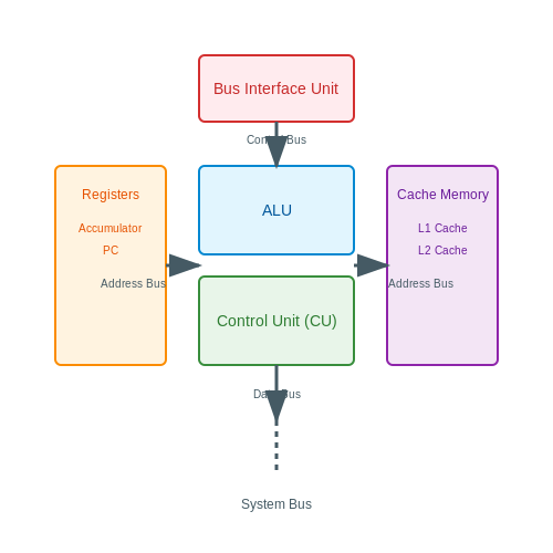
The microprocessor's architecture consists of several key components:
- Arithmetic Logic Unit (ALU) – Performs mathematical and logical operations (e.g., addition, AND/OR gates).
- Control Unit (CU) – Directs instruction flow by decoding and executing fetched instructions.
- Registers – Small, high-speed memory units (e.g., accumulator, program counter) for temporary data storage.
- Cache Memory – L1/L2 caches reduce latency by storing frequently accessed data.
- Bus Interface Unit – Manages data transfer between the CPU and external memory/peripherals via address, data, and control buses.
Instruction Execution Pipeline
Modern microprocessors use pipelining to enhance throughput. A typical 5-stage RISC pipeline includes:
- Fetch – Retrieves the next instruction from memory.
- Decode – Interprets the instruction and reads registers.
- Execute – The ALU performs the operation.
- Memory Access – Loads/stores data if required.
- Writeback – Updates registers with results.
Pipeline efficiency is governed by throughput (instructions/cycle) and latency. Hazards (structural, data, control) can stall the pipeline, mitigated via techniques like forwarding and branch prediction.
Clock Speed and Power Dissipation
The clock frequency (f) determines the rate of instruction execution. Dynamic power consumption follows:
where C is capacitance, and V is supply voltage. Modern designs balance performance and thermal constraints using dynamic voltage/frequency scaling (DVFS).
Real-World Implementation
In x86-64 architectures (e.g., Intel Core, AMD Ryzen), superscalar execution and out-of-order processing further optimize performance. Embedded systems (e.g., ARM Cortex-M) prioritize power efficiency with simpler pipelines.
1.2 Evolution of Microprocessor Technology
Early Developments (1970s)
The first commercially available microprocessor, the Intel 4004, emerged in 1971 as a 4-bit processor with a clock speed of 740 kHz and a transistor count of 2,300. Designed for calculators, it demonstrated the feasibility of integrating a central processing unit (CPU) onto a single chip. The MOS Technology 6502 (1975) and Zilog Z80 (1976) followed, introducing 8-bit architectures that enabled early personal computers like the Apple I and Commodore PET.
16-bit and 32-bit Eras (1980s)
The transition to 16-bit processors, such as the Intel 8086 (1978), marked a significant leap in computational power, addressing up to 1 MB of memory. The Motorola 68000 (1979), though internally 32-bit, featured a 16-bit external bus and became the backbone of early workstations like the Apple Macintosh. By the mid-1980s, fully 32-bit architectures like the Intel 80386 (1985) introduced virtual memory support and multitasking capabilities.
Performance Scaling and Moore’s Law (1990s–2000s)
The 1990s saw exponential growth in transistor counts, driven by advancements in CMOS technology. The Intel Pentium (1993) introduced superscalar architecture, enabling multiple instructions per clock cycle. By the 2000s, clock speeds surpassed 3 GHz, but thermal limitations led to a shift toward multi-core designs, exemplified by the Intel Core 2 Duo (2006). Moore’s Law—the observation that transistor counts double every two years—began facing physical limits as feature sizes approached atomic scales.
Modern Architectures (2010s–Present)
Contemporary processors leverage heterogeneous computing, combining general-purpose cores (CPU) with specialized units like GPUs (e.g., AMD Ryzen) and AI accelerators (e.g., Apple M1). FinFET transistors and extreme ultraviolet (EUV) lithography enable 5 nm and smaller process nodes. Quantum effects, such as tunneling, now dominate leakage currents, prompting research into post-silicon materials like gallium nitride (GaN) and carbon nanotubes.
Key Milestones
- 1971: Intel 4004 (4-bit, 2.3k transistors)
- 1978: Intel 8086 (16-bit, x86 ISA)
- 1985: Intel 80386 (32-bit, pipelining)
- 2006: Intel Core 2 Duo (multi-core)
- 2020: Apple M1 (ARM-based, 5 nm)
Technological Challenges
Power density and heat dissipation now limit clock frequency scaling. Dark silicon—regions of a chip that must remain inactive to avoid overheating—has become a critical design constraint. Solutions include:
where P is power, C is capacitance, V is voltage, and f is frequency. Reducing V via lower process nodes (e.g., 3 nm) remains a primary focus.
Basic Architecture and Functional Units
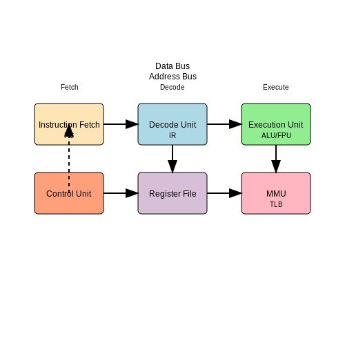
The fundamental architecture of a microprocessor consists of several key functional units that work in concert to execute instructions. At its core, the von Neumann architecture remains the dominant paradigm, though modern implementations incorporate numerous optimizations.
Instruction Fetch Unit
The instruction fetch unit retrieves program instructions from memory. It consists of:
- Program Counter (PC) - Holds the memory address of the next instruction
- Instruction Register (IR) - Stores the currently executing instruction
- Prefetch Buffer - Temporarily holds upcoming instructions to mitigate memory latency
Modern processors employ sophisticated branch prediction algorithms to minimize pipeline stalls during instruction fetch. The fetch unit typically interfaces with a dedicated instruction cache (L1i) for improved performance.
Decode Unit
The decode unit interprets fetched instructions and generates control signals. Key components include:
- Instruction Decoder - Translates opcodes into micro-operations
- Register Alias Table - Manages register renaming for out-of-order execution
- Microcode ROM - Stores complex instruction sequences (in CISC architectures)
Modern decode units often implement a queue-based design to handle variable-length instructions and parallel decoding. The decode throughput directly impacts the processor's overall instructions-per-cycle (IPC) metric.
Execution Unit
The execution unit performs arithmetic and logical operations. It contains:
- Arithmetic Logic Unit (ALU) - Handles integer operations
- Floating-Point Unit (FPU) - Manages floating-point calculations
- Vector Processing Unit - Accelerates SIMD operations (e.g., AVX, NEON)
Execution units implement pipelining to improve throughput. A typical RISC pipeline might consist of:
where CPI represents cycles per instruction. Modern processors achieve CPI < 1 through superscalar execution and speculative execution techniques.
Memory Management Unit (MMU)
The MMU handles memory access and address translation through:
- Translation Lookaside Buffer (TLB) - Caches virtual-to-physical address mappings
- Page Table Walker - Handles TLB misses
- Load-Store Queue - Manages memory access ordering
The MMU implements privilege levels and memory protection mechanisms critical for modern operating systems. Address translation follows:
Register File
The register file provides fast operand storage with typical characteristics:
- General-Purpose Registers - 16-32 registers in modern architectures
- Special-Purpose Registers - Flags, stack pointers, program counters
- Register Renaming - Enables out-of-order execution
Register access time follows:
where each term represents a stage in the register file's physical implementation.
Control Unit
The control unit orchestrates pipeline execution through:
- Pipeline Scheduling - Manages instruction flow and hazard resolution
- Branch Prediction - Reduces control hazards (modern predictors achieve >95% accuracy)
- Power Management - Implements clock gating and dynamic voltage/frequency scaling
Control logic complexity scales with pipeline depth and superscalar width. Modern processors employ distributed control with finite state machines managing each pipeline stage.
Interconnect Architecture
On-chip communication occurs through:
- Data Buses - Carry operands between functional units
- Control Lines - Transmit timing and coordination signals
- Network-on-Chip (NoC) - Scalable interconnect for many-core designs
Interconnect delay dominates in deep submicron processes, with propagation time following:
where Rint and Cint represent interconnect resistance and capacitance, L is wire length, and vprop is signal propagation velocity.
2. Instruction Set Architecture (ISA)
2.1 Instruction Set Architecture (ISA)
Definition and Core Components
The Instruction Set Architecture (ISA) defines the interface between software and hardware in a microprocessor, specifying the set of instructions that the processor can execute. It includes:
- Instruction formats — Binary encoding of operations and operands.
- Registers — Storage locations directly accessible to the processor.
- Addressing modes — Methods for specifying operand locations (e.g., immediate, register-indirect).
- Memory model — Byte-addressability, alignment constraints, and endianness.
- Control flow operations — Branches, jumps, and subroutine calls.
Classification of ISAs
ISAs are broadly categorized by their design philosophy:
- Reduced Instruction Set Computing (RISC) — Fixed-length instructions, load-store architecture, and a limited set of orthogonal operations (e.g., ARM, RISC-V).
- Complex Instruction Set Computing (CISC) — Variable-length instructions, memory-to-memory operations, and specialized instructions (e.g., x86).
- Very Long Instruction Word (VLIW) — Explicit parallelism encoded in instruction bundles (e.g., Intel Itanium).
Mathematical Modeling of Instruction Execution
The execution time of an instruction can be modeled as:
where \( N_{\text{cycles}} \) depends on the pipeline depth and hazards (structural, data, control). For a superscalar processor with issue width \( w \):
where \( P(\text{issue}_i) \) is the probability of issuing \( i \) instructions per cycle.
Practical Considerations
Modern ISAs incorporate features to optimize performance and power:
- SIMD extensions (e.g., AVX, NEON) for data-level parallelism.
- Predicated execution to reduce branch penalties.
- Variable-length encoding (e.g., x86-64) for code density.
Case Study: RISC-V vs. x86
RISC-V's modular ISA allows custom extensions (e.g., floating-point, vector operations), while x86 maintains backward compatibility at the cost of decoder complexity. The x86 μop cache mitigates decode overhead by caching decoded instructions.
2.2 Registers and Data Paths
Register Architecture
Registers are the fastest accessible storage locations within a microprocessor, implemented using flip-flops or static RAM cells. Their primary function is to hold operands, addresses, or intermediate results during computation. In modern processors, registers are classified into:
- General-Purpose Registers (GPRs): Used for arithmetic, logic, and data movement operations.
- Special-Purpose Registers: Include the Program Counter (PC), Stack Pointer (SP), and Status Register (Flags).
- Vector/SIMD Registers: Support single-instruction multiple-data (SIMD) operations for parallel processing.
Data Path Organization
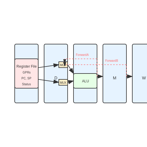
The data path defines the flow of data between registers, the Arithmetic Logic Unit (ALU), and memory. A typical RISC processor data path consists of:
- Register File: A bank of GPRs with multiple read/write ports for simultaneous access.
- ALU: Performs arithmetic and logical operations on register operands.
- Multiplexers (MUXes): Select between register outputs, immediate values, or memory data.
- Pipeline Stages: Segmented into Fetch, Decode, Execute, Memory, and Writeback (FDEMW) stages.
Register File Timing Constraints
The register file must satisfy setup and hold time requirements to ensure correct operation. The minimum clock period Tclk is constrained by:
where Tprop is the propagation delay through combinational logic, Tsetup is the register setup time, and Twire accounts for interconnect delays.
Bypassing and Hazard Mitigation
Data hazards occur when an instruction depends on the result of a preceding instruction still in the pipeline. Modern processors employ forwarding/bypassing to route ALU outputs directly to dependent instructions, avoiding pipeline stalls. The forwarding logic can be expressed as:
This condition checks if the ALU result from the Execute stage should bypass the register file for the next instruction's source operand.
Case Study: ARM Cortex-M Data Path
The ARM Cortex-M series employs a 3-stage pipeline (Fetch-Decode-Execute) with a unified register file (R0-R15). Key optimizations include:
- Zero Latency Branching: Pre-fetches branch targets during Decode stage.
- Single-Cycle Multiplier: Integrated in the data path for fast multiply operations.
- Memory-Mapped Registers: Special registers like CONTROL and PRIMASK are accessible via load/store instructions.
2.3 Pipelining and Parallel Processing
Instruction Pipelining
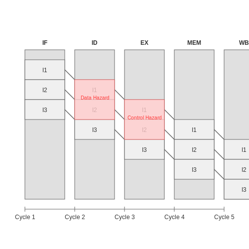
Pipelining divides the execution of a single instruction into multiple stages, allowing concurrent processing of multiple instructions. A typical RISC pipeline consists of five stages:
- Instruction Fetch (IF): Retrieves the next instruction from memory.
- Instruction Decode (ID): Decodes the instruction and reads register values.
- Execute (EX): Performs arithmetic or logic operations.
- Memory Access (MEM): Reads/writes data memory if required.
- Write Back (WB): Updates the register file with results.
For an n-stage pipeline with k instructions, the ideal speedup is given by:
In practice, hazards such as data dependencies, structural conflicts, and branch mispredictions reduce efficiency.
Parallel Processing Architectures
Parallelism is achieved through multiple execution units or cores. Key architectures include:
- Superscalar: Executes multiple instructions per cycle by dispatching them to redundant functional units.
- VLIW (Very Long Instruction Word): Bundles independent operations into a single wide instruction, relying on compiler scheduling.
- Multicore: Integrates multiple CPU cores on a single die, enabling thread-level parallelism.
Amdahl's Law quantifies the theoretical speedup from parallelization:
where P is the parallelizable fraction and N is the number of processors.
Out-of-Order Execution
Modern processors dynamically reorder instructions to avoid stalls. A Tomasulo algorithm-based scheduler uses reservation stations and register renaming to resolve dependencies. The reorder buffer (ROB) ensures sequential commit despite out-of-order execution.
Case Study: Intel Hyper-Threading
Hyper-Threading duplicates architectural states (e.g., registers) while sharing execution units, allowing two threads to run concurrently on a single core. This improves utilization but can lead to resource contention.
SIMD and Vector Processing
Single Instruction, Multiple Data (SIMD) units (e.g., AVX, NEON) perform identical operations on multiple data elements simultaneously. For a vector of length L, the theoretical throughput gain is:
Applications include image processing, scientific computing, and machine learning.
3. Fetch-Decode-Execute Cycle
3.1 Fetch-Decode-Execute Cycle
The Fetch-Decode-Execute (FDE) cycle is the fundamental operational mechanism of a microprocessor, dictating how instructions are processed sequentially. This cycle consists of three primary phases: fetching an instruction from memory, decoding it into actionable signals, and executing the operation. The efficiency of this cycle directly impacts processor performance, making it a critical area for optimization in modern architectures.
Instruction Fetch Phase
During the fetch phase, the microprocessor retrieves the next instruction from memory. The Program Counter (PC) holds the memory address of the current instruction and increments automatically after each fetch. The memory fetch operation can be modeled as:
where Memory[PC] denotes the data stored at the address specified by the PC. The fetched instruction is then stored in the Instruction Register (IR). In pipelined architectures, the fetch unit operates concurrently with other stages to maximize throughput.
Instruction Decode Phase
The decode phase interprets the fetched instruction. The Control Unit (CU) breaks down the opcode and operands, generating control signals that configure the processor's datapath. For example, an arithmetic instruction like ADD R1, R2 would:
- Identify the opcode (ADD) and source registers (R1, R2).
- Activate the ALU for addition.
- Route register values to the ALU inputs.
Modern processors use microcode or hardwired control for decoding, with trade-offs between flexibility and speed.
Execution Phase
The execute phase carries out the decoded operation. Depending on the instruction, this may involve:
- Arithmetic/Logic Operations: The ALU performs computations (e.g., ADD, SUB, AND).
- Memory Access: Load/store operations interact with data memory.
- Control Flow: Branches and jumps modify the PC to alter instruction sequence.
For example, executing MOV [R1], R2 would:
- Compute the effective address from R1.
- Write the value of R2 to the computed memory location.
- Update status flags if applicable.
Timing and Pipelining
The FDE cycle's duration is governed by the processor's clock speed. A single-cycle implementation completes all phases in one clock period, while pipelined processors overlap stages for higher throughput. The ideal speedup for an n-stage pipeline is:
where T represents execution time. Real-world pipelines face hazards (structural, data, control) that reduce efficiency.
Real-World Considerations
Modern processors enhance the basic FDE cycle with:
- Superscalar Execution: Multiple instructions fetched/executed per cycle.
- Out-of-Order Execution: Dynamically reorders instructions to minimize stalls.
- Speculative Execution: Predicts branches to prefetch instructions.
For instance, Intel's x86 architectures employ a decoupled front-end/back-end design, where the fetch/decode units feed a reorder buffer that schedules instructions for execution units.
3.2 Interrupt Handling and Exceptions
Interrupt Types and Sources
Microprocessors handle interrupts as asynchronous signals that temporarily suspend normal program execution to service higher-priority events. Interrupts are broadly classified into:
- Hardware Interrupts — Triggered by external devices (e.g., timers, I/O peripherals) via dedicated pins like INT or NMI.
- Software Interrupts — Generated by instructions (e.g., INT n in x86, SWI in ARM) for system calls or debugging.
- Exceptions — Synchronous events from erroneous execution (e.g., division by zero, page faults).
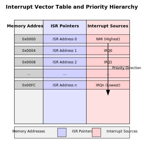
Interrupt Vector Table (IVT) and Priority
The IVT maps interrupt requests (IRQs) to memory addresses of corresponding Interrupt Service Routines (ISRs). Priority is resolved via:
Modern architectures like ARM Cortex-M use a Nested Vectored Interrupt Controller (NVIC) for dynamic prioritization.
Interrupt Latency and Context Switching
Latency is the delay between interrupt assertion and ISR execution, calculated as:
Critical sections disable interrupts via CLI (x86) or __disable_irq() (ARM) to prevent race conditions.
Exception Handling in Pipelined Architectures
Exceptions in superscalar processors require precise handling to ensure all prior instructions complete before the ISR runs. The Program Counter (PC) is saved to the stack or a dedicated register (e.g., LR in ARM).
Real-World Implementation: x86 vs. ARM
- x86 — Uses an IVT in real mode or an Interrupt Descriptor Table (IDT) in protected mode. The iret instruction restores context.
- ARM — Employs banked registers (R13–R14) for fast context switching. Exceptions trigger mode transitions (e.g., IRQ mode).
Debugging and Performance Tradeoffs
Excessive interrupts can degrade throughput. Profiling tools (e.g., perf on Linux) measure ISR duration and jitter. Techniques like interrupt coalescing mitigate overhead in high-throughput systems.
3.3 Memory Access and Management
Memory Hierarchy and Access Latency
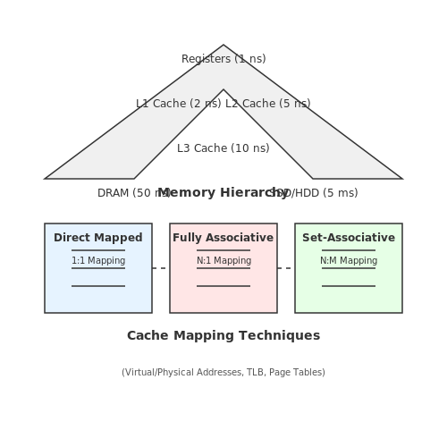
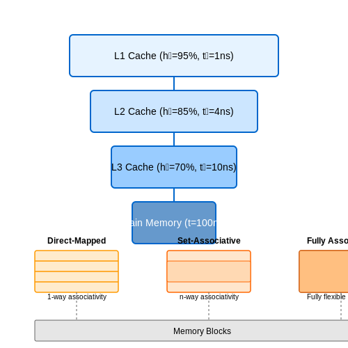
Modern microprocessors employ a hierarchical memory structure to balance speed, cost, and capacity. The hierarchy typically includes registers, cache (L1, L2, L3), main memory (DRAM), and secondary storage (SSD/HDD). Access latency increases exponentially as we move down the hierarchy. For instance, L1 cache access times are in the order of nanoseconds, while DRAM accesses take tens to hundreds of nanoseconds. This latency is modeled by:
where hL1 and hL2 are hit rates for L1 and L2 caches, respectively, and tL1, tL2, tDRAM are their respective access times.
Address Translation and Virtual Memory
Virtual memory allows programs to operate as if they have contiguous memory, while physical memory may be fragmented. The Memory Management Unit (MMU) translates virtual addresses to physical addresses using page tables. A typical translation involves:
Translation Lookaside Buffers (TLBs) cache recent translations to reduce lookup overhead. A TLB miss triggers a page table walk, which may require multiple memory accesses.
Cache Organization and Mapping Techniques
Caches are organized into sets and lines to optimize spatial and temporal locality. Three primary mapping techniques are used:
- Direct-Mapped: Each memory block maps to exactly one cache line.
- Fully Associative: A block can reside in any cache line.
- Set-Associative: A compromise where blocks map to a set of lines (e.g., 4-way set-associative).
The cache hit rate depends on the replacement policy (LRU, FIFO, Random) and the degree of associativity.
Memory Consistency Models
In multi-core systems, memory consistency defines the order in which writes become visible to other processors. The most common models include:
- Sequential Consistency: All memory operations appear to execute in program order.
- Weak Consistency: Allows reordering but requires explicit synchronization.
- Release Consistency: Further relaxes ordering constraints between synchronization points.
Modern processors often implement Total Store Order (TSO), a relaxed variant of sequential consistency.
Memory Bandwidth and Prefetching
Bandwidth limitations arise when multiple cores contend for shared memory. Techniques like prefetching mitigate this by predicting future accesses and loading data into cache ahead of time. Hardware prefetchers analyze stride patterns, while software prefetching relies on compiler hints (e.g., __builtin_prefetch in GCC).
Real-World Implications
In high-performance computing, inefficient memory access patterns can bottleneck performance. For example, false sharing occurs when unrelated variables share a cache line, leading to unnecessary invalidations. Optimizing data layout (e.g., padding, alignment) can significantly improve throughput.
4. Clock Speed and Instruction Throughput
4.1 Clock Speed and Instruction Throughput
Fundamentals of Clock Speed
The clock speed of a microprocessor, measured in Hertz (Hz), defines the rate at which the processor's clock generator oscillates. A single clock cycle represents the smallest discrete time unit in which synchronous logic operations occur. For a processor running at 3 GHz, the clock period T is:
This period constrains the execution time of pipeline stages, memory access, and combinatorial logic paths. Modern processors use phase-locked loops (PLLs) to multiply a base clock signal, enabling higher frequencies while maintaining synchronization with external components.
Instruction Throughput and CPI
Throughput, measured in instructions per second (IPS), depends on both clock speed and the average cycles per instruction (CPI). For an n-stage pipeline, ideal CPI is 1, but hazards (structural, data, or control) increase it. The theoretical throughput is:
For example, a 5 GHz processor with CPI=1.2 achieves 4.17 billion IPS. Superscalar architectures further improve throughput by issuing multiple instructions per cycle (IPC), with modern designs reaching IPC > 6 via out-of-order execution and speculative branching.
Clock Speed vs. Performance Scaling
While higher clock speeds reduce instruction latency, performance scales nonlinearly due to:
- Power dissipation: Dynamic power Pd grows with fV2, limiting practical frequencies.
- Memory bottlenecks: DRAM access times (~50 ns) often stall high-frequency CPUs.
- Instruction-level parallelism (ILP): Diminishing returns occur when dependencies exceed available execution units.
Case Study: Overclocking Trade-offs
Overclocking a CPU from 4.0 GHz to 5.0 GHz (25% increase) may yield only 15% higher throughput due to increased cache misses and thermal throttling. The Amdahl’s Law limit applies:
where p is the parallelizable fraction and s is the clock speedup factor. For p=0.8 and s=1.25, speedup caps at 1.19×.
Advanced Techniques for Throughput Optimization
Modern designs mitigate clock speed limitations via:
- Dynamic frequency scaling (e.g., Intel Turbo Boost), adjusting f based on workload.
- Simultaneous multithreading (SMT), masking latency by interleaving threads.
- Branch prediction, reducing control hazards to maintain CPI ≈1.
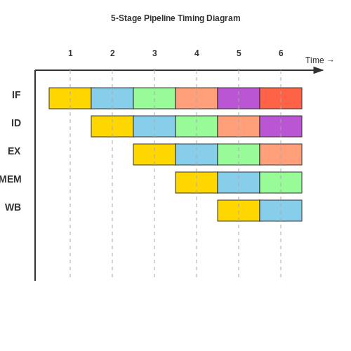
The diagram illustrates a 5-stage pipeline (IF=Instruction Fetch, ID=Decode, EX=Execute, MEM=Memory, WB=Write Back). At CPI=1, one instruction completes per cycle after an initial latency of 5 cycles.
4.2 Cache Memory and Performance Impact
Cache Hierarchy and Latency Reduction
Modern microprocessors employ a multi-level cache hierarchy (L1, L2, L3) to bridge the growing speed gap between CPU cores and main memory. The access latency increases exponentially with each cache level due to physical constraints, while the hit rate improves with larger cache sizes. The effective memory access time (teff) can be modeled as:
where hn and tn represent the hit rate and access time for cache level n, respectively. This nonlinear relationship explains why even small improvements in L1 hit rates yield disproportionate performance gains.
Cache Mapping Techniques
Three primary mapping strategies govern cache organization:
- Direct-mapped: Simplest implementation where each memory block maps to exactly one cache line, causing collisions.
- Set-associative: Compromise between flexibility and complexity, with n-way associativity allowing blocks to occupy any of n lines.
- Fully associative: Maximum flexibility (any block in any line) at the cost of complex parallel search logic.
The miss penalty for an n-way set-associative cache follows:
where C is cache size, B is block size, S is associativity, and k is a program-dependent constant (typically 0.3–0.7).
Prefetching and Spatial Locality
Modern processors employ stream buffers and stride prediction to exploit spatial locality. The prefetch accuracy (A) directly impacts performance gains:
where CPI is cycles per instruction and I is instruction count. ARM's Cortex-A78 demonstrates this with its machine-learning prefetcher achieving 85% accuracy for stride patterns.
Coherency Protocols in Multicore Systems
The MESI protocol (Modified, Exclusive, Shared, Invalid) maintains consistency across cores through state transitions that incur latency penalties. The probability of cache-to-cache transfers (Pct) in an N-core system scales as:
This explains why AMD's Zen 3 architecture implements a unified L3 cache with victim replication to reduce cross-core snooping.
Real-World Performance Case Study
Intel's Sunny Cove microarchitecture demonstrates cache optimizations through:
- Non-inclusive L3 cache reducing duplication (8% area savings)
- Write-back bandwidth increased to 64 bytes/cycle
- Load/store buffers enlarged by 50% to hide L1 miss latency
These changes yield a 12–18% IPC improvement in SPECint2017 benchmarks compared to Skylake, with 40% of gains attributed to cache subsystem enhancements.
4.3 Power Consumption and Heat Dissipation
Fundamentals of Power Dissipation in Microprocessors
Power consumption in microprocessors arises primarily from dynamic switching losses and static leakage currents. The total power dissipation Ptotal can be expressed as:
Dynamic power (Pdynamic) is dominated by the charging and discharging of capacitive loads during transistor switching:
where α is the activity factor, C is the load capacitance, V is the supply voltage, and f is the clock frequency. Static power (Pstatic) results from subthreshold leakage and gate leakage, modeled as:
Thermal Resistance and Heat Dissipation
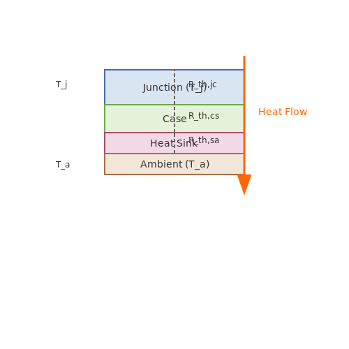
The heat generated must be dissipated to prevent thermal runaway. The junction temperature Tj is governed by:
where Ta is the ambient temperature and Rth is the thermal resistance between the junction and ambient. For multi-layer systems (e.g., die + heat sink), total thermal resistance sums in series:
Rth,jc (junction-to-case), Rth,cs (case-to-sink), and Rth,sa (sink-to-ambient) are critical for thermal design.
Advanced Cooling Techniques
Phase-change cooling and thermoelectric coolers (TECs) are used in high-performance systems. The effectiveness of a TEC is quantified by its coefficient of performance (COP):
where Qc is the heat pumped and Pinput is the electrical power consumed. For liquid cooling, the heat transfer rate Q is:
with ṁ as the mass flow rate, cp as the specific heat, and ΔT as the temperature difference.
Real-World Design Trade-offs
In modern processors, Dynamic Voltage and Frequency Scaling (DVFS) reduces power by quadratically lowering V at the cost of linear performance loss. For example, a 20% voltage reduction yields a 36% power saving. However, leakage current increases exponentially with temperature, necessitating careful thermal management.
Finite Element Analysis (FEA) simulations are routinely employed to model heat distribution in 3D processor layouts, optimizing heat sink geometry and material selection (e.g., copper vs. vapor chambers).
5. Embedded Systems and IoT
5.1 Embedded Systems and IoT
Architecture of Embedded Systems
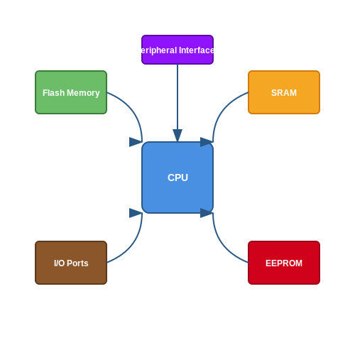
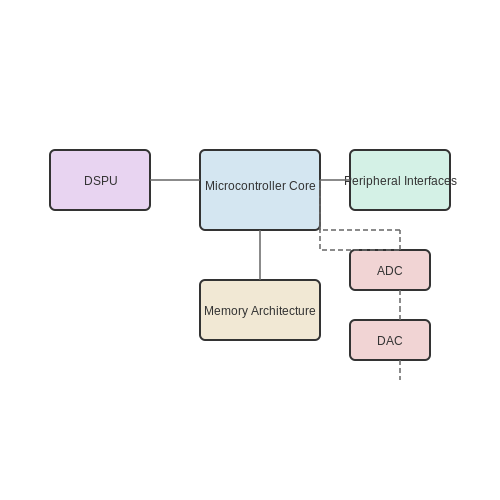
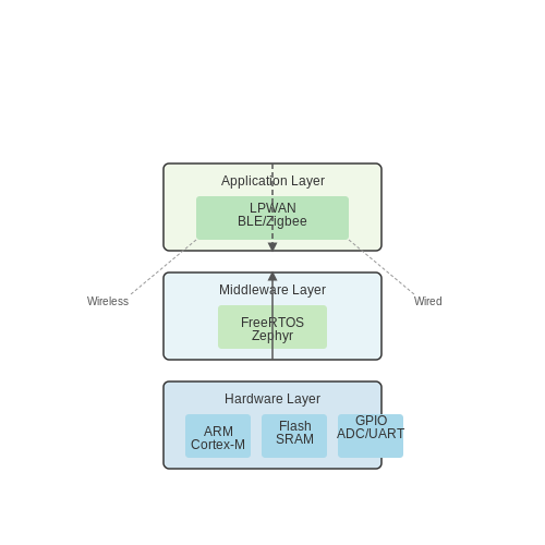
Embedded systems integrate microprocessors or microcontrollers with dedicated peripherals to perform specific tasks. Unlike general-purpose computing systems, they are optimized for real-time operation, low power consumption, and deterministic behavior. A typical embedded system consists of:
- Processor Core: ARM Cortex-M, RISC-V, or x86-based architectures.
- Memory Hierarchy: Flash for firmware, SRAM for runtime data, and sometimes external DRAM.
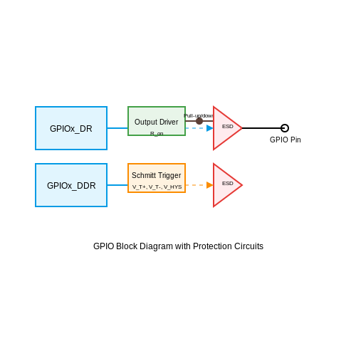
- Peripherals: GPIO, ADCs, DACs, UART, SPI, I²C, and timers.
- Real-Time Operating System (RTOS): FreeRTOS, Zephyr, or ThreadX for task scheduling.
Mathematical Modeling of Real-Time Constraints
For hard real-time systems, worst-case execution time (WCET) must satisfy:
where \( C_i \) is the execution time of task \( i \), \( T_i \) is its period, and \( U_{lub} \) is the least upper bound schedulability limit (e.g., 0.693 for Rate-Monotonic Scheduling).
IoT Communication Protocols
IoT extends embedded systems with networked connectivity. Key protocols include:
- LPWAN: LoRaWAN, NB-IoT for long-range, low-power communication.
- Short-Range: BLE 5.2, Zigbee 3.0, and Thread for mesh networks.
- IP-Based: MQTT-SN, CoAP over UDP for constrained devices.
Energy consumption for wireless transmission follows:
where \( P_{tx} \) is transmit power, \( t_{on} \) is active time, and \( E_{sw} \) is switching energy per packet.
Case Study: Edge AI in Embedded Systems
Modern embedded processors (e.g., NVIDIA Jetson, Coral TPU) deploy machine learning at the edge. A convolutional neural network (CNN) inference on a Cortex-M7 microcontroller involves:
- Quantization: 8-bit fixed-point arithmetic to reduce memory footprint.
- Hardware Acceleration: CMSIS-NN library for ARM SIMD instructions.
Latency for a single-layer CNN is approximated by:
where \( N_{ops} \) is operation count, \( f_{CLK} \) is clock frequency, and \( CPI \) is cycles per instruction.
Security Challenges in IoT
Embedded IoT devices face threats like side-channel attacks and firmware exploits. Countermeasures include:
- Secure Boot: Cryptographic verification of firmware integrity.
- Trusted Execution Environments (TEE): ARM TrustZone for isolated secure processing.
- Post-Quantum Cryptography: Lattice-based algorithms for future-proofing.
5.2 Multi-Core and Heterogeneous Processors
Architectural Foundations
Multi-core processors integrate multiple independent execution units (cores) on a single die, enabling parallel task execution. Unlike single-core designs, where performance scaling relies on increasing clock speeds, multi-core architectures distribute workloads across cores, mitigating thermal and power constraints. The theoretical speedup for N cores executing perfectly parallelizable code is given by Amdahl's Law:
where P is the parallelizable fraction of the workload. In practice, overhead from synchronization and memory contention reduces achievable gains.
Homogeneous vs. Heterogeneous Designs
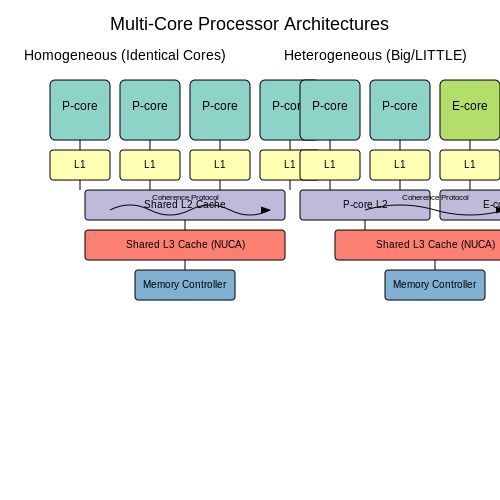
Homogeneous multi-core processors (e.g., Intel Xeon, AMD EPYC) employ identical cores, simplifying load balancing but limiting specialization. Heterogeneous processors (e.g., ARM big.LITTLE, NVIDIA Tegra) combine cores with differing performance/power characteristics, often pairing high-performance cores with energy-efficient ones. The scheduling policy for heterogeneous systems must account for:
- Core asymmetry in IPC (Instructions Per Cycle) and power profiles
- Thread migration latency between core types
- Cache coherence across dissimilar memory hierarchies
Cache Coherence Protocols
Multi-core systems require cache coherence to maintain data consistency. The MESI protocol (Modified, Exclusive, Shared, Invalid) is widely implemented, with each cache line existing in one of four states. For an N-core system, the coherence overhead scales as:
Directory-based protocols reduce broadcast traffic but introduce lookup latency. In heterogeneous systems, non-uniform cache architectures (NUCA) further complicate coherence due to divergent access times.
Real-World Implementations
ARM DynamIQ
ARM's DynamIQ microarchitecture allows mixing Cortex-A7x and Cortex-A5x cores in a single cluster with shared L3 cache. The QoS-aware memory controller prioritizes latency-sensitive tasks on big cores while throttling LITTLE cores during memory bottlenecks.
Intel Hybrid Architecture
Intel's 12th-gen Alder Lake combines Golden Cove (P-cores) and Gracemont (E-cores) with a Thread Director hardware scheduler. The P-cores support hyperthreading and wider out-of-order execution, while E-cores optimize for throughput-per-watt in background tasks.
Performance Modeling
The roofline model characterizes heterogeneous processor performance by plotting attainable FLOPs against operational intensity (OI):
where π is peak compute throughput and σ is memory bandwidth. Heterogeneous systems exhibit multiple rooflines corresponding to each core type, requiring workload partitioning that maximizes proximity to the optimal roofline.
Emerging Trends
Recent research focuses on chiplets (discrete dies interconnected via high-bandwidth links) and 3D stacking to overcome reticle limits. AMD's EPYC processors demonstrate chiplet scalability, while Intel's Foveros technology stacks compute dies atop memory/interconnect layers, achieving 1 TB/s/mm² inter-layer bandwidth.
5.3 AI and Machine Learning Accelerators
Architectural Specialization for Neural Networks
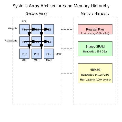
Modern AI accelerators leverage dataflow architectures optimized for matrix operations, contrasting with von Neumann processors. The systolic array design, pioneered by H.T. Kung in 1982, enables parallel multiply-accumulate (MAC) operations by propagating partial results through a grid of processing elements (PEs). For an N×N systolic array performing matrix multiplication C = AB, each PE computes:
This architecture eliminates memory bottlenecks by streaming weights and activations directly between PEs, achieving 90%+ utilization rates compared to <30% in GPUs.
Precision-Adaptive Compute Units
AI accelerators employ mixed-precision arithmetic to balance computational efficiency with model accuracy. Tensor cores in NVIDIA's Ampere architecture, for instance, support:
- FP64: 2.5 TFLOPS (scientific computing)
- TF32: 20 TFLOPS (training)
- INT8: 160 TOPS (inference)
The energy savings follow the quadratic relationship:
where n is the bit-width, making INT8 operations ~64× more energy-efficient than FP32.
Sparsity Exploitation
Advanced accelerators like Google's TPUv4 implement structured sparsity by pruning weights below a threshold θ during training. For a layer with sparsity ratio s, the effective computation reduces to:
With s=0.9 (90% zeros), this yields 10× theoretical speedup while maintaining <1% accuracy loss in ResNet-50 models.
On-Chip Memory Hierarchy
AI accelerators implement a software-managed scratchpad memory system to overcome DRAM bandwidth limitations. The memory hierarchy typically includes:
- Register files (1-10 cycles latency, 10TB/s bandwidth)
- Shared SRAM (10-100 cycles, 1TB/s)
- HBM2/3 (100-300 cycles, 500GB/s)
The optimal tile size T for matrix multiplication follows:
where Mcache is the available SRAM capacity.
Case Study: NVIDIA Hopper Architecture
The GH100 chip demonstrates state-of-the-art design with:
- 132 SM (Streaming Multiprocessor) clusters
- 576 Tensor cores (4× faster FP16 than Ampere)
- 3TB/s NVLink interconnect
For transformer models, Hopper achieves 6× higher throughput than previous generations through transformer engine optimizations that dynamically switch between FP8 and FP16 precision.
6. Key Textbooks and Research Papers
6.1 Key Textbooks and Research Papers
- MIT OpenCourseWare | Electrical Engineering and Computer Science | 6.01 ... — Description 6.01 explores fundamental ideas in electrical engineering and computer science, in the context of working with mobile robots. Key engineering principles, such as abstraction and modularity, are applied in the design of computer programs, electronic circuits, discrete-time controllers, and noisy and/or uncertain systems.
- The X86 Microprocessors: Architecture and Programming (8086 to Pentium ... — She has presented research papers in conferences of national andinternational stature and has worked on numerous projects based on microprocessors and microcontrollers, such as microprocessor-based voting machines and microcontroller-based rail track switching system.
- Lyla B. Das, The x86 Microprocessors: 8086 to Pentium, Multicores, Atom ... — She has presented research papers in conferences of national and international stature and has worked on numerous projects based on microprocessors and microcontrollers.
- (PDF) Fundamentals of Electronic Systems Design - Academia.edu — It is the result of the extensive experience of its two authors in industry, academic research, and teaching in electronic systems design. Its aim is to support the reader with the development and fabrication of modern electronic devices, taking all relevant aspects into consideration with a clear presentation of the underlying technical and ...
- PDF AM-(ch-01) - Clark Science Center — 1.1 GENERAL A microprocessor is one of the most exciting technological innovations in electronics since the appearance of the transistor in 1948. This wonder device has not only set in the process of revolutionizing the field of digital electronics, but it is also getting entry into almost every sphere of human life. Applications of microprocessors range from the very sophisticated process ...
- PDF Microprocessor Architecture — The policies and mechanisms needed for out-of-order processing, such as register renaming, reservation stations, and reorder buffers Optimizations for high performance, such as branch predictors, instruction scheduling, and load-store speculations Design choices and enhancements to tolerate latency in the cache hierarchy of single and multiple processors State-of-the-art multithreading and ...
- (PDF) 8086- microprocessor and interfacing and others - ResearchGate — The aim of the book is to deal with microprocessor, their interfacing, supporting chips, interfacing circuits and devices, peripherals etc. It includes assembly language programming of Intel 8085.
- Behrooz Parhami's Textbook on Computer Architecture — References to seminal papers in computer architecture, key design ideas, and important state-of-the-art research contributions are listed at the end of each chapter. These references provide good starting points for doing in-depth studies or for preparing term papers/projects.
- (PDF) History, Structure And Types Of Microprocessors — PDF | This article gives you a brief overview on microprocessor types, performance, and computer hardware. The article also provides basic concepts... | Find, read and cite all the research you ...
- Fundamentals of Layout Design for Electronic Circuits — Quality Electronic Design, …, 2002 In this paper, we describe a comprehensive layout methodology for bonded three-dimensional integrated circuits (3D ICs). In bonded 3D integration technology, parts of a circuit are fabricated on different wafers, and then, the wafers are bonded with a glue layer of Cu or polymer based adhesive.
6.2 Online Resources and Tutorials
- 6.2. Setup and Walk-through — ESE532 Handouts Fall 2021 — 6.2.2. Useful Resources Following the previous HW, we will create Vitis project using Vitis IDE. Note that Makefiles are automatically generated when we build the project in GUI mode, and you are welcome to use Makefiles later in the project. In fact, many of Vitis tutorials on the web are using Makefile, which we highly recommend you to browse around while you are doing this lab. In this HW ...
- EMK310 Study Guide 2022.pdf - Study Guide Department of... - Course Hero — Microprocessors' architectures, instruction sets and the interaction between microprocessors and the outside world are investigated to obtain a deeper knowledge of the functioning of these systems and how this knowledge is applicable to real engineering problems. 2 EDUCATIONAL APPROACH 2.1 General approach The teaching philosophy followed in ...
- 6.02 Intro to EECS 2 - Massachusetts Institute of Technology — An integrated, hands-on introduction to electrical engineering and computer science. Lectures and laboratory experiments explore modeling transmission systems in the time and frequency domains, analog and digital signaling, detecting and correcting errors, source coding, and the engineering of packet-switched networks. These explorations are used to illustrate some common EECS themes: the role ...
- Circuits and Electronics | Electrical Engineering and Computer Science ... — 6.002 is designed to serve as a first course in an undergraduate electrical engineering (EE), or electrical engineering and computer science (EECS) curriculum. At MIT, 6.002 is in the core of department subjects required for all undergraduates in EECS. The course introduces the fundamentals of the lumped circuit abstraction. Topics covered include: resistive elements and networks; independent ...
- Microprocessors EG573EX - ekendraonline.com — COURSE OBJECTIVES To introduce the operation, programming, and application of microprocessors.1.0 Introduction to Computer Architecture: (4 hours) 1.1 Automated calculator and stored program computer, Von Neuman, Harvard and modified Harvard architectures, principle elements - CPU, memory, control and input/output units 1.2 Simple stored program computer architecture, basic registers 1.3 ...
- PDF SEMESTER VI EEE - Rajagiri School of Engineering & Technology — PROGRAMME OUTCOMES Students will be able to apply the knowledge of mathematics, science, engineering fundamentals and Electrical and Electronics Engineering for solving complex engineering problems. Students will be able to design and conduct experiments, analyze and interpret data in the field of Electrical and Electronics Engineering.
- Microprocessor and Embedded System Design - Class Central — Dive into microprocessor architecture, embedded systems, and ARM CPU design, covering computer organization, memory systems, buses, and I/O interfaces with hands-on lab experience.
- Embedded Systems - Introduction to Microprocessors - MSP430 — Welcome to the "Introduction to Microprocessors-MSP430" course! This course is designed to provide students with a comprehensive understanding of microprocessor and microcontroller systems, with a focus on programming the MSP430 microcontroller.
- Lecture Notes | Microelectronic Devices and Circuits | Electrical ... — This section provides the schedule of lecture topics along with the lecture notes from each session.
- Introduction to EECS II: Digital Communication Systems | Electrical ... — An introduction to several fundamental ideas in electrical engineering and computer science, using digital communication systems as the vehicle. The three parts of the course—bits, signals, and packets—cover three corresponding layers of abstraction that form the basis of communication systems like the Internet. The course teaches ideas that are useful in other parts of EECS: abstraction ...
6.3 Industry Standards and Documentation
- CENELEC - EN 61000-6-3 - Electromagnetic compatibility (EMC) - Part 6-3 ... — Find the most up-to-date version of EN 61000-6-3 at GlobalSpec. ... Consumer Electronics Daily Digest Defense & Security Technology Electrical Components Electronic Components Electronic Design Solutions Electronic Test Equipment Electronics360 Factory ... Part 6-3: Generic standards - Emission standard for residential, commercial and light ...
- EN IEC 61000-6-3:2021 - iTeh Standards — EN IEC 61000-6-3:2021 - IEC 61000-6-3:2020 is a generic EMC emission standard applicable only if no relevant dedicated product or product family EMC emission standard has been published. This part of IEC 61000 for emission requirements applies to electrical and electronic equipment intended for use at residential (see 3.1.14) locations. This part of IEC 61000 also applies to electrical and
- IEC 61000-6-3 - Electromagnetic compatibility (EMC) - Part 6-3: Generic ... — IEC 61000-6-3:2020 is a generic EMC emission standard applicable only if no relevant dedicated product or product family EMC emission standard has been published. ... This part of IEC 61000 also applies to electrical and electronic equipment intended for use at other locations that do not fall within the scope of IEC 61000-6-8 or IEC 61000-6-4 ...
- IEC 61000-6-3 - Electromagnetic compatibility (EMC)- Part 6-3: Generic ... — Find the most up-to-date version of IEC 61000-6-3 at GlobalSpec. UNLIMITED FREE ACCESS TO THE WORLD'S BEST ... (EMC)- Part 6-3: Generic standards - Emission standard for equipment in residential environments ... This part of IEC 61000 also applies to electrical and electronic equipment intended for use at other locations that do not fall ...
- PDF Microprocessor Standards Committee of the IEEE Computer Society June 22 ... — Microprocessor Standards Committee Policies and Procedures for Standards Development 1.0 Introduction 1.0.1 Role of Standards Development and these Procedures In today's technological environment, standards play a critical role in product development and market competitiveness. In the IEEE, the responsibility for how a standard originates and
- PDF Edition 3.0 2020-07 INTERNATIONAL STANDARD NORME INTERNATIONALE — Part 6-3: Generic standards - Emission standard for equipment in residential environments . Compatibilité électromagnétique (CEM)- Partie 6-3: Normes génériques - Norme sur l'émission relative aux appareils utilisés dans les environnements résidentiels . IEC 61000-6-3 Edition 3.0 2020-07 INTERNATIONAL STANDARD NORME INTERNATIONALE IEC
- Iec 61000-6-3:2020 — IEC 61000-6-3:2020 is a generic EMC emission standard applicable only if no relevant dedicated product or product family EMC emission standard has been published. This part of IEC 61000 for emission requirements applies to electrical and electronic equipment intended for use at residential (see 3.1.14) locations. This part of IEC 61000 also ...
- Structuring of technical information and documentation - iTeh Standards — IEC 62023:2011 provides rules for applying a method of structuring technical information and documentation by using a main document (leading document) for the clustering of the information for each object. This second edition cancels and replaces the first edition of IEC 62023 published in 2000. This edition constitutes a technical revision. It includes the following substantial changes with ...
- PDF DESIGN ASSURANCE GUIDANCE FOR AIRBORNE ELECTRONIC HARDWARE - Archive.org — committee was chartered to develop clear and consistent design assurance guidance for electronic airborne hardware such that it safely performs its intended functions. Electronic airborne hardware includes line replaceable units, circuit board assemblies, application specific integrated circuits, programmable logic devices, etc.
- Specifications & Technologies - 3GPP — There are a variety of ways to find the right specification or to seek the meaning of a work plan acronym. This section will provide you with ways to get the spec. and how to find the technology areas covered by 3GPP.