Neuromorphic Engineering and Computing
1. Biological Inspiration: Neurons and Synapses
Biological Inspiration: Neurons and Synapses
The foundation of neuromorphic engineering lies in emulating the computational principles of biological neural systems. At the core of these systems are neurons and synapses, which exhibit remarkable efficiency in information processing compared to conventional digital architectures.
Neurons: Biological Signal Processors
Biological neurons are specialized cells that transmit electrochemical signals. Their behavior can be modeled mathematically using the Hodgkin-Huxley equations, which describe how action potentials are generated through ionic currents:
where Cm is the membrane capacitance, V is the membrane potential, and gNa, gK, gL represent conductance terms for sodium, potassium, and leakage channels respectively. The gating variables m, h, and n follow first-order kinetics.
For neuromorphic implementations, simplified models like the Leaky Integrate-and-Fire (LIF) neuron are often used:
When V reaches a threshold Vth, the neuron fires a spike and resets to Vreset. This abstraction captures essential neural dynamics while being computationally tractable for hardware implementation.
Synapses: Adaptive Weights
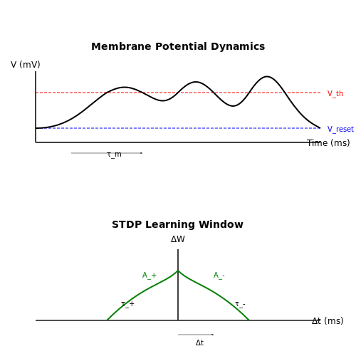
Synapses mediate communication between neurons and exhibit plasticity - the ability to modify their strength based on neural activity. The most studied plasticity mechanism is spike-timing-dependent plasticity (STDP), where synaptic weight changes depend on the precise timing of pre- and post-synaptic spikes:
Here, Δt = tpost - tpre is the spike timing difference, and A±, τ± determine the magnitude and time window of plasticity. This Hebbian learning rule enables unsupervised feature extraction in neuromorphic systems.
Neuromorphic Implementations
Modern neuromorphic chips implement these biological principles using mixed-signal circuits:
- Neuron circuits use capacitor-based integrators and comparator circuits to emulate membrane dynamics and spiking
- Synapse arrays employ non-volatile memory technologies (RRAM, PCM) or floating-gate transistors to store programmable weights
- Plasticity circuits implement STDP using differential pairs and time-to-voltage conversion
For example, IBM's TrueNorth chip implements 1 million programmable spiking neurons with 256 million configurable synapses, achieving 46 billion synaptic operations per second while consuming just 70mW - orders of magnitude more efficient than conventional processors for cognitive workloads.
Principles of Neuromorphic Computing
Biological Inspiration and Spiking Neural Networks
Neuromorphic computing draws direct inspiration from the biological brain's architecture and computational principles. Unlike traditional artificial neural networks (ANNs), which rely on continuous-valued activations, neuromorphic systems emulate spiking neural networks (SNNs), where information is encoded in the timing and frequency of discrete spikes. The leaky integrate-and-fire (LIF) model is a foundational mathematical representation of neuronal dynamics:
Here, \( \tau_m \) is the membrane time constant, \( V \) is the membrane potential, \( V_{rest} \) is the resting potential, \( R_m \) is the membrane resistance, and \( I_{syn}(t) \) represents synaptic input current. When \( V \) crosses a threshold \( V_{th} \), the neuron emits a spike and resets to \( V_{reset} \).
Event-Driven Computation
Neuromorphic systems exploit event-driven computation, where processing occurs only in response to spikes, drastically reducing energy consumption compared to clock-driven von Neumann architectures. This is formalized using asynchronous message passing, where synapses transmit spikes with precise temporal delays:
\( w_j \) denotes synaptic weights, \( t_j \) are spike times from presynaptic neuron \( j \), \( \Delta_{ij} \) is the axonal delay, and \( \alpha(\cdot) \) models the postsynaptic current kernel. This mirrors biological synaptic plasticity mechanisms like spike-timing-dependent plasticity (STDP):
Hardware Implementation
Neuromorphic hardware leverages mixed-signal circuits to emulate neuronal dynamics. Key components include:
- Silicon neurons: Analog circuits implementing LIF dynamics with subthreshold CMOS operation (e.g., transconductance amplifiers for \( \tau_m \)).
- Synaptic crossbars: Memristor arrays or SRAM-based weight storage enabling \( O(1) \) parallel multiply-accumulate (MAC) operations.
- Event routers: Asynchronous digital logic (e.g., address-event representation (AER)) for spike communication.
The energy efficiency is quantified by the synaptic operation (SynOp) metric, where state-of-the-art designs achieve < 1 pJ/SynOp, outperforming GPUs by 3–5 orders of magnitude for sparse spiking workloads.
Applications and Challenges
Neuromorphic computing excels in real-time edge applications:
- Robotics: Loihi and SpiNNaker chips enable millisecond-latency sensorimotor control.
- Neuromorphic sensing: Dynamic vision sensors (DVS) coupled with SNNs achieve < 10 mW power for object tracking.
Key challenges include nonlinear device variability (requiring calibration algorithms) and lack of standardized training frameworks for large-scale SNNs. Recent advances in surrogate gradient methods (e.g., sigmoidal spike gradient approximation) are bridging this gap.
1.3 Key Differences from Traditional Computing
Architectural Paradigm
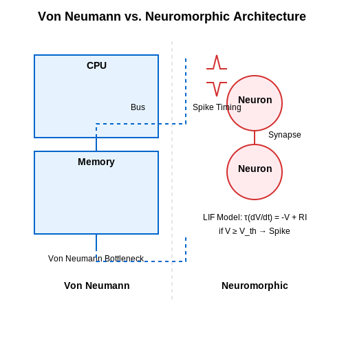
Traditional computing relies on the von Neumann architecture, where memory and processing units are physically separated, leading to the von Neumann bottleneck due to data transfer latency. Neuromorphic systems, in contrast, adopt a distributed, event-driven architecture inspired by biological neural networks. Here, computation and memory are co-located within synapses and neurons, eliminating the bottleneck and enabling massively parallel processing.
Information Representation
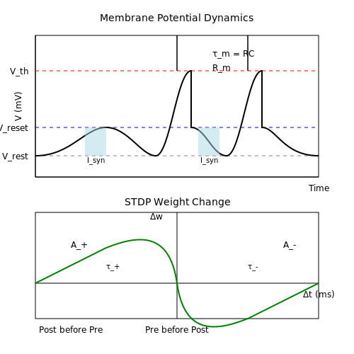
Conventional computers use deterministic, binary logic (0/1), whereas neuromorphic systems employ spikes (action potentials) as temporal, analog signals. Spike timing and frequency encode information, enabling energy-efficient, sparse communication. This is formalized by the leaky integrate-and-fire (LIF) neuron model:
where \( \tau_m \) is the membrane time constant, \( V \) is the membrane potential, \( V_{rest} \) is the resting potential, \( R_m \) is the membrane resistance, and \( I(t) \) is the input current.
Power Efficiency
Neuromorphic chips consume orders of magnitude less power than CPUs/GPUs for tasks like pattern recognition. For example, Intel's Loihi 2 achieves 10 pJ per spike, while a conventional processor may expend ~1 nJ per operation. This stems from:
- Event-driven computation: Active only when spikes occur.
- Analog mixed-signal circuits: Avoids power-hungry digital switching.
Learning Mechanisms
Traditional systems rely on backpropagation and centralized training, requiring labeled datasets. Neuromorphic hardware implements local learning rules like spike-timing-dependent plasticity (STDP):
where \( \Delta w_{ij} \) is the synaptic weight change, \( \eta \) is the learning rate, and \( t_i, t_j \) are pre- and post-synaptic spike times.
Robustness and Fault Tolerance
Neuromorphic systems exhibit graceful degradation under component failure, akin to biological brains. This contrasts with traditional computing, where a single transistor fault can crash a program. The distributed nature of spiking neural networks (SNNs) ensures redundancy, and analog tolerances allow operation despite manufacturing variations.
Real-Time Processing
Neuromorphic chips process temporal data (e.g., sensor streams) with microsecond latency, as spikes propagate asynchronously. In contrast, von Neumann machines introduce deterministic but higher latency due to sequential instruction execution and clock synchronization.
2. Memristors and Resistive RAM (RRAM)
Memristors and Resistive RAM (RRAM)
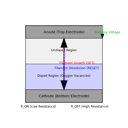
Memristors, postulated by Leon Chua in 1971 as the fourth fundamental circuit element, exhibit a unique relationship between charge q and flux linkage φ. Their resistance state depends on the history of applied voltage and current, making them non-volatile memory candidates. The constitutive relation is expressed as:
where M(q) represents the memristance, with units of ohms (Ω). When implemented using metal-oxide thin films (e.g., TiO2), oxygen vacancy migration modulates the device resistance. The linear drift model approximates this behavior:
Here, w(t) is the doped region width, D the total film thickness, and RON/ROFF the minimum/maximum resistance states.
RRAM Device Physics
Practical RRAM cells implement memristive switching through filament formation/rupture in transition metal oxides. The SET process (low-resistance state) occurs when a forming voltage creates conductive filaments via electrochemical reactions. RESET (high-resistance state) dissolves these filaments through Joule heating. Key parameters include:
- Switching threshold voltage (1-3 V typical)
- Endurance (>106 cycles for industrial-grade devices)
- Retention time (>10 years at 85°C)
Neuromorphic Applications
Memristors naturally emulate synaptic plasticity. The conductance G can represent synaptic weight, modifiable via spike-timing-dependent plasticity (STDP). For two neurons A and B, the weight update follows:
where Δt = tpost - tpre is the spike timing difference. Crossbar arrays of RRAM devices enable efficient matrix-vector multiplication for neural networks, achieving O(1) complexity for weight updates compared to O(N2) in digital implementations.
Fabrication Challenges
Despite promising characteristics, RRAM faces variability issues due to:
- Stochastic filament formation (20-30% cycle-to-cycle variation)
- Temperature-dependent switching kinetics
- Electrode/oxide interface reactions
3D integration approaches using vertical pillars and selector devices (1S1R configuration) are being developed to address density limitations while maintaining performance.
2.2 Spiking Neural Networks (SNNs)
Biological Foundations of SNNs
Spiking Neural Networks (SNNs) derive their computational principles from biological neurons, which communicate via discrete electrical pulses called action potentials or spikes. Unlike traditional artificial neurons that use continuous activations, SNNs encode information in the timing and frequency of spikes, closely mimicking neural dynamics in the brain. Key biological features replicated in SNNs include:
- Temporal coding: Information is represented by spike timing (e.g., latency or inter-spike intervals).
- Leaky integrate-and-fire (LIF) dynamics: Neurons integrate input currents and fire when a threshold is reached.
- Synaptic plasticity: Spike-timing-dependent plasticity (STDP) adjusts synaptic weights based on spike correlations.
Mathematical Model of Spiking Neurons
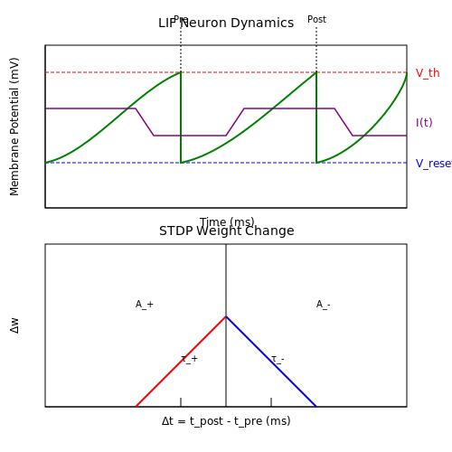
The LIF neuron, the most widely used SNN model, is governed by a differential equation describing membrane potential V(t):
where τm is the membrane time constant, Vrest is the resting potential, Rm is membrane resistance, and I(t) is input current. When V(t) crosses a threshold Vth, a spike is emitted, and V(t) resets to Vreset.
Event-Driven Computation
SNNs operate asynchronously, processing spikes only when they occur. This contrasts with conventional artificial neural networks (ANNs) that perform layer-wise synchronous computations. Event-driven processing enables:
- Energy efficiency: Computation occurs only during spikes, reducing power consumption.
- Low-latency responses: Early spikes can trigger rapid decisions without waiting for full network convergence.
Spike-Timing-Dependent Plasticity (STDP)
STDP is a biologically inspired unsupervised learning rule where synaptic weight changes depend on the relative timing of pre- and postsynaptic spikes. The weight update Δw is given by:
Here, Δt = tpost - tpre is the spike timing difference, and A±, τ± control the magnitude and time window of plasticity.
Hardware Implementations
SNNs are implemented in neuromorphic hardware like Intel's Loihi and IBM's TrueNorth, which emulate spiking dynamics at scale. These architectures feature:
- Massive parallelism: Thousands of neurons operate concurrently.
- On-chip learning: STDP and other rules are hardware-accelerated.
- Low-power operation: Event-driven logic minimizes energy use.
Applications and Challenges
SNNs excel in tasks requiring temporal processing, such as:
- Real-time sensory processing: Vision (event cameras), auditory systems.
- Robotic control: Adaptive motor control with millisecond latency.
Challenges include training complexity due to non-differentiable spike events and the lack of standardized software frameworks.
2.3 Event-Driven Processing and Asynchronous Circuits
Fundamentals of Event-Driven Processing
Event-driven processing in neuromorphic systems operates on the principle that computations are triggered only when an input change (event) occurs, rather than following a fixed clock cycle. This approach mirrors biological neural networks, where spikes (events) drive information processing. The absence of a global clock eliminates synchronous overhead, reducing power consumption and enabling real-time responsiveness.
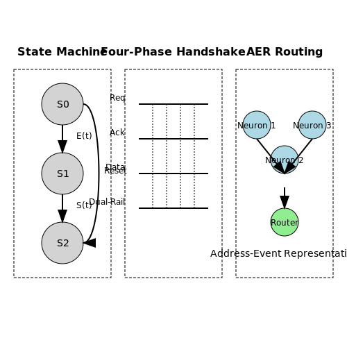
The mathematical representation of an event-driven system can be modeled as a state machine where transitions occur upon event arrival. Let the system state S evolve according to:
where E(t) represents the incoming event at time t, and f is the state transition function. Unlike synchronous systems where Δt is fixed by a clock period, in event-driven systems, Δt is determined by the inter-event interval.
Asynchronous Circuit Design Principles
Asynchronous circuits implement event-driven processing through several key design paradigms:
- Handshake protocols: Four-phase or two-phase signaling ensures reliable communication between modules without global timing references.
- Delay-insensitive coding: Uses codes like dual-rail or one-hot encoding where data validity is self-timed.
- Quasi-delay-insensitive (QDI) logic: Circuits remain functional regardless of gate delays, except for specific isochronic forks.
The metastability risk in asynchronous circuits is quantified by the mean time between failures (MTBF):
where τ is the resolving time constant, τc is the metastability time constant of the technology node, and fevent, fclock are the event and sampling frequencies.
Neuromorphic Implementations
Modern neuromorphic chips like Intel's Loihi and ETH Zurich's BrainScaleS employ event-driven processing through:
- Address-event representation (AER): Neurons communicate via digital spikes carrying source/destination addresses.
- Asynchronous crossbars: Non-blocking routing fabrics that propagate events with nanosecond latency.
- Dynamic power gating: Circuits remain idle until activated by incoming events, achieving sub-threshold power consumption.
The energy per spike in such systems follows:
where Ctotal is the switched capacitance, Vdd is the supply voltage, and tactive is the duration of post-event activity.
Challenges and Trade-offs
While event-driven processing offers significant advantages in power efficiency and real-time performance, several challenges persist:
- Verification complexity: The absence of a clock makes formal verification and timing analysis substantially harder.
- Event collision handling: Arbitration circuits add overhead when multiple events arrive simultaneously.
- Process variation sensitivity: Asynchronous designs are more susceptible to manufacturing variations due to their reliance on analog timing.
Recent advances in stochastic computing and approximate computing have shown promise in mitigating these issues while maintaining the energy benefits of asynchronous operation.
3. Spike-Timing-Dependent Plasticity (STDP)
3.1 Spike-Timing-Dependent Plasticity (STDP)
Spike-Timing-Dependent Plasticity (STDP) is a biologically inspired synaptic learning rule that adjusts synaptic strength based on the precise timing of pre- and postsynaptic spikes. It is a form of Hebbian learning, where synaptic efficacy is modified according to the temporal correlation between neuronal activity. The foundational principle of STDP is captured by the following weight update rule:
Here, Δw represents the change in synaptic weight, Δt = tpost - tpre is the time difference between spikes, A+ and A- are the maximum potentiation and depression amplitudes, and τ+ and τ- are the time constants governing the exponential decay.
Biological Basis of STDP
STDP was first experimentally observed in hippocampal and cortical neurons, where long-term potentiation (LTP) and long-term depression (LTD) were found to depend on millisecond-scale spike timing. The underlying mechanisms involve:
- NMDA receptor activation – Critical for LTP when presynaptic input precedes postsynaptic firing.
- Calcium influx dynamics – High calcium concentrations trigger LTP, while moderate levels induce LTD.
- Backpropagating action potentials (bAPs) – Postsynaptic spikes traveling back into dendrites influence synaptic plasticity.
Mathematical Derivation of STDP
The STDP learning window can be derived from first principles by modeling synaptic dynamics as a differential equation. Let w(t) denote the synaptic weight at time t, and let s(t) represent the spike train of a neuron:
The weight update is governed by a pair-based STDP rule, where the change depends on the spike pairs between pre- and postsynaptic neurons. The integral form of the weight update is:
where W(Δt) is the STDP learning window function, defined as:
Applications in Neuromorphic Computing
STDP is widely used in neuromorphic hardware due to its locality and event-driven nature, making it suitable for low-power, real-time learning. Key applications include:
- Spiking Neural Networks (SNNs) – STDP enables unsupervised feature learning in pattern recognition tasks.
- Memristor-based synapses – Analog resistive memory devices naturally emulate STDP due to their conductance modulation properties.
- Robotic control – Adaptive motor learning in robotic systems via spike-based reinforcement.
Variants and Extensions of STDP
Several modifications to the basic STDP rule have been proposed to enhance functionality:
- Triplet STDP – Incorporates interactions among multiple spikes to better fit experimental data.
- Voltage-based STDP – Considers postsynaptic membrane potential instead of spike timing alone.
- Homeostatic STDP – Balances synaptic changes to prevent runaway excitation or depression.
Recent advances in neuromorphic chips, such as Intel's Loihi and IBM's TrueNorth, implement STDP in hardware, enabling energy-efficient learning at the edge.
3.2 Neuromorphic Learning Rules
Spike-Timing-Dependent Plasticity (STDP)
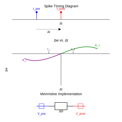
Spike-Timing-Dependent Plasticity (STDP) is a biologically inspired learning rule where synaptic weight changes depend on the precise timing of pre- and postsynaptic spikes. If a presynaptic neuron fires before the postsynaptic neuron, the synapse is strengthened (long-term potentiation, LTP). Conversely, if the firing order is reversed, the synapse weakens (long-term depression, LTD). The weight update rule is typically modeled as:
Here, Δw is the synaptic weight change, Δt = tpost - tpre is the spike timing difference, and A±, τ± govern the magnitude and time constants of LTP/LTD. This asymmetric Hebbian rule enables unsupervised feature extraction in spiking neural networks (SNNs).
Reward-Modulated STDP (R-STDP)
R-STDP extends STDP by incorporating global reward signals to guide learning. The weight update is modulated by a reward prediction error δ, derived from dopamine-like reinforcement signals:
where η is the learning rate and ΔwSTDP is the baseline STDP update. This enables policy gradient learning in neuromorphic systems, bridging unsupervised plasticity with goal-directed behavior. Applications include robotic control and adaptive decision-making.
Local vs. Global Learning Rules
Neuromorphic systems balance local (synapse-specific) and global (network-wide) learning. Local rules like STDP operate autonomously at synapses, minimizing communication overhead. Global rules, such as backpropagation-through-time (BPTT) approximations, require external error propagation but achieve higher accuracy. Hybrid approaches, like e-prop, combine local eligibility traces with global credit assignment:
Here, eij(t) is a local eligibility trace, and ∇wijℒ is the global loss gradient. This trade-off is critical for scalable on-chip learning.
Memristive Synaptic Plasticity
In hardware implementations, resistive memory (memristor) devices emulate synaptic weights. The conductance G of a memristor updates via voltage pulses, mimicking STDP:
where Vpre and Vpost are presynaptic and postsynaptic spike waveforms. Non-ideal effects like conductance drift and device variability must be compensated using adaptive pulse schemes.
Energy-Efficient Learning
Neuromorphic chips prioritize energy efficiency by exploiting sparse, event-driven updates. For example, Intel’s Loihi processor implements STDP with 1–10 pJ per synaptic operation, outperforming conventional GPUs by 1000× in energy-per-synapse metrics. Key optimizations include:
- Analog-mixed-signal circuits for in-memory computing.
- Time-domain signal processing to avoid multi-bit ADCs.
- Approximate gradient calculations for backpropagation.
These techniques enable real-time learning in edge devices with milliwatt power budgets.
3.3 Applications in Pattern Recognition and Robotics
Neuromorphic Vision for Real-Time Pattern Recognition
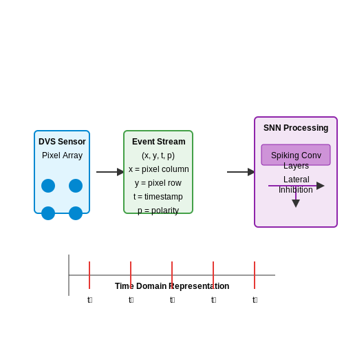
Event-based vision sensors, such as dynamic vision sensors (DVS), leverage neuromorphic principles to capture visual information asynchronously, only responding to changes in pixel intensity. This contrasts with traditional frame-based cameras, reducing latency and power consumption. The output is a stream of events (x, y, t, p), where x, y denote pixel location, t is the timestamp, and p is the polarity (brightness increase or decrease).
Spiking neural networks (SNNs) process these events using biologically inspired mechanisms. A key advantage is their ability to recognize temporal patterns in data streams, making them ideal for tasks like gesture recognition or object tracking. For instance, IBM's TrueNorth chip achieves 2000 fps object detection at just 300 mW by exploiting sparse, event-driven computation.
Robotic Control with Adaptive Neuromorphic Systems
Neuromorphic processors enable robots to perform complex tasks with low power and high efficiency. A prominent example is the integration of Intel's Loihi chip into robotic arms for real-time adaptive control. The system uses spike-timing-dependent plasticity (STDP) to learn from sensory feedback:
where wij is the synaptic weight between neurons i and j, η is the learning rate, and τ is the time constant. This allows the robot to adjust grip force dynamically when handling fragile objects, demonstrating millisecond-level response times.
Case Study: Autonomous Navigation
In 2022, researchers at ETH Zurich deployed a neuromorphic drone that processes optic flow data using an SNN on a neuromorphic chip. The system consumes 5 W while performing obstacle avoidance at 30 m/s, compared to 50 W for an equivalent GPU-based solution. The network architecture consists of:
- Input layer: 64×64 pixel DVS sensor array
- Hidden layers: 3 spiking convolutional layers with lateral inhibition
- Output layer: 6 motor neurons controlling thrust and yaw
Tactile Sensing and Manipulation
Recent advances in neuromorphic tactile sensors (e.g., the NeuroTac sensor) provide robots with human-like touch perception. These sensors encode pressure changes as spike trains, with temporal coding preserving information about contact dynamics. A robotic hand using such sensors can distinguish between 20 different textures with 94% accuracy while consuming <1 mW per taxel (tactile element).
4. Scalability and Fabrication Issues
4.1 Scalability and Fabrication Issues
Neuromorphic systems face significant challenges in scaling to biologically plausible neuron counts while maintaining energy efficiency and functional fidelity. The primary bottlenecks stem from device physics, interconnect complexity, and thermal management constraints.
Device-Level Scaling Limitations
Memristive synapses and spiking neurons must achieve sub-100nm feature sizes to match biological density (~104 synapses/neuron). The Landauer limit imposes a fundamental energy bound:
However, practical CMOS-memristor hybrids currently operate at ~10fJ/spike due to:
- Parasitic capacitances in crossbar arrays
- Non-ideal ion transport in resistive RAM
- Leakage currents in subthreshold circuits
Interconnect Bottlenecks
The Rent's Rule exponent p for neuromorphic architectures typically falls between 0.6-0.8, leading to wire length distributions that follow:
where N is the number of components. For a 1cm2 chip with 108 neurons, this results in:
3D integration with through-silicon vias (TSVs) partially mitigates this, but introduces new thermal challenges.
Thermal Constraints
Power density in analog neuromorphic chips follows:
where ρsyn is synaptic density (107/mm2 for biological targets). At 1Hz global activity, this already reaches:
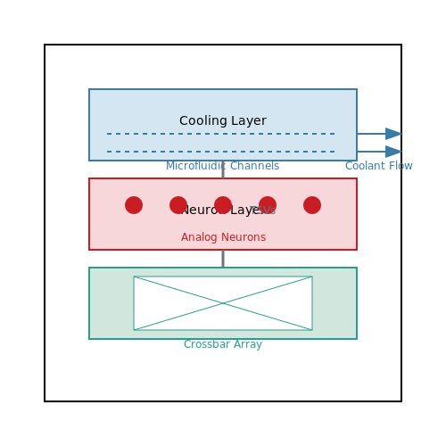
Advanced cooling solutions like microfluidic channels become necessary beyond wafer-scale integration.
Process Variation Effects
Threshold voltage (Vth) mismatch in sub-20nm transistors introduces neuronal timing jitter:
where gm is transconductance. For typical 65nm processes:
This necessitates calibration circuits consuming >20% of die area in current designs.
Emerging Fabrication Approaches
Recent advances address these issues through:
- Ferroelectric FETs (FeFETs): 5nm-thick HfZrO2 gates enable 106 endurance cycles at 0.4V operation
- Monolithic 3D integration: Stacked tiers with 1μm pitch TSVs demonstrate 4Tbit/s/mm2 inter-layer bandwidth
- Self-assembled nanowires: DNA-guided growth achieves 8nm pitch alignment (vs. 32nm EUV lithography limit)
4.2 Energy Efficiency vs. Computational Power
Neuromorphic systems achieve remarkable energy efficiency by mimicking the sparse, event-driven computation of biological neural networks. Unlike conventional von Neumann architectures, where energy is continuously dissipated through clock-driven switching, neuromorphic chips operate predominantly in the subthreshold regime, leveraging the physics of analog computation to minimize power consumption. The energy per synaptic event Esyn in a typical neuromorphic circuit can be expressed as:
where Csyn is the synaptic capacitance and Vdd the supply voltage. Operating in weak inversion (subthreshold) reduces Vdd to the order of thermal voltage (≈26 mV at 300 K), yielding energy efficiencies below 1 pJ per spike – two to three orders of magnitude better than digital CMOS implementations.
Tradeoffs in Parallelism vs. Precision
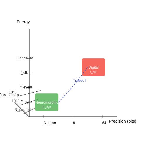
The energy advantage comes with fundamental tradeoffs between parallelism and numerical precision. Biological neurons achieve robustness through massive parallelism with 4-8 bit effective precision, whereas digital systems rely on 32-64 bit precision with sequential processing. The energy-quality scaling follows:
where Nbits is the bit precision, fclk the clock frequency, Nparallel the number of parallel units, and fevent the average spike rate. IBM's TrueNorth chip demonstrated this tradeoff practically, achieving 46 billion synaptic operations per second at 70 mW by employing 1 million neurons with binary synapses.
Leakage Power Dominance in Scaled Technologies
Below 28 nm process nodes, static leakage power becomes comparable to dynamic switching energy in digital implementations. Neuromorphic circuits counter this through:
- Voltage scaling - Operating near or below threshold voltage (≈300 mV in 28 nm)
- Asynchronous design - Eliminating clock distribution networks that contribute 30-40% of digital power
- Event-driven sparsity - Only active neurons consume significant power
The table below compares measured energy efficiencies across architectures:
| Architecture | Precision | Energy/Op (J) | Throughput (OPS/W) |
|---|---|---|---|
| GPU (NVIDIA A100) | FP16 | 1e-12 | 1e12 |
| Neuromorphic (Loihi 2) | 4-bit | 1e-15 | 1e15 |
| Biological Neuron | ≈3-bit | 1e-16 | 1e16 |
Thermodynamic Limits of Neural Computation
The Landauer limit sets the minimum energy for irreversible computation at kT ln(2) ≈ 2.9 zJ at room temperature. While no practical system reaches this bound, neuromorphic approaches come closer than digital alternatives by:
State-of-the-art neuromorphic chips achieve η ≈ 104, compared to η ≈ 108 for conventional processors. Further improvements require near-reversible computing techniques and cryogenic operation.
Applications in Edge AI
This energy-proportional computing enables always-on edge devices. For example, Intel's Loihi 2 demonstrates real-time gesture recognition at 30 mW – three orders of magnitude more efficient than equivalent GPU implementations. The key architectural features enabling this include:
- Analog dendritic accumulators replacing digital multiply-accumulate units
- Dynamic voltage-frequency scaling based on workload
- Stochastic rounding for graceful precision degradation
4.3 Integration with Conventional Computing Systems
Architectural Challenges
Integrating neuromorphic systems with conventional von Neumann architectures introduces fundamental challenges due to divergent computational paradigms. While von Neumann systems rely on sequential, clock-driven processing with centralized memory, neuromorphic designs operate via event-driven, massively parallel spiking neural networks (SNNs) with distributed memory. Bridging this gap requires addressing:
- Data representation mismatch: Conventional systems process discrete binary data, whereas neuromorphic chips encode information in spike timing (temporal coding) or rate (rate coding).
- Latency synchronization: Asynchronous neuromorphic events must interface with synchronous CPU/GPU clock domains, necessitating buffering or adaptive clocking.
- Memory access: Von Neumann architectures suffer from the memory wall, while neuromorphic systems minimize data movement via in-memory computing.
Hybrid System Design Approaches
Three primary integration strategies have emerged, each with trade-offs in programmability, energy efficiency, and throughput:
1. Co-Processing Acceleration
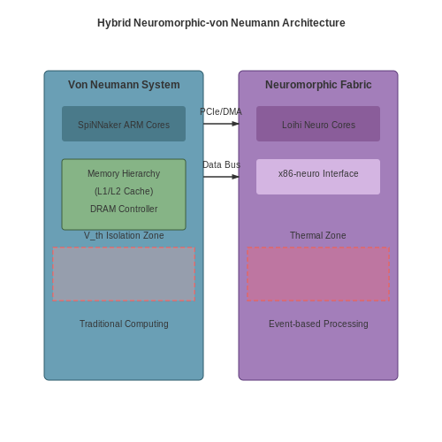
Neuromorphic chips act as accelerators for specific tasks (e.g., real-time pattern recognition) while CPUs handle control flow. The SpiNNaker system exemplifies this, where ARM cores manage spike routing between neuromorphic cores. The interface latency L between host and accelerator follows:
where Nspikes is spike count, tcomm is per-spike communication overhead, B is bus bandwidth, and tsync is synchronization delay.
2. Tightly Coupled Heterogeneous Cores
Recent SoCs (e.g., Intel Loihi 2) integrate x86 cores with neuromorphic fabric on-die, enabling shared memory access. This reduces latency but requires novel cache coherence protocols to handle spiking traffic. The energy per operation Ehybrid scales as:
where α is the fraction of workload offloaded to neuromorphic cores.
3. Software-Defined Virtualization
Frameworks like Lava (Intel) abstract neuromorphic hardware as parallel processes, allowing conventional code to interact via APIs. This sacrifices some energy efficiency for programmability, with typical overheads of 15-30% compared to native execution.
Case Study: IBM TrueNorth Integration
IBM's TrueNorth was deployed in Lawrence Livermore National Lab's CORAL supercomputer, interfacing with Power9 CPUs via PCIe. Key metrics:
- 28 mW power for real-time video classification (vs. 150W for GPU equivalent)
- 1.2 μs spike latency across the host-accelerator boundary
- 12 Gbps sustained spike throughput using custom DMA engines
Emerging Standards
The Neuromorphic Computing Interface Standardization Group (NCSG) is developing protocols for:
- Spike packetization (adopting Ethernet-like headers with timestamps)
- Cross-platform neural network description languages (e.g., PyNN)
- Benchmark suites for hybrid systems (MLPerf Neuromorphic)
Thermal and Power Considerations
Neuromorphic chips operating near threshold voltage (Vth) require careful power domain isolation when interfaced with conventional logic. A typical integration must satisfy:
where k is thermal conductivity, A is die area, and Cth is heat capacity. Solutions include:
- Active cooling zones between digital and analog blocks
- Dynamic voltage scaling synchronized with spike bursts
5. Key Research Papers and Journals
5.1 Key Research Papers and Journals
- Device and materials requirements for neuromorphic computing — [1] Mead C 1990 Neuromorphic electronic systems Proc. IEEE 78 1629-36 Crossref; Google Scholar [2] Horowitz M 2014 1.1 computing's energy problem (and what we can do about it) IEEE Int. Solid-State Circuits Conf. Digest of Technical Papers pp 10-14 Google Scholar [3] Ando K et al. 2017 BRein memory: a 13-layer 4.2 K neuron/0.8 M synapse binary/ternary reconfigurable in-memory deep neural ...
- Recent advances in emerging neuromorphic computing and perception ... — Brain-inspired electronics represent a promising paradigm to resolve the energy and time bottlenecks in conventional digital machines. Recent advances have spanned both computing and sensing by imitating naturally evolved biological approaches, and the emerging neuromorphic computing and perception devices are recognized as the building blocks for implementing so-called in-memory and in-sensor ...
- High Linearity and Symmetry Ferroelectric Artificial Neuromorphic ... — 1 Introduction. With the vigorous development of artificial intelligence (AI) technology, the traditional von Neumann system cannot meet the needs of simultaneously completing the storage and computing functions of a large amount of data. [] The human brain, with 10 11 neurons and 10 15 synapses, is excellent at information processing and requires a low consumption ≈20 fJ. []
- Neuromorphic computing's yesterday, today, and tomorrow - an ... — Neuromorphic algorithms are able to learn functions from training dataset and can be roughly divided into artificial neural network (ANN) and spiking neural network (SNN), where data is represented as numerical values [2] or spikes [3], respectively.Very similar to biologic neural networks, synapses and neurons are often two basic units in the neuromorphic algorithms to manipulate the data and ...
- Artificial synapses enabled neuromorphic computing: From blueprints to ... — Emerging brain-inspired neuromorphic computing systems have become a potential candidate for overcoming the von Neuman bottleneck that limits the performance of most modern computers. ... By the end of this review, we discuss the engineering issues including control methods, design complexity and fabrication process to be addressed, and ...
- Frontiers | Considerations for Neuromorphic Supercomputing in ... — Semiconductor systems benefit from a robust fabrication ecosystem and can build on extensive progress made in purely electronic neuromorphic computing but will require III-V light source integration with electronics at an unprecedented scale, further advances in ultra-low capacitance photodiodes, and success from emerging memory technologies.
- Emerging memristive neurons for neuromorphic computing and sensing — Beyond neuromorphic computing application, memristive neurons have also been used to construct human-like interactive neuromorphic sensing computing system. By using perception computing system based on artificial memristive neurons, continuous analog sensing signals from the environment can be converted into discrete spike signals without ...
- Bio-inspired artificial synapses: Neuromorphic computing chip ... — The engineering of neuromorphic computing chips using soft biomaterials is a fascinating area that is growing quickly. In addition to highlighting the research gap in the use of these materials in chip designs, this perspective gives a summary of the current state of the area [13]. The review also highlights the most encouraging advancements in ...
- Neuromorphic Computing in Neuroscience: Mimicking the Brain's — Functionality Noman hameed Punjab medical helth centre of readiology, univerist of PM Abstract Neuromorphic computing, a paradigm inspired by the structure and functioning of the human brain, has ...
- Neuromorphic Engineering: In Memory of Misha Mahowald — Making an electronic system that operates with events the way the brain does should be possible. Fortunately, the availability of event-sensor systems gives us data to work with. The topic has become the center of a growing, vibrant research community. It is prominent in the Neuromorphic Roadmap (Christensen et al., 2022).
5.2 Books on Neuromorphic Engineering
- PDF Neuromorphic Engineering; The Scientist s, Algorithm Designer s, and ... — 10.3 MEMRISTORS FOR NEUROMORPHIC ENGINEERING 181 10.4 GLOSSARY 183 10.5 FURTHER READING 183 Section IV The Algorithms Designer's Perspective Chapter11 Introduction to neuromorphic programming 187 11.1 THEORY OF NEUROMORPHIC COMPUTING 187 11.1.1 Neuromorphic computing as Turing complete 187 11.1.2 A complexity theory for neuromorphic computing 189
- 2022 roadmap on neuromorphic computing and engineering — The aim of this roadmap is to present a snapshot of the present state of neuromorphic technology and provide an opinion on the challenges and opportunities that the future holds in the major areas of neuromorphic technology, namely materials, devices, neuromorphic circuits, neuromorphic algorithms, applications, and ethics.
- Neuromorphic Computing between Reality and Future Needs — Neuromorphic computing is a one of computer engineering methods that to model their elements as the human brain and nervous system. Many sciences as biology, mathematics, electronic engineering, computer science and physics have been integrated to construct artificial neural systems. In this chapter, the basics of Neuromorphic computing together with existing systems having the materials ...
- Event-Based Neuromorphic Systems[Book] - O'Reilly Media — This pioneering text is an indispensable resource for practicing neuromorphic electronic engineers, advanced electrical engineering and computer science students and researchers interested in neuromorphic systems. Key features: Summarises the latest design approaches, applications, and future challenges in the field of neuromorphic engineering.
- Neuromorphic Computing: A Path to Artificial Intelligence Through ... — Neuromorphic computing emulates the physical structure of neural systems using an approach of software and hardware co-design that potentially can offer a more ... 5(2), 173 (1965) ... An electronic neuromorphic system for real-time detection of high frequency oscillations (HFO) in intracranial EEG. Nat. Commun. 12(1), 1-14 (2021) Article ...
- Event-based neuromorphic systems / | Round Rock Public Library — "Neuromorphic electronic engineering takes its inspiration from the functioning of nervous systems to build more power efficient electronic sensors and processors. Event-based neuromorphic systems are inspired by the brain's efficient data-driven communication design, which is key to its quick responses and remarkable capabilities. This cross-disciplinary text establishes how circuit building ...
- Neuromorphic Circuits and Systems: From Neuron Models to ... - Springer — Neuromorphic systems have a wide range of applications. There has been recent research in designing visual processors that can be coupled with autonomous mobile systems such as drones and unmanned aerial vehicles (UAVs), micro aerial vehicles (MAVs), and self-driving cars for efficient navigation, object detection, and object recognition [5,6,7] as seen in Fig. 2.
- Neuromorphic Hardware Accelerators - SpringerLink — One of the most promising approaches is neuromorphic computing, which takes direct inspiration from the structure of a biological neuron. ... Three basic circuit elements, that is, resistors, capacitors, and inductors, form the basis of all electronic systems, including semiconductors. ... Engineering Engineering (R0) Share this chapter.
- Neuromorphic photonic networks using silicon photonic weight banks - Nature — A key benefit of neuromorphic engineering is that existing algorithms can be leveraged. A subset of CTRNNs, Hopfield networks 68 , have been used extensively in mathematical programming and ...
- Bio-inspired artificial synapses: Neuromorphic computing chip ... — The engineering of neuromorphic computing chips using soft biomaterials is a fascinating area that is growing quickly. In addition to highlighting the research gap in the use of these materials in chip designs, this perspective gives a summary of the current state of the area [13]. The review also highlights the most encouraging advancements in ...
5.3 Online Resources and Tutorials
- PDF Neuromorphic Engineering; The Scientist s, Algorithm Designer s, and ... — 10.3 MEMRISTORS FOR NEUROMORPHIC ENGINEERING 181 10.4 GLOSSARY 183 10.5 FURTHER READING 183 Section IV The Algorithms Designer's Perspective Chapter11 Introduction to neuromorphic programming 187 11.1 THEORY OF NEUROMORPHIC COMPUTING 187 11.1.1 Neuromorphic computing as Turing complete 187 11.1.2 A complexity theory for neuromorphic computing 189
- PDF Neuromorphic Computing - u-aizu.ac.jp — Neuromorphic Computing Ben Abdallah Abderazek, Khanh N. Dang E-mail: {benab, khanh}@u-aizu.ac.jp This lecture is based on the book ''Neuromorphic Computing Principles and Organization,''Publisher: Springer; 2022 edition,ISBN-10:3030925242, ISBN-13:978-3030925246, by Abderazek Ben Abdallah, Khanh N. Dang 5. Communication Networks
- Neuromorphic Computing between Reality and Future Needs — Neuromorphic computing is a one of computer engineering methods that to model their elements as the human brain and nervous system. Many sciences as biology, mathematics, electronic engineering, computer science and physics have been integrated to construct artificial neural systems. In this chapter, the basics of Neuromorphic computing together with existing systems having the materials ...
- PDF ENERGY-EFFICIENT NEUROMORPHIC COMPUTING - University of Michigan — Wiley also publishes its books in a variety of electronic formats and by print-on-demand. Some content that appears in standard print versions of this ... Learning in Energy-Efficient Neuromorphic Computing: Algorithm and Architecture Co-Design In 1987 when I was wrapping up my doctoral thesis at the University of Illinois, I had a
- Is Neuromorphic Computing the Key to Power-Efficient Neural ... - Springer — Neuromorphic computing is a type of computing that is modelled after the human brain. It is designed to mimic the neural networks of the brain, which are made up of interconnected neurons that communicate through electrical impulses. ... 5.3 Resource Analysis and Discussion. ... College of Electronic and Information Engineering, Nanjing ...
- EPOC: A 28-nm 5.3 pJ/SOP Event-driven Parallel Neuromorphic Hardware ... — Bio-inspired neuromorphic hardware with learning ability is highly promising to achieve human-like intelligence, particularly in terms of high energy efficiency and strong environmental adaptability. Though many customized prototypes have demonstrated learning ability, learning on neuromorphic hardware still lacks a bio-plausible and unified learning framework, and inherent spike-based ...
- Event-based neuromorphic systems / | Round Rock Public Library — "Neuromorphic electronic engineering takes its inspiration from the functioning of nervous systems to build more power efficient electronic sensors and processors. Event-based neuromorphic systems are inspired by the brain's efficient data-driven communication design, which is key to its quick responses and remarkable capabilities. This cross-disciplinary text establishes how circuit building ...
- Neuromorphic Computing Explained | Baeldung on Computer Science — Neuromorphic computing, however, offers solutions to some limitations by borrowing from the architecture of the human brain. In this tutorial, we'll discuss the fundamentals of neuromorphic computing, explaining how it works and its importance. We'll also provide a practical use case to illustrate its application. 2.
- PyNCS: a microkernel for high-level definition and configuration of ... — 1.1. Software ecosystems for neuromorphic electronic computing platforms. Several software platforms for controlling neuromorphic systems have already been developed. For example, the jAER software (jAER, 2006) is an open-source project, written in Java, that allows soft real-time processing of event-based data from spiking neuromorphic chips.