Eagle CAD
1. What is Eagle CAD?
1.1 What is Eagle CAD?
Eagle CAD, developed by Autodesk, is a powerful and widely used electronic design automation (EDA) software. It provides users with tools for both schematic capture and printed circuit board (PCB) layout, enabling engineers, researchers, and hobbyists alike to design and prototype electronic circuits effectively. Eagle CAD's versatility has made it a preferred choice for professionals and students who require a robust platform for circuit design.
The software allows users to create complex electronic systems through its schematic editor, which supports multi-sheet projects, hierarchical designs, and extensive libraries filled with components ranging from resistors to integrated circuits. Once a schematic is complete, the PCB layout editor comes into play, providing a platform for placing components, routing traces, and defining layers of the PCB.
Practical Applications
Eagle CAD is employed in various domains—all the way from education to industry. In academia, students use it to learn the fundamentals of circuit design, while in industry, it's used to produce professional-grade schematic diagrams and PCBs for consumer electronics, automotive systems, and more. The software's integration capabilities with simulation tools allow for testing and validation of designs even before physical prototypes are produced, enhancing the reliability and performance of electronic systems.
Capabilities and Features
- Schematic Editor: The intuitive interface allows drag-and-drop component placement and easy manipulation of circuit connections.
- Library Management: Users can access extensive libraries of components and create custom components as needed for specific applications.
- PCB Layout Editor: Offers features such as auto-router and interactive routing, enhancing design efficiency.
- Design Rule Check (DRC): Ensures that PCB designs conform to manufacturing specifications, reducing errors before production.
The ability of Eagle CAD to handle both schematic and PCB design in a single integrated environment sets it apart from simpler design tools. As projects grow in complexity, the seamless transition from schematic to layout becomes crucial in saving time and maintaining design integrity.
In summary, Eagle CAD is not just a tool but an essential component of the electronic design engineering toolkit, bridging the gap between conceptualization and physical realization of electronic circuits.
1.2 Key Features and Benefits
Eagle CAD, a powerful and widely used Electronic Design Automation (EDA) tool, offers engineers and researchers a suite of advanced features tailored for PCB design and schematic capture. Understanding these features is essential for maximizing efficiency throughout the design cycle, from conceptualization to prototype development. Below, we explore some of the most significant capabilities of Eagle CAD, highlighting their practical applications.Robust Schematic Capture
One of the standout features of Eagle CAD is its robust schematic capture capability. It provides a user-friendly interface that allows designers to create complex circuit diagrams with ease. The software supports hierarchical designs, enabling users to divide circuits into manageable sub-blocks, which can be reused across multiple projects. This hierarchical structure not only simplifies the design process but also enhances collaboration among team members, as separate teams can work on different parts of a larger project without interference. Furthermore, designers can easily annotate their schematics with notes and comments, providing necessary context for future modifications.Extensive Component Library
Eagle CAD boasts a comprehensive library of electronic components, including resistors, capacitors, ICs, and even custom components. This library is continuously updated, ensuring that users have access to the latest parts from manufacturers. Moreover, users have the option to create and integrate their custom components, which can be invaluable in specialized applications, such as unique sensor configurations or bespoke circuitry. The ease of searching and filtering through the library aids significantly in reducing design time. Users can quickly find components based on specifications, manufacturing part numbers, or even the component’s footprint.Powerful PCB Layout Tools
Transitioning from schematic to PCB layout in Eagle CAD is streamlined, allowing for efficient design progression. The software features an intuitive drag-and-drop interface that aids users in placing components, adjusting layouts, and routing traces. Routing capabilities are particularly advanced, with options for auto-routing and manual routing available. The auto-router can quickly generate trace connections based on several constraints, optimizing the layout for performance and manufacturability. Additionally, the software includes design rule checks (DRCs) that prevent common layout errors, such as trace width violations and overlap issues. This ensures that the final design adheres to both electrical and mechanical specifications, facilitating a smoother transition to fabrication.3D Visualization and Export
Eagle CAD includes a 3D visualization feature that allows users to view their PCB designs in three dimensions. This is particularly beneficial for verifying mechanical fit and assessing potential assembly issues before manufacturing begins. Users can rotate and zoom into their designs, closely inspecting component placements and ensuring that there are no hidden conflicts. Furthermore, users can export their designs in various formats, including Gerber files, which are essential for PCB manufacturing, and other industry-standard formats that enable smooth collaboration with fabrication facilities.Integration with Other Tools
Eagle CAD's ability to integrate with other design tools enhances its utility in modern engineering workflows. For instance, users can import designs from Fusion 360 for mechanical assemblies, ensuring that both electrical and mechanical constraints are acknowledged in the design phase. Additionally, Eagle CAD supports export to simulation software, enabling engineers to validate their circuit designs in virtual environments before committing to physical prototypes. This integration with a broader ecosystem of tools illustrates how Eagle CAD can fit within various stages of product development.Collaboration and Cloud Capabilities
In an era of remote work and global teams, Eagle CAD's collaboration features cannot be overlooked. Users can share their designs and libraries via the cloud, allowing for real-time collaboration. This capability is especially advantageous for teams that operate across different geographical locations. By utilizing version control and sharing tools, design iterations can be tracked efficiently, preventing the loss of critical data during the design process and fostering a coordinated approach to project development. In conclusion, Eagle CAD offers a rich set of features that not only enhance individual productivity but also promote collaboration and efficiency in team environments. Understanding and utilizing these tools effectively can lead to more innovative designs, reduced time to prototype, and ultimately, successful product development in the fast-paced world of electronics.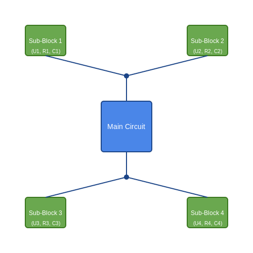
1.3 System Requirements and Installation
In the realm of electronic design automation (EDA), Eagle CAD serves as a pivotal tool, particularly for engineers and researchers entrenched in circuit design and PCB layout. Understanding the system requirements for installing Eagle CAD is crucial for a seamless experience, ensuring that the software operates efficiently on your hardware. Whether you are a seasoned engineer managing complex circuitry or a researcher developing prototype boards, being aware of the specifications can make a significant difference in productivity.
Hardware Requirements
To run Eagle CAD optimally, the following hardware specifications are recommended:
- Processor: A multi-core processor (minimum dual-core) running at 2.0 GHz or faster. This enables efficient processing of complex designs without lag.
- Memory (RAM): At least 8 GB is advisable, though 16 GB is preferred for more extensive projects involving multiple layers and components.
- Storage: A minimum of 5 GB of available disk space, with solid-state drives (SSDs) providing faster read/write operations, thus expediting the loading of large files.
- Graphics: A dedicated graphics card can improve rendering performance, particularly for 3D viewing of layouts and schematics.
- Display: A resolution of 1920 x 1080 or higher is beneficial for detailed viewing of circuit designs.
Software Requirements
Alongside the hardware specifications, the software requirements play a crucial role in the installation process:
- Operating System: Eagle CAD is compatible with Windows 10 (64-bit), macOS 10.13 or newer, and select Linux distributions. The choice of OS can affect software performance and integration with system tools.
- Additional Software: It's advisable to have up-to-date versions of drivers for your graphics and USB devices, as these can directly impact the functionality of Eagle's features, especially when interfacing with external components.
Installation Process
Once your system meets the necessary requirements, you can proceed with the installation:
- Download: Acquire the latest version of Eagle CAD from the official Autodesk website. Ensure the downloaded file matches your operating system.
- Run Installer: Execute the installer file and follow the on-screen prompts to set the installation path and configure initial settings.
- Licensing: Upon installation, you may need to activate your license. Follow the prompts for either a free version or a purchased license, entering any necessary credentials.
- Setup Preferences: After installation, configure software preferences to align with your project requirements, such as default libraries and grid sizes for schematic designs.
To visualize the installation process, see the diagram illustrating key installation steps.
By adhering to these requirements and steps, users can leverage the full capabilities of Eagle CAD, transforming conceptual designs into manufacturable electronic circuits efficiently. As you progress into circuit design and PCB layout, addressing these foundational elements will empower you to focus more on innovation and creativity, minimizing technical difficulties.
2. Main Toolbar and Menu Options
2.1 Main Toolbar and Menu Options
Eagle CAD is a robust software suite for designing electronic circuits and printed circuit boards (PCBs), widely used in both professional and academic environments. Understanding the main toolbar and menu options is essential for efficiently navigating through your project files, performing various tasks, and maximizing productivity. The Eagle CAD interface centers around several key components located within the main toolbar and menu options. Each icon and menu option serves a specific purpose, allowing users to perform a multitude of functions—from component placement to design rule checking—integrating theoretical knowledge directly into practical applications. Let’s explore these functionalities in detail.Exploring the Main Toolbar
The main toolbar in Eagle CAD is a horizontal arrangement of icons that provides quick access to various design tools and functions. The icons are typically grouped based on their functionality, promoting a streamlined workflow. Below are the primary icons and their respective functions:- Standard Commands: These include file operations such as open, save, and print, allowing users to manage their project files easily.
- Edit Commands: Essential functions like undo, redo, and cut/copy/paste that facilitate efficient editing of design elements.
- Library Functions: These allow users to manage and include components from libraries, which is foundational in circuit design.
- Routing Tools: Various tools for wire routing, including manual and automatic routing functions, critical for creating reliable PCB layouts.
- Viewing Options: Zooming and panning tools are crucial for navigating complex PCBs and schematics, enhancing visibility and precision.
Menu Options Overview
Complementing the visual toolbar, the menu options in Eagle CAD offer more detailed control over the various tasks involved in PCB design. Accessing the menus typically starts from the top menu bar and includes vital functions categorized into multiple drop-down menus:- File: Includes options for creating new projects, opening existing designs, and exporting files into different formats for compatibility.
- Edit: This menu expands on the toolbar functionalities, providing more granular controls for duplicating, moving, or adjusting components and layers.
- Library: A comprehensive section for managing libraries, adding new components, and editing existing parts to ensure the design integrity.
- Tools: This provides essential features ranging from ERC (Electrical Rule Check) to DRC (Design Rule Check), ensuring that designs follow industry standards.
- View: Offers customization options such as grid visibility, layer management, and other viewing preferences that aid in detailed inspections.
Connecting Theory to Practice
As engineers and researchers, familiarizing oneself with the toolbar and menu options is foundational for effective PCB design. The ability to swiftly navigate through these components allows for real-time modifications, which are paramount during the prototyping phase. Utilizing these tools can significantly reduce the time from conception to implementation, making them invaluable in both academic research and industry project development. Moreover, real-world applications such as simulating dynamic responses of electronic circuits can be enhanced by adequately using the routing tools combined with the library functions to create complex designs. Mastery over these software functionalities translates directly into more effective problem-solving skills in real-world scenarios. Ultimately, the synergy between theoretical knowledge and practical application in Eagle CAD is a hallmark of effective engineering design, allowing for the seamless transition from schematic to PCB layout, preparing designs for production-ready outcomes.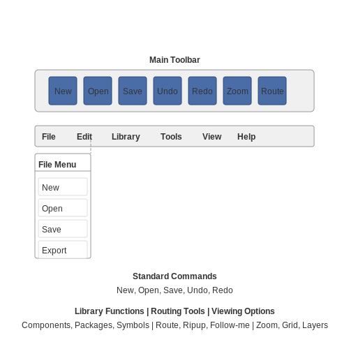
2.2 Design Workspace Layout
Designing a PCB layout in Eagle CAD requires not only familiarity with the software's tools but also an understanding of how to effectively arrange the workspace for optimal workflow.
Understanding the Workspace Environment
Eagle CAD provides a flexible and user-friendly environment tailored for PCB design. The primary interface consists of several key components:
- Toolbars: These provide quick access to basic tools such as drawing lines, placing components, and routing connections.
- Layers Panel: Here, different layers of your circuit design can be managed, including copper layers, silkscreen, and solder masks.
- Design Rule Check (DRC): This function allows you to establish and review your design constraints, ensuring your layout adheres to manufacturing standards.
A well-organized layout within these components can significantly enhance efficiency during the design process. The layout's configuration directly affects how intuitively you can interact with the information on your screen, which is crucial in complex designs.
Customizing Your Workspace
To maximize productivity, customizing the workspace layout is essential. Here are some practical strategies to enhance workspace efficiency:
- Using Multiple Monitors: If possible, spread the workspace over multiple screens. For instance, use one monitor for schematics and another for board layout.
- Organizing Toolbars: Tailor the toolbars to include only the tools you frequently use. To do this, right-click on the toolbar area and select the options to add or remove tools. This minimizes distraction and focuses your attention on the essential functions.
- Layer Management: Make sure the layers panel reflects the components relevant to the current tasks. For instance, hide layers that are not currently being edited to reduce on-screen clutter.
By adopting these practices, you can create a workspace that not only accommodates your design aesthetic but also streamlines your workflow, which is particularly important when working on intricate layouts with numerous components.
Real-World Application: Case Study
An illustrative example of efficient workspace layout can be seen in the design of high-frequency PCB circuits. In such applications, managing layer stacks and understanding the electromagnetic interference (EMI) principles are vital. An effectively laid out workspace allows engineers to visualize how signals propagate through the board and quickly access simulation tools to test their designs.
Furthermore, routinely using design rule checks within Eagle CAD ensures that your layout adheres to constraints, potentially saving time and costs associated with manufacturing errors.
Conclusion
In conclusion, a carefully arranged design workspace layout in Eagle CAD is pivotal to enhancing productivity, particularly for advanced users working on complex PCB projects. Implementing these strategies can lead to significant improvements in your design cycle efficiency, ultimately contributing to the successful realization of your engineering projects.
2.3 Navigating the UI
In mastering Eagle CAD, a powerful PCB design tool, understanding its user interface (UI) is critical for enhancing productivity and ensuring precision in your electronic designs. The UI encompasses various panels, menus, and toolbars that aid in project navigation, component placement, and schematic design management. This subsection will delve into the essential components of the Eagle CAD interface and provide insights into optimizing your workflow in this environment.
Understanding the Layout
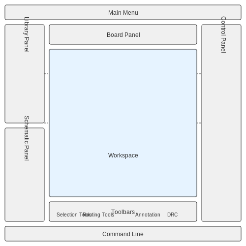
The Eagle CAD UI is organized into several key components:
- Main Menu: This horizontal bar at the top contains menus such as File, Edit, and Tools, allowing access to various functionalities.
- Control Panel: Located on the right side, it provides quick access to libraries, components, and design rules applicable to your project.
- Command Line: Situated at the bottom, this allows for entering commands directly, improving efficiency for advanced users.
- Workspace: The central area where you create your schematic and board layouts. It supports zooming and panning for detailed work.
By familiarizing yourself with these sections, you will enhance your navigation efficiency, allowing for a more seamless design experience. For instance, using keyboard shortcuts found in the main menu can significantly speed up your workflow, enabling quick access to common functions and commands.
Panels and Their Functionality
The UI is also equipped with various panels that can be shown or hidden based on your needs. Among these:
- Library Panel: This panel is crucial for component selection. It enables you to browse available libraries and add components to your design.
- schematic Panel: Displays your schematic as a circuit diagram and allows for real-time edits.
- Board Panel: This represents the PCB layout, where routing and placement of components occur.
To optimize your Eagle CAD experience further, consider customizing the UI according to your preferences. This includes rearranging panels, saving workspace configurations, and adjusting settings to suit your project requirements. For example, a common approach is to have the library panel readily accessible on the workspace to facilitate easier component selection during design.
Using Toolbars Effectively
Eagle CAD features several toolbars that provide quick icons for frequently used tools. These include:
- Selection Tools: Enable you to select, move, and modify components within your schematic or layout.
- Routing Tools: Assist with the physical layout of traces on the PCB. Familiarizing yourself with these can drastically improve layout efficiency.
- Annotation and Design Rule Check (DRC): These tools ensure adherence to design specifications, minimizing errors in your PCB productions.
For advanced users, mastering the art of layer management and effective use of the toolbar will illuminate how different elements interact within your designs, providing insights into optimizing performance and reliability in the final product.
Conclusion
Understanding and navigating the Eagle CAD UI is not just about familiarity; it enhances your capability to design intricate PCBs efficiently and effectively. Advanced users leverage the UI’s functionalities to optimize performance and streamline their design workflow. As you become more proficient with these tools and features, you will find your design process becoming faster and more intuitive, enabling you to focus on the engineering behind your projects.
In the next section, we will delve into the library management features in Eagle CAD, which are critical for sourcing and managing components efficiently.
3. Starting a New Project
3.1 Starting a New Project
In the domain of electronic design automation (EDA), mastering a tool like Eagle CAD is pivotal for engineers and researchers looking to materialize their ideas into functional circuit boards. Starting a new project effectively sets the stage for successful circuit design, allowing for efficient organization and streamlined workflows. In this section, we will delve into the crucial initial steps for initiating a new project in Eagle CAD, covering essential features, file structures, and preliminary setups.
Understanding the Project Framework
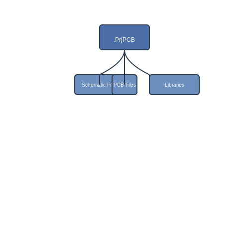
Before we dive into the practical steps, it's important to recognize the framework underpinning a project in Eagle CAD. Each project generally comprises various elements including schematic files, board layout files, and libraries. These components are housed within a project folder, providing a structured environment for your designs. This organization is critical, especially when working on complex designs or collaborating in team settings.
Launching Eagle CAD
To start a new project, your first step is to launch Eagle CAD. If you have not installed it yet, ensure to download and install the suitable version from the official website. Once the software is open, you will encounter the welcome screen, which provides various options to create new projects or open existing ones.
Creating a New Project
To create a new project, navigate to the Control Panel. Here, follow the subsequent steps:
- Right-click on the projects folder or any existing project folder where you want to add the new project.
- Select New Project from the context menu. This action will create a new project directory.
- Rename the project folder to a meaningful title that reflects the design you'll be working on—such as "Power Supply Design" or "RF Amplifier Prototype".
Setting Up the Project Files
Once your project folder is created, you need to add schematic and board files, which are essential for your design workflow.
- To add a schematic, right-click on the project folder and choose New > Schematic. This will open a new schematic workspace.
- For adding a PCB layout, right-click again on the project folder and select New > Board. This allows you to design your PCB layout based on your schematic.
This separation of schematic and board files is significant as it enables you to work iteratively. You can easily update the schematic, and these changes will be reflected in the board layout, ensuring both designs are in sync.
Organizing Libraries and Components
Eagle CAD projects typically utilize various components from libraries. To ensure that your design operates smoothly, it is vital to consolidate your component libraries within the project structure:
- Navigate to the Library icon in the Control Panel, where you'll find default libraries available online.
- For custom parts, you may want to create or import your library files into the project. This is essential if you are using specific components not found in the default libraries.
Conclusion and Practical Considerations
With your Eagle CAD project set up, you are now prepared to embark on the design process. Remember, an organized structure not only simplifies your workflow but also plays a pivotal role in collaboration with fellow engineers and researchers. A well-prepared project can significantly reduce the risk of errors and ensure a smooth development cycle moving forward.
3.2 Schematic Design Basics
The process of schematic design serves as the foundation for any electronic project, acting as a blueprint from which all subsequent circuit development flows. In Eagle CAD, mastering the principles of schematic design is not just beneficial—it’s essential for enhancing design accuracy, reducing errors, and facilitating the eventual translation from concept to physical reality.
Understanding the Schematic Layout
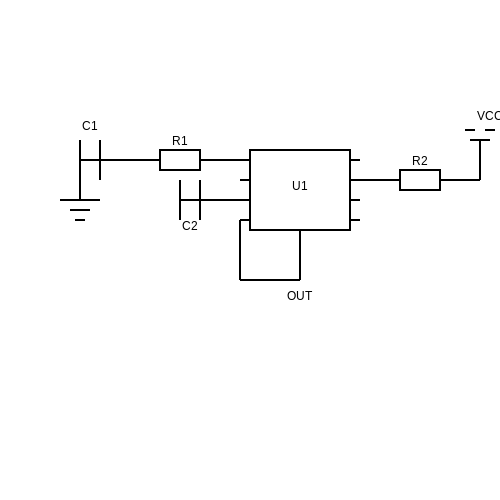
A schematic diagram represents the functional connections between various components in a circuit. This visual representation is composed of symbols, lines, and notations that convey information about the electrical characteristics and relationships of the components. Key elements within a schematic include:
- Component Symbols: Unique graphical representations for resistors, capacitors, integrated circuits, and other electronic devices.
- Wiring Connections: Lines that connect these symbols, indicating how electricity will flow through the circuit.
- Annotations: These include part values, component designators (e.g., R1, C2), and functional notes that assist in understanding the overall design.
Creating a New Schematic in Eagle CAD
To begin a new design in Eagle CAD, initiate the software and select the appropriate option to create a new project. Within the project, you can add a new schematic, which opens a blank canvas for your designs. The following steps outline the initial setup for your schematic:
- Select Components: Utilize the library manager to find and add components that you wish to use in your design. Eagle CAD comes with an extensive library, but you can also create custom components if needed.
- Place Components: Drag and drop components onto the schematic workspace. Ensure that they are placed logically, as this will make the wiring and troubleshooting process much easier.
- Connect Components: Use the wire tool to create connections between components. Pay close attention to junctions and ensure that connections follow conventional schematic practices.
Utilizing Layers for Clarity
Eagle CAD operates on a layered approach, allowing you to separate different types of information on the same schematic. For instance, you can use one layer for the component layout and another for annotations. This is particularly useful when dealing with complex systems, as it can help in minimizing clutter and improving readability.
Rules for Effective Schematic Design
To ensure that your schematic is effective and reduces the risk of errors during the physical prototype phase, consider the following guidelines:
- Keep it Organized: Group related components together and use hierarchical designs when applicable to enhance readability.
- Label Correctly: Use clear and consistent labeling for all components and connections, making it easier for others to understand your design.
- Review Electrical Rules: Eagle CAD includes features that enable you to check for common electrical rule violations, such as unconnected pins or excessive voltage drops.
Practical Applications
Mastering the basics of schematic design in Eagle CAD can have profound implications in the real world. For instance, engineers might employ these skills in designing critical systems for aerospace applications or medical devices, where high reliability is paramount. A meticulously crafted schematic can serve as a fundamental document for further processes such as simulation, PCB layout, and eventual manufacturing.
The essence of successful schematic design lies in its ability to effectively communicate intentions and functionality, establishing a clear path from concept to physical implementation.
3.3 Creating Board Layout from Schematic
In the process of designing printed circuit boards (PCBs), transitioning seamlessly from a schematic to a board layout is crucial. Eagle CAD offers a robust environment for accomplishing this task, enabling engineers to create sophisticated designs efficiently. This section focuses on the intricate steps involved in generating a board layout from a schematic, peppered with practical applications to illuminate its relevance in real-world scenarios. Understanding the basic principles of schematic design is imperative. A schematic captures the relationships between components in an electronic circuit, incorporating symbols and interconnections. In Eagle CAD, once the schematic design is satisfactorily completed and error-checked, the next step is to create the physical layout that will facilitate the assembly and functioning of the electronic device.3.3.1 Transferring Schematic to Board Layout
To transfer the schematic to the board layout in Eagle CAD, one begins by selecting the "Switch to Board" option. This action generates an initial board layout based on the schematic components. If no board exists, Eagle CAD prompts users to create a new board file. This new board file incorporates all components from the schematic but without any defined footprints or placements. Once the board layout opens, users will generally see an empty workspace where components need to be placed strategically. At this juncture, it's essential to consider factors such as the physical size of the PCB, component spacing, and the arrangement that best minimizes trace lengths while optimizing signal integrity.3.3.2 Defining Board Size and Shape
Before placing components, one must outline the PCB's dimensions. Setting a suitable board outline is paramount. Users typically employ the "Dimension Layer" to delineate the board edges accurately. In this layer, users can sketch the desired shape, which will serve as the boundary for all components and traces. For instance, a rectangular board might be suitable for modular designs, while custom shapes might be necessary for compact or ergonomic devices. After creating the outline, it's critical to include cutouts for mounting holes or connectors, which enhances functionality and manufacturability.3.3.3 Component Placement Strategies
Placement of components is both an art and a science, necessitating an understanding of electrical principles alongside practical design considerations. During this phase, several strategies can be employed: 1. Group Related Components: Placing components that are functionally related in proximity can reduce trace lengths, which is pivotal for minimizing parasitic capacitance and inductance. 2. Follow Layout Guidelines: Utilize guidelines and best practices tailored for specific applications, including high-frequency circuits, where trace lengths and impedance control are critical. 3. Trial and Error: Employing an iterative approach that allows for adjustments can be invaluable. Initial placements can be fine-tuned based on simulation results or prototype testing feedback. Once components are placed, a thorough review of spacing and alignment should be conducted to ensure compliance with manufacturing tolerances and design rules.3.3.4 Routing the PCB
After components are strategically placed, routing the PCB begins. This step involves connecting components through traces—linear paths on the board. Eagle CAD automates parts of this process, but manual routing often improves design quality and efficiency. The design rule check (DRC) features within Eagle CAD ensure that traces maintain the correct width and spacing, given the current carrying requirements and capabilities of the PCB's substrate material. Adhering to these guidelines helps avoid potential issues like thermal failures and signal integrity problems. Routing involves selecting appropriate trace widths and using vias to connect different layers if a multilayer PCB is needed. Engineers should also be mindful of ground copper areas to minimize return path inductance, which is particularly critical in high-speed applications.3.3.5 Finalizing the Board Layout
Once the routing is complete, and layout checks confirm compliance with design rules, the board is nearing finalization. Additional steps often involve checking the footprints for each component, optimizing the placement of vias, and revisiting specific traces for improvements before preparing for fabrication. At this phase, generating output files for manufacturing becomes essential. In Eagle CAD, users can create Gerber files required for PCB fabrication, along with assembly drawings which stipulate component placements for assemblers. In summary, creating a board layout from a schematic in Eagle CAD is an iterative process that hinges on rigorous understanding and application of both theoretical and practical elements of electronics design. From defining board outlines to executing precise routing, each step builds upon the last, leading to a polished and functional PCB ready for production and implementation in electronic devices. In the next section, we will delve further into the post-layout processes including simulation and testing to ensure robust performance of final designs.4. Using the Component Library
4.1 Using the Component Library
In the realm of electronic design automation (EDA), the ability to efficiently navigate and utilize component libraries is essential for the development of effective schematic and PCB layouts. Eagle CAD, a widely used EDA software, provides a comprehensive component library that facilitates users in selecting and integrating components into their designs. This section delves into the intricacies of using the component library in Eagle CAD, enabling advanced users to enhance their design workflows and optimize performance.
Understanding the Component Library Structure
Eagle CAD’s component library consists of schematic symbols, package footprints, and simulation models. The systematic organization of these elements allows users to seamlessly access a variety of components, from resistors and capacitors to integrated circuits (ICs) and custom parts. Typically, the library is categorized in folders within the software interface, which can be explored to find components based on their specific properties or functions.
Each library element is characterized by:
- Symbol: Represents the component in the schematic diagram.
- Package: Defines the physical footprint required for PCB layout.
- Technology: May include additional information necessary for simulating circuit behavior.
Accessing and Navigating the Library
To access the component library, users can utilize the Library menu in Eagle CAD. Within this menu, users have the option to:
- Open Library: Load predefined libraries that come with Eagle CAD or user-customized libraries.
- Add Library: Include third-party libraries or personal libraries that may contain specialized components not available in the default list.
For effective navigation, users can utilize the library browser that offers search functionality based on component names or attributes. The search feature proves invaluable when dealing with extensive libraries. For example, querying “Op-Amp” can quickly filter and retrieve relevant components, thus streamlining the design process.
Incorporating Components into Your Design
Once the desired component is located, users can incorporate it into their schematic by employing the drag-and-drop functionality. Alternatively, the component can be placed by double-clicking on it within the library browser. In advanced usage scenarios, creating custom components may be necessary. This involves:
- Defining the component’s schematic symbol in the library editor.
- Assigning a PCB footprint to correspond with manufacturing requirements.
- Including any necessary simulation models for circuit analysis.
This flexibility allows engineers and researchers to adapt design tools to their specific parameters, enhancing the applicability of their designs in real-world applications.
Library Management and Customization
Efficient management of component libraries is crucial, especially when dealing with multiple projects. Eagle CAD allows for:
- Creating Custom Libraries: Users can curate materials tailored to their specific design needs, incorporating frequently used components.
- Library Maintenance: Regularly updating libraries ensures that users have the latest components and optimizations for performance improvements.
Moreover, understanding the intricacies of library management can lead to enhanced productivity. With a well-organized library tailored to specific projects, design time can be significantly reduced.
Real-World Applications
The practical relevance of a well-structured component library is exemplified by its application in complex systems design such as embedded systems, telecommunications, or defense electronics. For instance, in designing a compact communication module, engineers can leverage library components to optimize space on PCBs without sacrificing functionality.
In conclusion, mastering the component library in Eagle CAD is fundamental for advanced-level users aiming to push the boundaries of electronic design. By harnessing the tools available within the software, such as component searches, customized library creation, and effective integration methods, engineers can significantly enhance their design capabilities and innovate within their fields.
4.2 Creating and Managing Custom Parts
In the realm of PCB design, particularly when using Eagle CAD, the ability to create and manage custom parts is indispensable. This section delves into the advanced processes of custom component creation and management, a skill often required for engineers seeking to tailor their designs to specific needs or to integrate unique functionalities into their circuits.Understanding Custom Parts
Custom parts refer to PCB components that are not available in standard libraries. They might include specialized microcontrollers, unique sensors, or even bespoke connectors. Utilizing custom parts allows engineers to push the boundaries of creativity and engineering, crafting solutions that are finely tuned to a project’s specifications. The custom creation process typically involves defining the component's electrical, graphical, and mechanical character. By mastering these elements, engineers can ensure perfect integration into their projects.Beginning the Creation Process
To create a custom part in Eagle, the process begins in the schematic editor. You need to define the new component that will later be integrated into the PCB layout. Here are the crucial steps involved: 1. Accessing the Library Editor: The library editor is your primary workspace for creating custom components. Open it by selecting `File > New > Library` from the main menu. This action creates a new library file where all custom parts will be stored. 2. Creating a New Device: Under the library editor, you will define your custom part as a new device. Navigate to `Library > New Device`, and a window will pop up prompting you to enter a device name and set its parameters. This setup allows for organization and easy identification later. 3. Defining the Symbol, Package, and Device: - Symbol: The visual representation of the component in the schematic. Use the `Symbol` editor to design your symbol, focusing on making it intuitive and recognizable. - Package: The physical footprint of the component on the PCB. This part is crucial, as it governs electrical and mechanical fitting. Utilize the `Package` editor to design the footprint that will accommodate your part. - Device: This is the combination of the symbol and the package. In the `Device` editor, link the symbol and package together, defining pins accordingly. Each pin must align perfectly with physical connections to function as intended. 4. Pin Configuration: It is vital to define the pin configuration accurately as this dictates how your new component will interface with others in the circuit. Pay special attention to naming conventions and designating the correct functions. 5. Save and Test the Library: After creating the device, save your library. You can test it by adding your custom part to a schematic to ensure it behaves as expected. Verifying functionality at this stage can save significant time and effort later in the design process.Managing Custom Parts
Once you have created custom parts, managing them effectively becomes critical, especially as projects scale. Here are several best practices: - Organize Libraries Methodically: As your library grows, intuitive categorization is key. Group components based on project types, frequency of use, or manufacturer. This organization enhances accessibility and efficiency during design. - Version Control: Always maintain version control for custom components. Noting changes helps to ensure reliability, especially when collaborating in teams or when returning to a project after some time. - Documentation: Keep detailed documentation of custom parts that includes usage notes, pin configurations, and fabrication requirements. This repository aids in both current and future projects. - Regular Updates: As new components become available or as specifications change, regularly review and update your custom parts library to keep up with technological advancements and project requirements.Real-World Applications
Custom parts are vital in various applications, ranging from aerospace engineering to consumer electronics. For instance, in the development of a unique sensor array for environmental monitoring, engineers often need to create custom parts that can integrate seamlessly with existing technologies. The ability to tailor components can facilitate innovations that lead to advancements in efficiency, miniaturization, and cost-effectiveness. By mastering the creation and management of custom parts in Eagle CAD, engineers can enhance their capabilities, unlocking new potential for their designs. This skill not only supports individual projects but also contributes to broader advancements in engineering practice and technology development.Conclusion
The ability to create and manage custom parts in Eagle CAD is an advanced skill essential for engineers and designers looking to innovate. Through understanding component representation, library structure, and effective management practices, you can significantly enhance your design workflow, ensuring alignment with project specifications and fostering creative engineering solutions.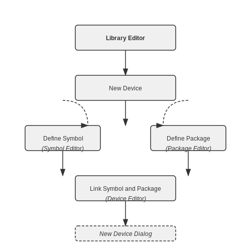
4.3 Importing External Libraries
As a powerful PCB design tool, Eagle CAD provides a wealth of features that can greatly enhance the design process. One such feature is the ability to import external libraries, which is vital for integrating custom components that are not included in the standard libraries. This section explores the entire process, from understanding what an external library is to practical steps for efficient utilization within Eagle CAD.
Understanding External Libraries
In the context of PCB design, an external library refers to a collection of components, footprints, and symbols that can be used in your design projects. Unlike the built-in libraries that come with Eagle CAD, external libraries allow you to add specialized components, such as specific sensors, ICs, or connectors that may not be covered by the default options.
Why Import External Libraries?
The importation of external libraries enhances design flexibility and accuracy. Consider scenarios where:
- Custom Components: You are designing a device using a specific microcontroller or sensor that is not available in Eagle’s built-in libraries.
- Legacy or Unique Designs: You are working on legacy systems or custom equipment that requires unique parts.
- Community Resources: Many community-based libraries contain parts created by other engineers that can expedite your design process.
The ability to import these components efficiently can drastically accelerate your workflow and improve your design outcomes.
Steps to Import External Libraries
To begin importing external libraries into your Eagle CAD workspace, follow these structured steps:
Step 1: Obtain the Library Files
External libraries are generally available in .lbr file format. You can find these files through various online repositories, manufacturer websites, or community forums. Once you have downloaded the appropriate libraries, note their storage location for future reference.
Step 2: Open Your Eagle CAD Project
Launch Eagle CAD and open the project to which you wish to add components from the external library. This project should be initiated and saved as you will be modifying it.
Step 3: Load the Library in Eagle CAD
Navigate to the library manager, typically found under the Libraries section. Here, you can manage both built-in and external libraries. Select the option to 'Add' or 'Load' a library, then navigate to the location of your downloaded .lbr file. Once located, select the file and add it to the active libraries list.
Step 4: Verify and Use Components
After successfully importing the library, verify that the components are accessible from the components tool. To do this, invoke the part placement dialog, allowing you to browse through the newly added library. You can then select your desired components to integrate them into your design.
Common Challenges and Troubleshooting
Occasionally, importing libraries may not be straightforward. Here are some common issues and their solutions:
- Library Not Displaying: Ensure the library file is compatible with your version of Eagle CAD. If not, you may need to convert it or find a suitable version.
- Missing Footprints: Sometimes components may not have associated footprints. You may need to create or locate these separately to use the components effectively.
- Corrupted Files: If you encounter errors during loading, check the integrity of the library file or consult community forums for alternatives.
By mastering the importation of external libraries, you empower yourself to customize your PCB designs effectively, enhancing both functionality and innovation in your projects.
5. Setting Design Rules
5.1 Setting Design Rules
In the realm of PCB design, particularly when using Eagle CAD, establishing coherent and robust design rules is a fundamental step towards ensuring both functionality and manufacturability of your circuits. Design rules dictate the acceptable parameters for your layout, influencing factors such as track width, spacing, and layer stack-up. Properly defining these rules not only enhances the reliability of the final product but also streamlines the design process, minimizing the risk of errors during manufacturing.
Understanding Design Rules
Design rules in Eagle CAD are essentially constraints or guidelines that dictate how components are arranged and interconnected on the printed circuit board (PCB). These rules can be set to cover various aspects:
- Electrical Clearance: This defines the minimum distance between conductive elements to avoid short circuits.
- Trace Widths: The width of traces must be chosen based on current-carrying requirements, which directly influences the thermal and electrical performance of the PCB.
- Routing Environments: Rules can also dictate the allowable area for routing traces between components.
By applying these rules, you ensure that the PCB can be manufactured reliably and operates correctly under specified conditions. Moreover, it is crucial to understand that different components and technologies may require adjustments to these standard design rules. As technology advances with smaller components and higher speeds, the importance of diligently setting design rules becomes even more pronounced.
Setting Design Rules in Eagle CAD
To set design rules in Eagle CAD appropriately, follow these steps:
- Open the Design Rules Dialog: Navigate to the Tools menu and select Design Rules. This will bring up a dialog box where you can set all relevant parameters.
- Define Electrical Rules: Under the Electrical tab, you can specify distances between pins, traces, and other conductive elements. Make sure to adjust the Clearance, Distance, and Width accordingly, based on your specific component specifications. Use the Current Capability to guide your trace widths.
- Set Manufacturing Rules: In the Manufacturing tab, you can specify rules that pertain to the manufacturing process, such as dimensions for holes and board outlines. It’s beneficial to consult your PCB manufacturer for their specific requirements.
- Layer Setup: Use the Layers tab to designate the different layers of your PCB, providing flexibility based on the complexity of your design.
Each of these design rules must be meticulously documented and understood to avoid potential manufacturing delays and functional failures. As many PCB designs make use of rapid prototyping features enabled by Eagle CAD, keeping these rules consistent ensures one can achieve optimal results across iterations.
Real-World Applications and Case Studies
The importance of robust design rules cannot be overstated in real-world applications. Consider the aerospace sector, where a failure in PCB design can lead to catastrophic results due to high-stakes operational environments. Engineers have found that enforcing stringent clearance and trace width rules leads to increased reliability in high-frequency applications, enabling designs suitable for RF and microwave circuits.
Furthermore, in consumer electronics, maintaining uniformity in design rules across various product lines can significantly reduce production costs and time-to-market. For example, companies frequently leverage Eagle CAD's design rule checks (DRC) to ensure compliance before proceeding to manufacturing, thus reducing the likelihood of costly redesigns.
As you set out to establish design rules, always consider the engineering principles and practical needs behind each criterion, and stay informed about current trends and standards within the industry.
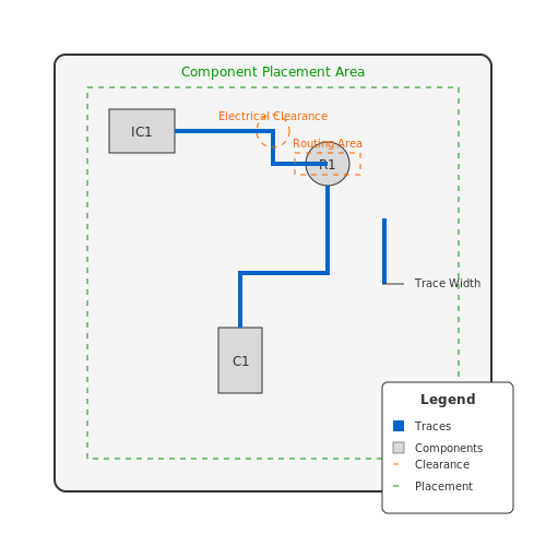
5.2 Running DRC Checks
In the world of PCB design, ensuring the correctness of your layout is paramount. One of the most effective ways to achieve this is by running Design Rule Checks (DRC). This process identifies violations of design rules, thereby preventing potential manufacturing issues that could arise from shorts, opens, or other layout errors. In Eagle CAD, DRC is a powerful tool that engineers can leverage to validate the integrity of their designs.
Before diving into the specifics of running DRC checks in Eagle CAD, it is essential to appreciate the significance of design rules. Design rules are a set of parameters that define the layout constraints for components and traces, influencing factors such as trace width, spacing between traces, and pad sizes. These rules are dictated by the manufacturing capabilities of PCB fabricators, ensuring that designs are not only functional but also manufacturable.
Setting Up Design Rules in Eagle CAD
Eagle CAD allows users to specify various design rules tailored to particular manufacturing processes. To configure these rules, follow these steps:
- Open your project in Eagle CAD.
- Navigate to the DRC option under the Tools menu.
- In the DRC window, you will find several options, such as Clearance, Width, and Size. Customize these fields based on your PCB fabricator's specifications.
- Once you have defined your rules, click to save your settings.
This step ensures that every subsequent design review takes into account the limitations and capabilities of the manufacturing process you intend to use.
Running the DRC
Once you have configured your design rules, the next step is to execute the DRC process. This can be initiated from the same DRC menu you accessed earlier. Here’s how:
- With your layout open, go back to the Tools menu and select DRC.
- Click on the Run button in the DRC dialog.
The DRC engine will analyze your board against the outlined design rules, providing feedback in the form of error markers displayed on the schematic or board layout. Each marker represents a violation of the specified rules and will often include a description detailing the nature of the issue.
Analyzing DRC Results
Upon completing the DRC check, carefully review the markers on your board. Each one requires your attention. Typically, you may encounter the following common types of violations:
- Clearance Issues: This occurs when components or traces are too close together. Modify your layout to ensure sufficient spacing.
- Width Violations: This indicates that a trace is thinner than specified. Widen the trace to comply with the design rules.
- Pad Size Errors: If a pad is not the correct size for its associated component, it may lead to soldering issues upon manufacturing. Adjust the pad size accordingly.
It is prudent to resolve these violations methodically, as neglecting to address them can lead to costly revisions during the manufacturing process.
Real-world Application and Practical Relevance
Many engineers utilize DRC as a crucial step in their PCB design workflow. For instance, in the development of consumer electronics where cost and reliability are critical, running DRC checks not only aids in saving time but also decreases the likelihood of assembly failures. Summarily, an efficient DRC process translates to improved product quality, reduced time to market, and decreased waste – factors that are invaluable in today’s competitive landscape.
In conclusion, DRC checks within Eagle CAD serve as a robust mechanism for ensuring that PCB designs comply with essential manufacturing requirements. By understanding and effectively implementing DRC in your workflow, you can significantly enhance the quality and reliability of your electronic designs.
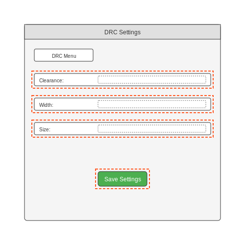
5.3 Interpreting DRC Errors
Design Rule Check (DRC) is an essential component of PCB design in Eagle CAD. It evaluates whether the layout adheres to specified design rules that ensure proper functionality and manufacturability. Understanding how to interpret DRC errors is vital for advanced users in ensuring a clean and effective design.
Understanding DRC Errors
When you run a DRC in Eagle CAD, the software scans the entire layout based on predefined rules related to spacing, widths, and certain geometrical constraints. It flags violations known as DRC errors. Each error corresponds to specific elements in your design and requires your attention. These elements can include:
- Wire spacing: This error occurs when two wires (or traces) are too close to each other, which could lead to crosstalk or shorts.
- Pad size: If the pads are smaller than recommended, there may not be adequate room for solder to adhere, potentially leading to weak joints.
- Route width: A trace that is too thin may not carry the required current, risking overheating and failure.
- Component clearance: Errors occur when components are placed too close to each other or to edges, which can hinder assembly and performance.
Practical Relevance of DRC Errors
Addressing DRC errors is not merely about fixing the visible issues; it has profound impacts on device reliability and performance. In critical applications like aerospace and medical devices, neglecting certain rules may result in catastrophic failures. Besides, certain errors can lead to costly re-spins of PCB designs. An effective approach involves frequent checks during the design process rather than running a final check before fabrication.
Interpreting Error Messages
Eagle CAD provides error messages that can initially seem cryptic. They often reference specific components, layers, or gaps rather than simply listing the nature of the error. Let’s go over how to effectively interpret these messages:
- Error Location: The DRC will highlight the areas in the layout where violations occur. Clicking on the error in the report will direct you to the problematic area, allowing for quick identification.
- Error Type: Each message contains error codes that correspond to specific rule violations. Familiarizing oneself with these codes can greatly reduce the time taken to rectify issues.
- Simplifying Rules: Users have the option to customize design rule parameters based on their specific applications, making it vital to understand how these affect error generation.
Case Study: DRC Error Resolution
Consider a hypothetical example where a user receives a warning for insufficient wire spacing in a high-frequency circuit. The user may elect to either widen the trace or redistribute the layout to maintain performance while adhering to design rules. Iterative adjustments followed by successive DRC checks allow for a streamlined resolution process.
In conclusion, interpreting DRC errors in Eagle CAD is a crucial skill for seasoned designers. It is not just a matter of rectifying issues; it embodies a holistic approach to ensuring optimum performance, reliability, and manufacturability in designs. Comprehensive understanding and frequent checks can significantly enhance the professionalism of the design process.
6. Generating Gerber Files
6.1 Generating Gerber Files
In the context of PCB design, Gerber files play a crucial role in manufacturing by serving as the standard format for representing the printed circuit board's layers and features. When using Eagle CAD for designing PCBs, generating Gerber files is a vital step that allows designers to convey detailed manufacturing instructions to fabrication plants. When you finalize your PCB design in Eagle CAD, the process of generating Gerber files involves extracting data from your layout, including the copper layers, silkscreen, and solder mask, and exporting it into a format readable by PCB manufacturers. This section will walk you through the key steps needed to create high-quality Gerber files efficiently.Understanding Gerber File Types
Before diving into the process, it's essential to understand the various types of Gerber files produced during this operation. There are typically several critical layers in a PCB layout:- Top Copper Layer: Represents the copper traces on the upper side of the board.
- Bottom Copper Layer: Represents the copper traces on the lower side.
- Top Silkscreen Layer: Contains text and symbols printed on the top of the PCB.
- Bottom Silkscreen Layer: Contains the same information for the bottom side of the PCB.
- Solder Mask Layers: Files that illustrate the areas where solder mask is applied to prevent solder from bridging between components.
- Drill Files: Details the locations and sizes of holes that will be drilled into the PCB.
Step-by-Step Guide to Generating Gerber Files in Eagle CAD
The following steps will guide you through the process of generating Gerber files in Eagle CAD. Ensure that your design is complete, and you have performed all necessary DRC (Design Rule Check) checks before exporting.Step 1: Prepare Your Board Layout
Before generating Gerber files, double-check your PCB design for potential errors. Utilize Eagle CAD’s DRC tools to validate your layout against defined standards. A well-prepared board ensures the associated Gerber files will be accurate and reflect your intentions.Step 2: Accessing the CAM Processor
To generate Gerber files, navigate to the CAM processor:- In Eagle CAD, select the 'File' menu.
- Click on 'CAM Processor'.
Step 3: Select and Configure Gerber Job
Eagle CAD typically provides default jobs for generating Gerber files. You will need to select one that suits your design needs:- Choose the job called “Gerber”.
- Review each layer to ensure all necessary elements (as discussed earlier) are included.
Step 4: Open and Adjust Settings
In the job configuration screen:- Use the “Output” section to specify the file destination and names.
- Check the settings for each layer and ensure all relevant ones are selected, including the copper and silkscreen layers.
Step 5: Generate and Save
Once you are satisfied with the settings, click on the “Process Job” button to generate the Gerber files.- The files will be created in the designated output folder.
- Check the output window for any errors. If all goes smoothly, you should receive confirmation of successful file creation.
Post-Processing: Verify the Gerber Files
After generating the Gerber files, it's crucial to verify their accuracy. Use a Gerber viewer software to load the files and inspect the different layers. Proper verification can prevent costly manufacturing errors and provide assurance that your design will work as intended in practice.Practical Applications of Gerber Files
The generated Gerber files can be sent directly to PCB manufacturers. With proper design and verification, the resultant PCB can support various applications, from simple hobbyist projects to complex commercial products. For an engineer or researcher, mastering the nuances of generating accurate Gerber files using Eagle CAD is not only fundamental but also a key to streamlining the development process and ensuring high-quality production outcomes for electronic devices.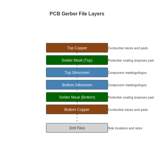
6.2 Exporting Bill of Materials (BOM)
In the realm of PCB design, the Bill of Materials (BOM) serves as a cornerstone document, encapsulating essential information about the components needed for assembly. Eagle CAD, a popular PCB design software, facilitates the generation and export of BOMs that can be utilized for manufacturing, procurement, and project management. Understanding how to effectively export your BOM is critical for engineers and designers striving for efficiency and accuracy in their projects.
Understanding the Importance of a BOM
A well-structured BOM is crucial for both communication and organization in engineering projects. It lists all required components, including part numbers, quantities, values, and footprints, ensuring that every team member is aligned on component specifications. When exporting a BOM from Eagle CAD, one can create formats suitable for different applications, such as Excel spreadsheets or XML files, which can seamlessly integrate into various manufacturing processes and ERP systems.
Steps to Exporting a BOM from Eagle CAD
Exporting the BOM in Eagle CAD consists of a few systematic steps that transform your schematic and layout data into a usable format. The following procedure outlines the process:
- Open Your Project: Launch Eagle CAD and open the project containing the schematic and PCB layout from which you wish to export the BOM.
- Navigate to the BOM Tool: Go to the “Tools” menu located in the top toolbar, then select “BOM.” This action opens the BOM configuration window.
- Configure BOM Settings: In the BOM window, you can customize which components are included in the BOM. This includes filtering options to select specific parts based on attributes such as value or package type. You can also set the desired output format.
- Generate the BOM: After configuration, click the “Generate” button. Eagle CAD processes the existing components in your schematic and layout to compile the BOM based on your settings.
- Export the BOM: Finally, you can export the generated BOM into your chosen format. Select the desired output option, such as CSV, TXT, or XML. Specify a location on your computer to save the file, and confirm the export.
Customization Options for Effective BOM Management
The customization options available during the BOM export can significantly enhance its effectiveness. For instance, you can choose to include or exclude certain attributes, such as supplier information or component descriptions. This level of customization allows you to tailor your BOM according to the requirements specified by your manufacturing partner or project documentation.
Real-World Applications and Case Studies
One practical application of exporting BOMs arises in the context of collaborative projects involving multiple stakeholders, such as design engineers, procurement specialists, and manufacturers. A well-prepared BOM enables efficient communication across these groups, reducing the chances of discrepancies and facilitating smoother transitions from design to production.
For example, consider a case where a startup company is developing a novel IoT device. By exporting a clear and comprehensive BOM using Eagle CAD, they can swiftly provide manufacturers with the necessary components list, ensuring timely production and successful project implementation. Moreover, incorporating vendor details within the BOM allows for immediate sourcing, thereby accelerating the procurement process.
In conclusion, effectively exporting and managing a BOM through Eagle CAD not only boosts the efficiency of your PCB design workflow but also enhances collaboration among team members, leading to successful project outcomes.
6.3 Preparing Files for Fabrication
In the realm of PCB development, converting your Eagle CAD design into a manufacturable file is a pivotal step that bridges the gap between digital design and physical product realization. Understanding how to effectively prepare your files not only ensures manufacturing accuracy but also enhances overall production efficiency. This section delves into the various stages of file preparation, focusing on the essential outputs and best practices for sending your designs to fabrication.Exporting Gerber Files
Gerber files are the standard format used in PCB manufacturing, capturing necessary details about the layout, including copper traces, pads, and other features. Eagle CAD proficiently facilitates the generation of these files through its built-in Gerber Export feature. To initiate this process: 1. Navigate to the File menu and select CAM Processor. 2. In the CAM Processor window, load the appropriate job specific to your board design. Eagle provides a number of predefined jobs suitable for various fabrication needs. 3. Review and ensure that the layers you wish to include in the output are properly selected. Common layers include: - Top and bottom copper layers - Silk screen layers - Mask layers - Drill layer Once you have confirmed your selections, you can proceed to export the files: - Click on Process Job to create the Gerber files. Eagle will generate a series of files, usually in the *.gbr format, corresponding to your selected layers. Consider including a comprehensive documentation—often termed as a fabrication drawing or technical data sheet—which details the material specifications, layer stack-up, and any finishing treatments required. This documentation is invaluable for manufacturers as it ensures alignment with your design intentions.Generating Drill Files
In conjunction with Gerber files, generating drill files is essential for the accurate placement of vias and mounting holes on your PCB layout. The Excellon drill file format is commonly used for this purpose. To create drill files in Eagle: 1. Within the CAM Processor, load the appropriate Excellon job file. 2. Confirm the settings, such as the drill sizes and units (imperial or metric), so they align with your PCB design requirements. 3. Proceed to initiate the process, which will yield *.drl files. These drill files should be reviewed in conjunction with your Gerber outputs to verify alignment, as incorrect drill placements can lead to comprehensive manufacturing setbacks.Verification and Validation
Upon completion of file generation, it is essential to conduct validation checks using viewer software to inspect the Gerber layers and drill files. This step is crucial to identify any discrepancies that could arise during manufacturing. Utilize tools such as Gerber viewers or CAM tools to ensure the accuracy of your files. Remember to check for: - Correct alignment of pads and traces - No overlapping or missing features - Proper scaling and dimensions Performing a thorough verification processes increases the chances of a successful fabrication run, saving both time and capital.Submitting Your Files
Once your files are verified, the final step is to package them appropriately before submission to your chosen PCB manufacturer. Ensure you include: - All relevant Gerber files - Drill files - Fabrication prints or design documents - A Bill of Materials (BOM) that outlines component specifications and quantities. Different manufacturing services may require different formats or additional documentation. Therefore, reviewing the guidelines of your PCB manufacturer will help in avoiding unnecessary reworks and delays. Through this meticulous preparation process, you will facilitate a smoother transition from the conceptual phase of design to tangible hardware, thereby enhancing your efficiency as an advanced user of Eagle CAD in PCB fabrication.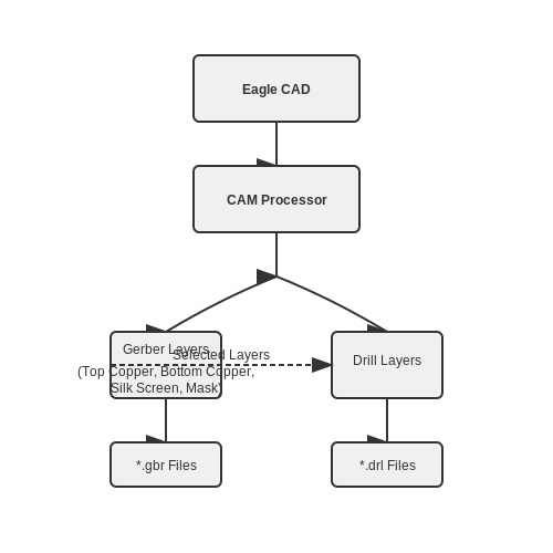
7. Scripting in Eagle CAD
7.1 Scripting in Eagle CAD
Scripting in Eagle CAD unlocks a powerful layer of functionality for advanced users, enabling automation, custom design rules, and enhanced interoperability with various systems. Through the built-in ULP (User Language Program) environment, engineers and designers can create scripts to perform repetitive tasks, generate components, and manipulate designs programmatically. This flexibility can greatly increase efficiency and open new avenues for design innovation.
Understanding ULP: The Foundation of Scripting in Eagle CAD
ULP is a scripting language designed specifically for Eagle CAD. It allows users to tap into the design database of Eagle and manipulate libraries, schematics, and PCB layouts directly. ULP scripts can automate many aspects of the design process, from generating reports to creating complex geometries that would be cumbersome to achieve through manual entry. The core of effective scripting lies in understanding the syntax and core functions within ULP.
Basic Syntax and Structure of ULP
The syntax of ULP is similar to C programming, making it accessible for engineers familiar with programming concepts. A simple ULP script begins with defining the environment and functions. Here’s a breakdown of typical modular components:
- Variable Declarations: You can define variables to store data, such as component attributes or geometric parameters.
- Control Structures: ULP supports conditional statements and loops, thus allowing responses to dynamic conditions during script execution.
- Function Definitions: Functions can encapsulate behavior for reusability, simplifying complex operations within your scripts.
This structure promotes both clarity in design and functionality, enabling quick adaptations in designs as demands change.
Practical Applications: Automation and Customization
Automation through ULP greatly enhances productivity in Eagle CAD. Here are a few key applications:
- Automated Reporting: Generate detailed reports that include component count, net listings, and other essential metrics with a single command.
- Batch Modifications: Update multiple components or attributes across a design, such as changing value specifications or footprint assignments.
- Parametric Generation: Create families of components or layouts based on defined parameters, such as dimensional specifications or material properties.
For instance, consider an example where a script generates a series of resistors with varying values based on user input. A ULP can iterate through a predefined list, creating components in the schematic, ultimately saving hours of manual labor.
Sample ULP Script
string componentName;
int value;
componentName = "R";
for(value = 100; value <= 1000; value += 100) {
    printf("%s%d", componentName, value);
    // Create resistor logic here
}
Advanced Techniques: Debugging and Community Resources
As with any programming language, debugging is a critical skill in scripting with ULP. Utilize the ULP console for error messages and insights into script performance. Each message can guide the user toward identifying problems in logic or syntax.
Furthermore, the Eagle CAD community is a valuable resource. Participating in forums and collaborative projects can lead to discovering pre-existing ULP scripts, innovative practices, and partnerships that push design capabilities further. Building a portfolio of reusable ULP scripts not only enhances personal productivity but also contributes to a culture of sharing knowledge among peers.
In summary, scripting in Eagle CAD through ULP is not merely a technical skill; it is a vital element for innovation and efficiency in electronic design. By mastering ULP, engineers and designers can achieve unprecedented design capabilities and flexibility, thus paving the way for advanced electronic products.
7.2 Using User Language Programs (ULPs)
User Language Programs (ULPs) are an exceptional feature of Eagle CAD, catering to advanced users who wish to enhance their designs through automation and customization. ULPs enable engineers and designers to script functionalities tailored to their workflows, facilitating processes that would otherwise be repetitive or cumbersome.
In this section, we will explore the mechanics of ULPs, including their structure, the scripting language used, and practical applications that highlight their potential in complex design scenarios.
Understanding ULPs
A User Language Program in Eagle CAD is essentially a set of scripts written in a highly-tailored language that is specifically designed to manipulate and interact with Eagle's design database. This allows users to automate tasks such as generating reports, modifying component placements, or automating design rule checks. The ULPs make use of a simplified version of the C programming language, providing a familiar syntax for those with programming experience.
Structure and Syntax
At their core, ULP scripts consist of a sequence of commands that control various aspects of the design environment. The language supports basic programming concepts such as variables, conditionals, and loops, allowing for powerful control flows. Below is a simplified breakdown of the components involved:
- Variables: Used to store data that can be manipulated throughout the script.
- Functions: Encapsulated blocks of code that perform specific actions when called.
- Conditional Statements: Allow code execution based on logical conditions, enhancing decision-making in automation.
- Loops: Repeatedly execute code blocks, which is particularly useful for batch processing in designs.
Creating Your First ULP
To illustrate the utility of ULPs, let’s create a simple script that calculates the total number of components in a design and outputs that information. The following script details this process:
# ULP to count components in the current schematic
int totalComponents = 0;
foreach(component) {
    totalComponents++;
}
printf("Total Components: %d\n", totalComponents);
This script initiates a count of components by iterating through each component in the current schematic. The result is printed to the console, providing a quick overview of the design.
Practical Applications of ULPs
The true power of ULPs becomes evident when considering their application in larger design projects. Engineers can create customized tools for:
- Automated bill of materials (BOM) generation that formats data compatible with procurement systems.
- Design rule checks that validate safety and compliance beyond standard automated checks.
- Batch modifications of library components, ensuring uniformity and efficiency in large projects.
As these examples illustrate, ULPs extend the capabilities of Eagle CAD, making it a robust tool not just for circuit design but also for streamlining workflows in complex engineering projects.
For further exploration of User Language Programs, consider diving into the official Eagle documentation, community forums, or tutorials which focus on advanced scripting techniques to leverage the full potential of this feature.
7.3 Collaborating with Eagle CAD Projects
Collaboration has become an essential aspect of engineering design, particularly in the context of complex electronic systems. Eagle CAD provides a viable environment for multiple users to operate effectively within a single project. This section delves into advanced techniques for collaborating on Eagle CAD projects, emphasizing version control, sharing methods, and efficient teamwork strategies.
Leveraging Version Control Systems
One of the most effective ways to manage collaboration on Eagle CAD projects is through the integration of version control systems (VCS), such as Git. Using VCS allows project teams to track changes, revert to previous states, and manage multiple development branches simultaneously. Typically, engineers can follow these steps:
- Create a Git Repository: Start by initializing a repository for the Eagle project. This can be executed with the command
git initin the project directory. - Commit Changes: Regular commits capture the evolution of the design files. Use meaningful commit messages to describe the changes made.
- Branch Management: Engineers can create branches for features or modifications, ensuring that the main project remains stable during development.
By using Git in conjunction with Eagle, engineers can maintain a clear and organized project structure. This enhances the integrity of designs and minimizes risks associated with untracked changes.
File Sharing Techniques
Effective communication and file sharing are crucial for successful collaboration. Eagle CAD's file management allows users to share designs using several methods:
- Cloud Storage: Utilizing cloud services like Dropbox or Google Drive promotes accessibility, enabling team members to collaborate in real time, regardless of their location.
- Eagle CAD's Project Zip Feature: Eagle allows users to compress the entire project into a single ZIP file. This simplifies file sharing and ensures all necessary components are included.
- Direct Integration with GitHub: For teams using GitHub, integrating Eagle files directly into repositories can streamline workflows. Teams can collaborate on schematic and layout changes efficiently.
In modern engineering practice, ensuring that all team members are synchronized is vital. Adopting these sharing methodologies will significantly enhance collaboration and project outcomes.
Real-World Applications and Case Studies
Collaborative designs in Eagle CAD can lead to notable successes. For instance, a team of graduate engineering students successfully developed a complex PCB for a medical device by employing Git for version control and Dropbox for file sharing. Their approach allowed them to iterate rapidly while maintaining comprehensive documentation of their decisions — a critical aspect in regulated industries.
Furthermore, professional firms are increasingly adopting Eagle CAD's capabilities to manage large teams. They have implemented structured workflows, assigning specific roles to team members to oversee aspects such as schematic design, simulation, and board layouts, thereby maximizing efficiency and minimizing overlap.
Conclusion
As the complexity of electronic projects increases, adopting collaborative strategies within Eagle CAD becomes indispensable. By incorporating version control, utilizing effective file-sharing methods, and structuring team roles, engineers can produce higher-quality designs while maintaining clear communication throughout the process. Ultimately, collaboration not only enables innovation but also ensures that projects meet their intended specifications within a competitive timeframe.
8. Common Errors and Solutions
8.1 Common Errors and Solutions
When working with Eagle CAD, understanding and diagnosing common errors can greatly enhance productivity and reduce frustration. This section delves into several frequent pitfalls encountered by advanced users, as well as effective strategies for resolving these issues.Design Rule Violations
Among the typical errors faced in Eagle CAD are design rule violations, which can occur due to several factors, including clearance issues, layer misconfigurations, or exceeded component constraints. Practical Relevance: Design rule checks (DRCs) are essential to ensure that your PCB is manufacturable and functional. A common example involves a clearance error where traces may be too close to each other or to pads. To rectify this, users should review the design rules defined in the software: 1. Navigate to the DRC settings. 2. Adjust the necessary clearances. 3. Run the DRC again to confirm that the errors are resolved.Routing Issues
Another frequent problem arises during the manual routing of traces. Users may encounter situations where traces don't connect properly, or they are unable to create a suitable routing path. Effective Solution: Utilizing the Auto-router feature can simplify this process. However, manual adjustments are often necessary for optimal performance. When auto-routing, ensure: - The design rules are set correctly. - The layer preferences match the intended design. If difficulties persist, try breaking down the routing paths into smaller segments, making the routing clearer and more manageable.Component Placement Challenges
Improper component placement can complicate assembly and troubleshooting. This issue often occurs when components are not logically arranged, leading to longer trace lengths and increased resistance. To solve this: - Use the Move tool to adjust components while considering signal flow. - Re-evaluate component placement based on functionality and connectivity, which often leads to improved circuit efficiency. Implementing a modular design approach can help in organizing components logically.Footprint Conflicts
Inconsistent footprint definitions can result in mismatches between components and their packages. This is particularly prevalent with custom components or imported libraries. Recommended Approach: 1. Verify the dimensions of the actual component against its footprint in Eagle. 2. Edit the footprint as needed, ensuring that pads correspond to the component leads accurately. Utilizing the Library Editor is essential to customize footprints when necessary.Simulation Errors
Errors during simulations often trace back to incorrect circuit configurations or outdated component libraries. Ensuring that all components are updated can prevent these errors. To mitigate simulation issues: - Set up test benches for complex sections of circuitry. - Validate model parameters and simulation settings. Maintaining accurate and up-to-date libraries is crucial for successful simulations.File Format Issues
When exporting designs or opening files from different versions of Eagle, compatibility issues may arise due to format differences. Solution: Always check the compatibility of your file format before sharing or importing designs. - Consider exporting to an intermediate format, such as Gerber files, if other software needs to process the designs. Maintaining a log of the versions used for various projects can help track compatibility. In summary, by familiarizing oneself with these common errors and employing systematic problem-solving strategies, users can streamline their workflows and enhance the overall design experience in Eagle CAD. These adaptations not only aid in overcoming current obstacles but encourage a more thorough understanding of best practices in PCB design and layout.8.2 Performance Optimization Tips
In the realm of PCB design, the intricacies of Eagle CAD extend far beyond basic layout functionalities. Performance optimization is a critical aspect that can significantly impact the efficiency, manufacturability, and overall success of your electronic designs. This section dives into advanced techniques that enhance the performance of your Eagle CAD projects, providing you with tools and strategies that elevate your designs to a professional standard.Understanding Design Constraints
One of the first steps in optimization is a thorough comprehension of the design constraints, which involve both electrical and mechanical considerations. Signal integrity, power distribution, and thermal management are paramount for high-frequency designs and high-power applications. To optimize your design's performance, begin by analyzing the following:- Trace Width and Spacing: Ensure adequate width to handle the required current without excessive voltage drop or overheating.
- Layer Management: Utilize appropriate layer configurations to minimize routing conflicts and promote good signal paths.
- Component Placement: Strategically position components to decrease trace length and cross-talk.
Advanced DRC Settings
Eagle CAD allows for customization of Design Rule Check (DRC) settings, which can be critical in optimizing your layout. Adjusting these parameters can help avoid common pitfalls that lead to manufacturing defects. For instance, in high-speed applications, modifying the minimum trace width and clearance settings can accommodate impedance control and reduce electromagnetic interference (EMI). Utilize the following advanced DRC settings:- Impedance Control: Define and maintain specific trace widths and spacings dictated by your design's electrical requirements.
- Thermal Reliefs: Adjust DRC rules to ensure sufficient thermal paths for heat dissipation, particularly around components with high power ratings.
Simulation and Analysis Tools
Eagle CAD integrates various simulation tools that can further enhance your design's reliability and functionality. Utilizing these tools allows for early identification of potential issues and iterative testing of design changes. Consider using the following features:- Signal Integrity Simulation: Assess the effects of high-frequency signals on your PCB layout to optimize trace paths and impedance.
- Thermal Simulation: Evaluate temperature distribution patterns on your PCB to prevent thermal hotspots.
- Power Distribution Analysis: Use this to ascertain that voltage levels remain consistent across the board during operation.
Component Selection and Library Management
In the quest for optimization, attention to component selection can have profound impacts on your design. Engage in evaluating parameters such as:- Footprint Accuracy: Ensure that the component footprint matches the actual physical component to avoid soldering issues.
- Part Quality and Grades: Choose high-quality components that adhere to industrial standards to enhance the longevity and performance of your PCB.
Finalizing and Verifying the Design
Before proceeding to manufacture, a final review of your design is crucial. Leveraging Eagle CAD’s built-in tools such as the Electrical Rule Check (ERC) and DRC can help identify unseen issues. Moreover, consider engaging in a thorough peer review process; fresh eyes may catch important details that were overlooked. Lastly, ensure that you generate and review all necessary documentation, such as Gerber files and assembly drawings, prior to fabrication. A well-documented design not only aids in efficient manufacturing but also ensures that any subsequent troubleshooting can be based on clearly presented layout data. In summary, by understanding design constraints, adjusting DRC settings, utilizing simulation tools, meticulously selecting components, and performing rigorous final checks, you lay the groundwork for high-performance, robust PCB designs. Employ these performance optimization tips as part of your Eagle CAD toolkit, and you will see marked improvement in your design outcomes.8.3 Seeking Help and Online Resources
As you navigate the complexities of Eagle CAD, it is essential to recognize that assistance is readily available through various online resources. This section aims to provide a curated selection of platforms that offer valuable insights, tutorials, and problem-solving expertise to enhance your proficiency in using Eagle CAD for PCB design.
Online Tutorials and Documentation
One of the first steps when seeking help is to refer to official documentation and structured tutorials. Eagle CAD's official website provides comprehensive resources tailored for both beginners and advanced users. These materials include video tutorials, detailed user manuals, and application notes that cover a wide array of topics such as schematic capture, board layout, and design rule checks.
Community Forums and Discussion Boards
Engaging with the Eagle CAD community can be particularly beneficial. Numerous forums exist where users discuss challenges, share techniques, and provide code snippets. Joining these discussions can not only help resolve specific queries but also expand your network within the electronics community.
Online Courses and Workshops
Consider enrolling in specialized online courses that focus on Eagle CAD. Platforms like Coursera, Udemy, and LinkedIn Learning offer a range of courses designed for different skill levels. These structured programs often feature hands-on projects that enable you to apply what you've learned in real-world scenarios.
Tutorial Blogs and Personal Websites
A wealth of knowledge can be found on personal blogs maintained by electronics enthusiasts and professionals. These sites often delve into niche topics that are not covered in official documentation, providing a unique perspective or tips derived from practical experience.
Video Tutorials and Live Streams
For those who prefer visual learning, platforms like YouTube have numerous video tutorials dedicated to Eagle CAD. Many content creators frequently upload detailed walkthroughs, troubleshooting guides, and feature showcases that can provide solutions to common problems or inspire your design processes.
Documentation for Add-ons and Extensions
Eagle CAD supports various add-ons and plugins that can enhance its functionality. To gain the most from these tools, exploring the documentation specific to these extensions can be immensely useful. Understanding how to leverage additional features can streamline your workflow and improve your designs.
Additional Problem Solving Resources
When encountering issues, resources such as Stack Exchange and Reddit’s electronics community can be very helpful. Here, you can post specific questions and receive tailored responses from experienced users. This two-way interaction not only provides solutions but also fosters a sense of camaraderie among users facing similar challenges.
Case Studies and Research Papers
Lastly, reviewing case studies and academic research papers that utilize Eagle CAD can deepen your understanding of its applications in real-world projects. This exploration provides insight into various design methodologies and innovative approaches taken by seasoned engineers and researchers.
Conclusion
Finding help and resources for mastering Eagle CAD is a multifaceted approach that combines official documentation, community interaction, educational courses, and exploration of innovative uses. As you expand your proficiency, these resources will serve as vital tools to elevate your design capabilities and problem-solving skills in the realm of electronics.
- Eagle CAD Official Site — Access comprehensive documentation, tutorials, and resources directly provided by Autodesk for using Eagle CAD effectively.
- Eagle CAD Forums — Engage with a community of Eagle CAD users, share insights, troubleshoot design issues, and discover new techniques.
- Eagle CAD Course on Udemy — A structured online course designed to guide users through the essentials of PCB design using Eagle CAD.
- Eagle CAD Video Tutorials on YouTube — A collection of visual tutorials and walkthroughs to help users learn and troubleshoot within Eagle CAD.
- LCSC Eagle CAD Blog — Discover tips, tricks, and tutorials on Eagle CAD that can enhance your design skills and project outcomes.
- Electronic Wings Eagle CAD Tutorials — This site offers a range of resources and practical examples on using Eagle CAD for various applications.
- ECE Subreddit — Join discussions in the Electrical and Computer Engineering subreddit, where users share experiences and resources regarding Eagle CAD.
- Sparks Guru Eagle CAD — Explore in-depth guides, articles, and insights on using Eagle CAD for electrical design projects.
- SparkFun Eagle CAD Tutorials — Access comprehensive tutorials specifically tailored for the SparkFun community, enhancing PCB design skills.
- Adafruit Learning System — Leverage tutorials and guides on PCB design and Eagle CAD as part of broader electronics and engineering education.
9. Official Documentation and Tutorials
9.1 Official Documentation and Tutorials
In mastering Eagle CAD, one of the premier PCB design tools adopted by engineers and electronics enthusiasts worldwide, having access to official and high-quality resources is paramount. These resources not only guide you through the software's diverse functionalities but also introduce advanced techniques and best practices that align with industry standards. Below is a curated list of official documentation and highly regarded tutorials designed to cater to the needs of advanced users.
- Autodesk EAGLE Official Page — The home page for Autodesk EAGLE provides a comprehensive overview of the product, including licensing options, feature highlights, and access to initial documentation.
- Autodesk EAGLE Help Center — A repository of tutorials, technical guides, and FAQs directly from Autodesk, designed to address both fundamental and advanced functionalities of EAGLE CAD.
- Fusion 360 + EAGLE Integration — Explores the collaboration between Fusion 360 and EAGLE for a more holistic approach to design, offering resources on integrating mechanical and PCB design processes.
- Instructables: How to Use EAGLE CAD — A step-by-step guide on Instructables for using EAGLE CAD, filled with visual aids and tips for beginners to advanced users who wish to refine their skills.
- SparkFun EAGLE Tutorials — Comprehensive tutorials from SparkFun, an authority in electronics education, covering advanced EAGLE CAD functionalities along with community-contributed insights.
- Element14 EAGLE Tutorials — Provides walkthroughs and tutorials for professional and complex PCB designs using EAGLE, contributed by experts and seasoned engineers.
- Adafruit Learning System: Using EAGLE — Adafruit offers guides to using EAGLE for creating schematics and designing PCBs, emphasizing practical applications and real-world examples in various projects.
- Autodesk EAGLE Forum — Join engaging discussions and find problem-solving tips on Autodesk’s official EAGLE forum, where seasoned professionals share insights on advanced design issues.
9.2 Recommended Books on PCB Design
- Printed Circuit Board Design Techniques for EMC Compliance — This book by Mark I. Montrose is a comprehensive guide focusing on electromagnetic compatibility (EMC). It explores design principles to help reduce electromagnetic interference in PCB design, making it a valuable resource for engineers tackling EMC challenges.
- High-Speed Digital Design: A Handbook of Black Magic — Authors Howard Johnson and Martin Graham provide insights into the physics and electrical behavior of high-speed circuits, offering practical advice and rules of thumb for designing PCBs that must handle high-speed digital signals.
- High-Speed Circuit Board Signal Integrity — This work by Stephen C. Thierauf delves into the nuances of signal integrity. It discusses concepts crucial for understanding propagation, transmission line effects, and higher order electromagnetic principles in PCB design.
- PCB Design using Altium Designer — By R. Pulidindi and P. Harensheng, this book teaches the essentials of PCB design using Altium Designer. It is an excellent resource for anyone looking to deepen their understanding of this popular PCB design software tool.
- Signal Integrity - Simplified — Eric Bogatin's book focuses on simplifying the complex subject of signal integrity. Ideal for PCB designers, it explains how to predict and debug signal bandwidth issues with practical, straightforward explanations.
- The Complete Design and Filled of Multilayer Printed Circuit Boards — Taming the complexity of multilayer PCB design, the authors guide readers through advanced multilayer PCB design techniques, emphasizing important design and layout validation strategies.
- The Printed Circuit Designer's Guide To... High Performance Materials — In this insightful guide from Michael Gay, focus is on high-performance materials in PCB design, vital for cutting-edge applications requiring durability and reliability under rigorous conditions.
9.3 Online Forums and Community Resources
Exploring online forums and community resources is essential for engineers and designers using Eagle CAD. Utilizing these platforms can enhance your workflow and provide access to vast collective knowledge, troubleshooting tactics, and the latest industry trends.The Benefits of Community Engagement
In the ever-evolving field of electronics design, staying connected with professional communities offers numerous benefits:- Problem Solving: When faced with design challenges, online forums can provide quick solutions from experienced peers.
- Learning Opportunities: By engaging in community discussions, you can gain new insights and techniques to improve your designs.
- Networking: Building a network of professionals can open pathways to collaborations and career advancements.
Popular Eagle CAD Community Resources
Navigating through the plethora of online community platforms can be overwhelming. Here are some well-respected forums and resources specifically tailored for Eagle CAD users:- Element14 Community — A comprehensive platform where engineers and designers share knowledge, engage in discussions, and collaborate on design projects related to Eagle CAD and other electronic design automation (EDA) tools.
- EDABoard Forum — Offers a forum specifically focused on discussing PCB design issues, with a subsection dedicated to Eagle CAD users sharing tips, troubleshooting advice, and design files.
- DIY Modules — Provides Eagle CAD libraries, tutorials, and community-driven projects that offer practical knowledge for design and development.
- EEVBlog Electronics Community Forum — A vibrant community of electronics enthusiasts and professionals where Eagle CAD users discuss a variety of topics, share experiences, and troubleshoot design issues.
- Reddit ECE: Electrical and Computer Engineering — A subreddit with a strong focus on discussions related to electrical and computer engineering, often including threads and resources for Eagle CAD users.
- Autodesk Community — The official community site provided by Autodesk, which owns Eagle CAD, offers dedicated forums for users to ask questions, engage with experts, and share their design challenges and solutions.
- Instructables: Eagle CAD Projects — A platform where makers and engineers share step-by-step instructions and projects involving Eagle CAD, providing practical examples and insights into design methodologies.
Maximizing the Use of Online Resources
To get the most out of these resources, consider the following strategies:- Active Participation: Engage in discussions, ask questions, and share your insights to establish yourself as a valued member of the community.
- Stay Updated: Regularly check community forums to stay informed about the latest updates and trends in Eagle CAD and PCB design.
- Collaborative Projects: Participate in community projects to gain hands-on experience and contribute to collective learning and innovation.