Signal Integrity
1. Definition and Importance of Signal Integrity
Definition and Importance of Signal Integrity
Signal integrity (SI) refers to the quality of an electrical signal as it propagates through a transmission medium, ensuring that the signal arrives at its destination without significant distortion, attenuation, or timing errors. In high-speed digital and analog systems, maintaining signal integrity is critical to achieving reliable data transmission, minimizing bit errors, and preserving system performance.
Fundamental Concepts
At its core, signal integrity is governed by the interaction between electromagnetic fields and the physical properties of the transmission medium. Key phenomena affecting SI include:
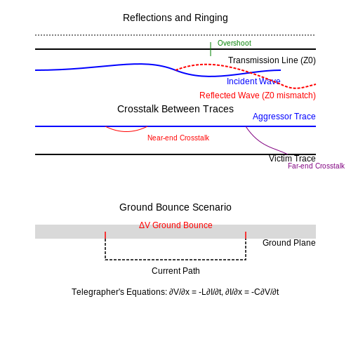
- Reflections: Caused by impedance mismatches, leading to signal ringing and overshoot.
- Crosstalk: Unwanted coupling between adjacent signal traces, inducing noise.
- Attenuation: Frequency-dependent loss due to conductor resistance and dielectric absorption.
- Dispersion: Signal spreading due to frequency-dependent propagation velocities.
- Ground Bounce: Voltage fluctuations in ground/power planes due to transient currents.
Mathematical Foundations
The behavior of signals in transmission lines is described by the telegrapher's equations, derived from Maxwell's equations. For a lossless transmission line:
Where L is inductance per unit length and C is capacitance per unit length. The characteristic impedance Z0 is given by:
Practical Implications
In modern systems with edge rates below 100 ps and data rates exceeding 100 Gbps, signal integrity challenges dominate design constraints. For example:
- PCIe 6.0 requires < 0.5 dB/inch insertion loss at 32 GHz
- DDR5 memory interfaces must maintain timing skews < 1 ps
- 56 Gbps PAM-4 signaling tolerates just 2-3% UI of jitter
Failure to maintain signal integrity manifests as increased bit error rates (BER), reduced noise margins, and in severe cases, complete system failure. Advanced techniques like equalization, pre-emphasis, and sophisticated channel modeling have become essential design tools.
Historical Context
The importance of signal integrity grew exponentially with the transition from kHz-range analog systems to GHz-range digital systems in the 1990s. The seminal work by Howard Johnson and Martin Graham in High-Speed Digital Design (1993) established many foundational SI concepts still in use today.
1.2 Key Parameters Affecting Signal Integrity
Transmission Line Impedance
The characteristic impedance Z0 of a transmission line is a fundamental parameter governing signal integrity. It is determined by the distributed inductance L and capacitance C per unit length:
Mismatched impedances between source, transmission line, and load cause reflections, leading to signal distortion. For high-speed designs, maintaining a controlled impedance (typically 50Ω or 100Ω differential) is critical. Microstrip and stripline configurations are commonly used, with their geometries precisely engineered to achieve the desired Z0.
Propagation Delay and Skew
Propagation delay tpd is the time taken for a signal to traverse the transmission line, given by:
In differential signaling, skew arises when signals on paired lines experience unequal delays due to length mismatches or dielectric variations. Skew exceeding 10% of the bit period can degrade eye diagrams and increase bit error rates. Designers mitigate this through length matching and symmetric routing.
Attenuation and Frequency-Dependent Losses
Signal attenuation is dominated by conductor losses (skin effect) and dielectric losses at high frequencies. The attenuation constant α is frequency-dependent:
Where R is the series resistance and G is the shunt conductance. Above 1 GHz, dielectric absorption (tanδ) becomes significant, necessitating low-loss materials like Rogers 4350B or Isola FR408HR.
Crosstalk
Crosstalk occurs due to capacitive (electric field) and inductive (magnetic field) coupling between adjacent traces. Near-end crosstalk (NEXT) and far-end crosstalk (FEXT) are quantified as:
The 3W rule (spacing traces three times the trace width) reduces crosstalk by 70% compared to minimum spacing. Differential pair routing further suppresses common-mode noise.
Power Integrity Interactions
Power distribution network (PDN) impedance affects signal integrity through simultaneous switching noise (SSN). The target impedance Ztarget for a PDN is derived from:
Where ΔV is the allowable voltage ripple and ΔI is the current transient. Decoupling capacitors must be placed to maintain ZPDN below Ztarget across the entire frequency spectrum.
Jitter Components
Timing jitter decomposes into deterministic (DJ) and random (RJ) components, with total jitter (TJ) at a given bit error rate (BER) calculated as:
The proportionality constant k depends on the BER (e.g., k=14.1 for BER=10-12). Periodic jitter from switching power supplies typically appears as distinct peaks in phase noise plots, while random jitter follows a Gaussian distribution.
Return Path Discontinuities
Incomplete return paths force high-frequency currents to find alternative routes, creating ground bounce and electromagnetic interference (EMI). The partial inductance Lpartial of a disrupted return path is:
Where l is the discontinuity length, d is the distance to the return path, and r is the trace radius. Multi-layer PCBs with dedicated ground planes minimize this effect by providing low-impedance return paths.
1.3 Common Signal Integrity Issues
Reflections and Impedance Mismatch
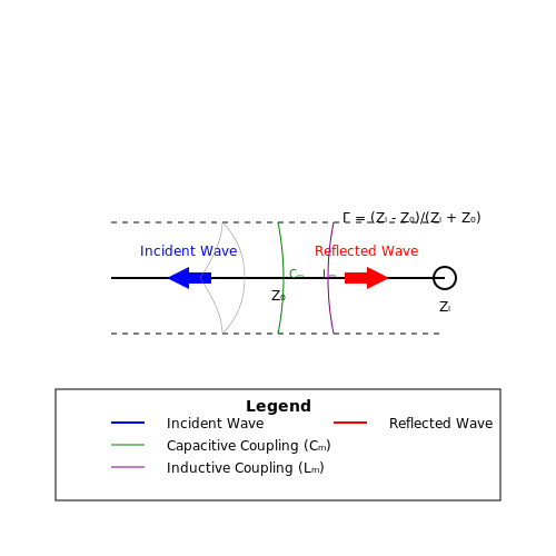
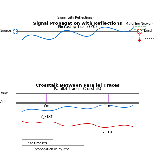
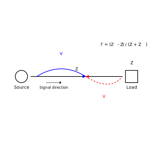
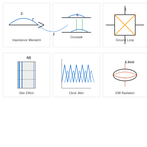
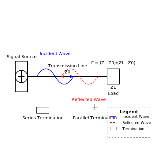
Signal reflections occur when there is an impedance discontinuity along a transmission line, causing partial signal energy to reflect back toward the source. The reflection coefficient (Γ) quantifies this effect:
where ZL is the load impedance and Z0 is the characteristic impedance of the transmission line. When ZL ≠ Z0, reflections distort the signal waveform, leading to overshoot, undershoot, or ringing. In high-speed digital systems (e.g., DDR memory interfaces), even small mismatches (<5%) can cause significant timing errors.
Crosstalk
Crosstalk arises from undesired capacitive (electric field) and inductive (magnetic field) coupling between adjacent traces. Near-end crosstalk (NEXT) and far-end crosstalk (FEXT) are modeled as:
where k is a coupling factor, Cm is mutual capacitance, and Cg is trace-to-ground capacitance. For stripline configurations, inductive coupling dominates at frequencies above 1 GHz. Techniques like guard traces, differential signaling, and increased spacing reduce crosstalk by 15-30 dB.
Power Delivery Network (PDN) Noise
PDN-induced signal integrity issues manifest as simultaneous switching noise (SSN) and ground bounce. The transient current demand (ΔI) creates voltage fluctuations:
where Lloop is the power-ground loop inductance and Rpd is the PDN resistance. In FPGA designs with 100+ simultaneous switches, ground bounce exceeding 50 mV can cause false triggering. Decoupling capacitors must be placed within λ/10 of the noise wavelength to be effective.
Skin Effect and Dielectric Loss
At high frequencies (>1 GHz), current crowds toward the conductor surface (skin effect), increasing effective resistance:
Dielectric loss tangent (tan δ) causes additional attenuation in FR4 substrates (0.02 at 10 GHz). For a 10-inch trace at 5 GHz, these losses can reach 3 dB, necessitating low-Dk materials like Rogers 4350B.
Jitter and Phase Noise
Timing jitter in clock signals has deterministic (DJ) and random (RJ) components. Phase noise (£(f)) relates to jitter through:
In SerDes links operating at 28 Gbps, >1 ps RMS jitter can increase bit error rates beyond 10-12. PLL bandwidth optimization and low-noise power supplies are critical for mitigation.
Electromagnetic Interference (EMI)
Radiated emissions from signal harmonics often violate FCC/CE limits. The electric field strength at 3m distance is:
where A is loop area and I is current. A 100 MHz clock with 10 cm2 loop area can radiate 42 dBμV/m - exceeding Class B limits by 12 dB. Proper shielding and spread-spectrum clocking reduce emissions by 20-40 dB.
2. Characteristics of Transmission Lines
2.1 Characteristics of Transmission Lines
Transmission lines are fundamental in high-frequency signal propagation, where conventional lumped-element circuit models fail. The distributed nature of resistance (R), inductance (L), conductance (G), and capacitance (C) per unit length governs their behavior. At frequencies where the wavelength becomes comparable to the physical length of the line, wave propagation effects dominate.
Telegrapher’s Equations
The voltage and current along a transmission line are described by the telegrapher’s equations, derived from Kirchhoff’s laws applied to an infinitesimal segment of the line:
For sinusoidal steady-state signals, these reduce to phasor forms:
Propagation Constant and Characteristic Impedance
The complex propagation constant γ and characteristic impedance Z₀ are derived from the telegrapher’s equations:
where α is the attenuation constant (Np/m) and β is the phase constant (rad/m). The characteristic impedance is:
For lossless lines (R = G = 0), these simplify to:
Reflection Coefficient and VSWR
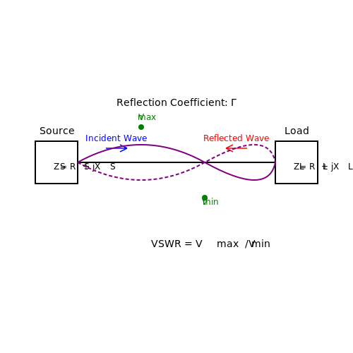
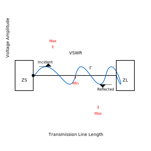
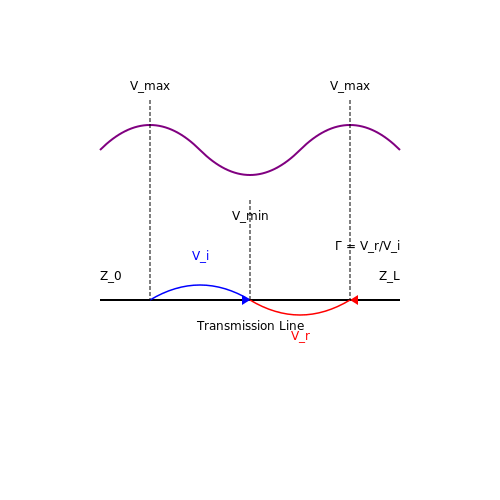
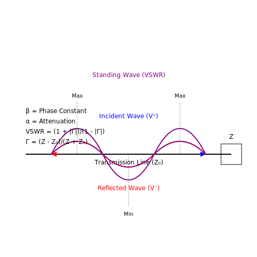
When a transmission line is terminated with an impedance ZL differing from Z₀, reflections occur. The reflection coefficient Γ is:
The voltage standing wave ratio (VSWR) quantifies impedance mismatch:
Practical Implications
- Skin effect: At high frequencies, current crowds near the conductor surface, increasing effective resistance.
- Dispersion: Frequency-dependent propagation velocity causes signal distortion.
- Dielectric losses: Non-ideal insulation materials introduce attenuation.
In PCB design, microstrip and stripline configurations exhibit different effective permittivities due to inhomogeneous dielectric environments, requiring careful modeling of Z₀ and propagation delay.
2.2 Impedance Matching and Reflections
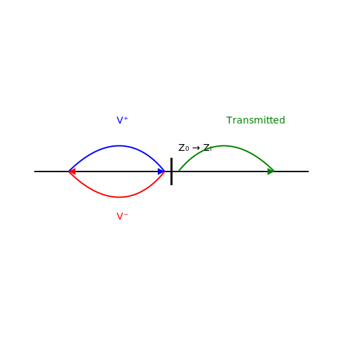
When a signal propagates along a transmission line, impedance mismatches between the source, line, and load cause reflections that degrade signal integrity. The reflection coefficient (Γ) quantifies the magnitude of reflected waves due to impedance discontinuities. For a transmission line with characteristic impedance Z0 terminated by load impedance ZL, the reflection coefficient is:
If ZL = Z0, Γ = 0, and no reflections occur. However, mismatches produce standing waves, increasing insertion loss and distortion. The voltage standing wave ratio (VSWR) further characterizes mismatch severity:
Time-Domain Reflections (TDR)
In high-speed digital systems, reflections manifest as signal overshoot, undershoot, or ringing. A step signal injected into a mismatched transmission line generates reflections observable via time-domain reflectometry (TDR). The round-trip delay (Δt) of the reflection reveals the discontinuity location:
where d is the distance to the mismatch and vp is the propagation velocity.
Impedance Matching Techniques
To minimize reflections, engineers employ:
- Termination resistors – Series or parallel resistors match ZL to Z0.
- Stub matching – Open or shorted transmission line segments cancel reactance.
- Baluns – Convert between balanced and unbalanced lines while matching impedance.
For example, a quarter-wave transformer matches impedances using:
Practical Considerations
In PCB design, controlled impedance routing ensures Z0 consistency. Differential pairs require careful length matching to avoid mode conversion. High-frequency circuits (f > 1 \text{GHz}) demand electromagnetic simulation to account for parasitic effects.
2.3 Propagation Delay and Skew
Fundamentals of Propagation Delay
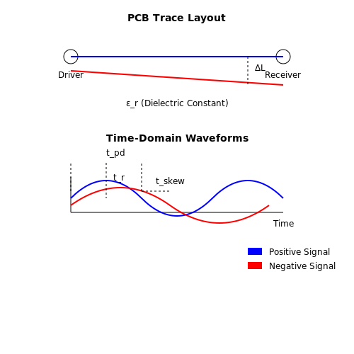
Propagation delay (tpd) is the time taken for a signal to travel from the driver to the receiver in a transmission line. It is determined by the speed of electromagnetic wave propagation in the medium, which is a function of the material's effective dielectric constant (εr). For a lossless transmission line, the propagation delay per unit length is given by:
where c is the speed of light in vacuum (≈ 3×10⁸ m/s). In practical PCB substrates like FR-4 (εr ≈ 4.3), this results in a propagation delay of approximately 5.8 ns/m.
Skew: Causes and Implications
Skew refers to the timing mismatch between signals in parallel transmission paths. It arises from:
- Length mismatches in PCB traces (ΔL)
- Dielectric variations causing localized changes in εr
- Loading differences at receiver ICs
For clock signals in high-speed digital systems (e.g., DDR5 memory interfaces), skew must be controlled to within 5% of the clock period. The skew budget for a 3.2 GHz interface (312 ps period) is typically ≤15 ps.
Differential Pair Skew Analysis
In differential signaling, intra-pair skew (tskew) directly impacts common-mode rejection. The maximum allowable skew is derived from the signal rise time (tr):
For a 28 Gbps SerDes link with tr = 12 ps, this limits skew to 3 ps - requiring length matching to within ±0.5 mm on FR-4.
Measurement Techniques
Modern oscilloscopes measure skew using:
- Time Interval Error (TIE) analysis with picosecond resolution
- Eye diagram bathtub curves for statistical skew distribution
- Vector network analyzers for frequency-domain phase matching
Mitigation Strategies
Advanced routing techniques minimize skew:
- Serpentine traces for length matching with < 0.1% tolerance
- Delay tuning elements like programmable delay lines (Xilinx UltraScale+ offers 1 ps resolution)
- Dielectric constant compensation through via stitching patterns
In 112G PAM-4 systems, adaptive skew compensation algorithms dynamically adjust equalization parameters based on real-time skew measurements.
3. Time-Domain Analysis
3.1 Time-Domain Analysis
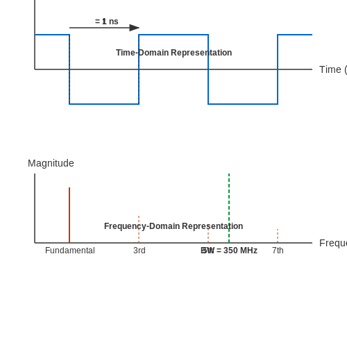
Time-domain analysis examines signal behavior as a function of time, providing direct insight into transient effects, reflections, and distortions in high-speed digital and analog systems. Unlike frequency-domain methods, which rely on Fourier transforms, time-domain analysis captures instantaneous voltage and current variations, making it indispensable for diagnosing signal integrity issues such as overshoot, ringing, and intersymbol interference.
Impulse Response and Step Response
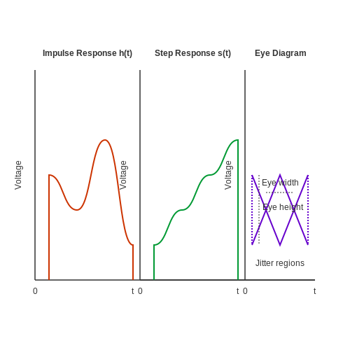
The impulse response h(t) of a linear time-invariant (LTI) system characterizes its output when subjected to an ideal Dirac delta function input. For a transmission line or channel, the step response s(t), derived by integrating h(t), reveals critical metrics like rise time and settling behavior:
For a lossless transmission line with characteristic impedance Z0, the step response exhibits a delay proportional to the propagation velocity vp:
Eye Diagrams
Eye diagrams superimpose multiple unit intervals of a digital signal, visualizing jitter, noise margins, and timing errors. Key parameters extracted from eye diagrams include:
- Eye height: Vertical opening, indicating noise immunity.
- Eye width: Horizontal opening, reflecting timing stability.
- Jitter: Horizontal blurring due to clock deviations.
Time-Domain Reflectometry (TDR)
TDR measures impedance discontinuities by analyzing reflected waveforms from a fast-edge stimulus. The reflection coefficient Γ at a discontinuity is:
where ZL is the load impedance. TDR resolution depends on the rise time tr of the incident pulse, with shorter rise times enabling finer spatial resolution:
Practical Considerations
In high-speed PCB design, time-domain simulations (e.g., SPICE or IBIS models) predict signal integrity issues before fabrication. Non-ideal effects like skin effect and dielectric losses are modeled using empirical equations or tabulated S-parameters converted to the time domain via inverse Fourier transforms.
3.2 Frequency-Domain Analysis
Frequency-domain analysis provides critical insights into signal behavior by decomposing time-domain waveforms into their constituent sinusoidal components. This approach is indispensable for evaluating distortion, noise susceptibility, and transmission line effects in high-speed digital and RF systems.
Fourier Transform Fundamentals
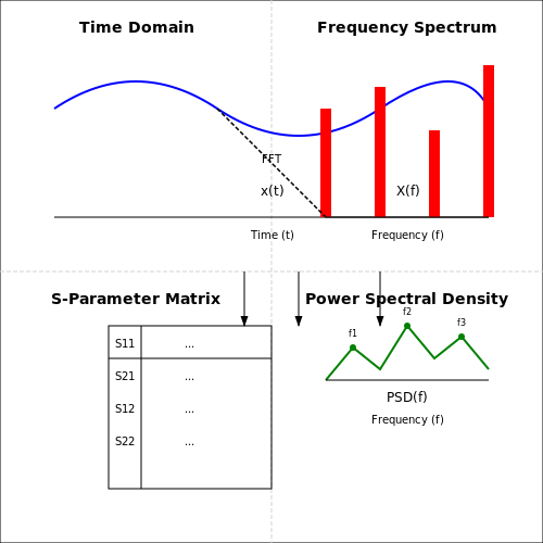
The Fourier transform maps a time-domain signal x(t) into its frequency-domain representation X(f):
For discrete signals, the Discrete Fourier Transform (DFT) is employed:
Key properties impacting signal integrity include:
- Linearity: Superposition applies to spectral components
- Time-shifting: Phase shifts proportional to frequency
- Convolution: Multiplication in frequency domain corresponds to convolution in time domain
S-Parameters in Frequency Domain
Scattering parameters (S-parameters) characterize network behavior at microwave frequencies:
Where S21 represents forward transmission, critical for evaluating channel loss. Practical considerations include:
- Reference impedance matching (typically 50Ω)
- Calibration to remove fixture effects
- Window functions to minimize spectral leakage
Power Spectral Density
Power Spectral Density (PSD) quantifies power distribution across frequencies:
For periodic signals, PSD reveals harmonic content that may cause electromagnetic interference (EMI). In high-speed designs, PSD analysis helps:
- Identify resonant frequencies in power delivery networks
- Quantify crosstalk between adjacent traces
- Optimize clock spreading spectra
Eye Diagram Construction
While traditionally a time-domain tool, eye diagrams derive from frequency-domain concepts through:
- Inverse Fourier transform of channel response
- Convolution with input signal spectrum
- Statistical superposition of bit periods
The resulting eye opening correlates with:
where H(f) is the channel transfer function and X(f) is the input spectrum.
Practical Measurement Techniques
Modern vector network analyzers (VNAs) implement frequency-domain analysis through:
- Stepped-frequency continuous-wave (SFCW) excitation
- Error-corrected heterodyne detection
- Time-domain gating via inverse FFT
Calibration standards (SOLT, TRL) remove systematic errors, while time-domain gating isolates specific discontinuities in transmission lines.
3.3 Eye Diagram Analysis
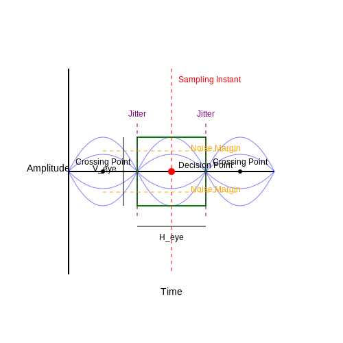
An eye diagram is a powerful graphical tool for assessing signal integrity in high-speed digital communication systems. It is constructed by superimposing multiple unit intervals (UIs) of a digital signal, typically over two to three bit periods, resulting in a pattern resembling an eye. The width and height of the eye opening provide critical insights into timing jitter, noise margins, and intersymbol interference (ISI).
Mathematical Construction of an Eye Diagram
The eye diagram is generated by sampling the received signal y(t) over repeated intervals of duration T, where T is the symbol period. For a signal with N samples per symbol, the eye diagram E(t) can be expressed as:
The vertical eye opening Veye is determined by the difference between the minimum high level and maximum low level at the decision point, while the horizontal eye opening Heye is constrained by timing jitter.
Key Parameters Extracted from Eye Diagrams
- Eye Height: Indicates the noise margin and is measured vertically at the sampling instant.
- Eye Width: Reflects timing stability, measured horizontally at the crossing points.
- Jitter: Quantified by the standard deviation of crossing times.
- Signal-to-Noise Ratio (SNR): Estimated from the vertical eye closure.
Practical Measurement and Interpretation
In real-world systems, eye diagrams are captured using high-bandwidth oscilloscopes with persistence mode enabled. For a signal with bit rate B, the required oscilloscope bandwidth should exceed 0.7B to accurately capture the eye opening. Mask testing, defined by standards such as IEEE 802.3 for Ethernet, is commonly applied to ensure compliance with signal integrity requirements.
Impact of Channel Impairments
Non-ideal channel characteristics, such as frequency-dependent attenuation and group delay variation, distort the eye diagram. The effect of ISI can be modeled using the convolution of the transmitted pulse p(t) with the channel impulse response h(t):
where n(t) represents additive noise. Equalization techniques, such as decision feedback equalizers (DFE) or feed-forward equalizers (FFE), are often employed to mitigate these distortions.
Advanced Analysis: Bathtub Curves and BER Estimation
By slicing the eye diagram at different voltage and timing thresholds, bathtub curves can be generated to predict bit error rates (BER). The BER is related to the Q-factor, which is derived from the eye opening:
where μ1, μ0 are the mean levels of the high and low states, and σ1, σ0 are their respective standard deviations.
4. PCB Layout Best Practices
4.1 PCB Layout Best Practices
Controlled Impedance Routing
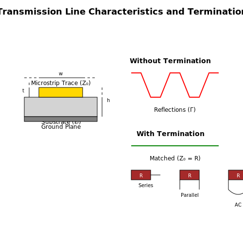
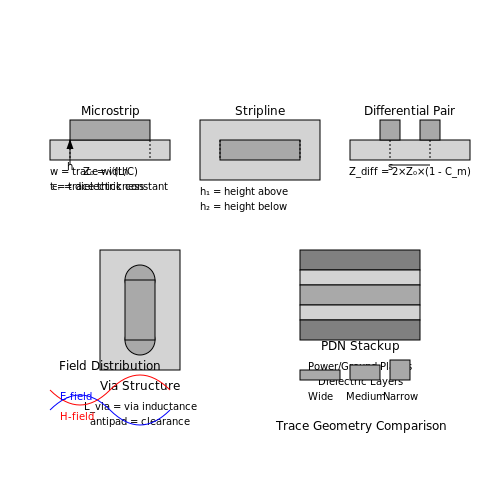
Maintaining controlled impedance is critical for high-speed signal integrity. The characteristic impedance of a transmission line on a PCB is determined by its geometry and dielectric properties. For a microstrip trace, the impedance Z0 is given by:
where ϵr is the dielectric constant, h is the height above the ground plane, w is the trace width, and t is the trace thickness. For striplines, the equation adjusts to account for dual reference planes. Modern PCB design tools incorporate field solvers to compute impedance accurately, but manual verification remains essential for critical designs.
Differential Pair Routing
Differential signaling mitigates noise and crosstalk by exploiting common-mode rejection. Key routing principles include:
- Maintaining consistent spacing to ensure coupling symmetry
- Length matching with serpentine traces where necessary (tolerances < λ/10 at the highest frequency)
- Avoiding reference plane splits beneath pairs to prevent impedance discontinuities
The differential impedance Zdiff relates to single-ended impedance Z0 and coupling coefficient k:
Power Distribution Network (PDN) Design
A low-impedance PDN is achieved through:
- Stackup optimization: Thin dielectrics between power/ground planes reduce plane inductance
- Decoupling capacitor placement: Small-value capacitors must be placed closest to IC power pins
- Via stitching: Multiple vias between planes lower loop inductance
The target impedance Ztarget for the PDN is derived from the maximum allowable voltage ripple ΔV and transient current ΔI:
Crosstalk Mitigation
Far-end crosstalk (FEXT) and near-end crosstalk (NEXT) scale with:
- Trace separation distance (3× dielectric height for -40 dB coupling)
- Parallel run length (critical for timing-sensitive interfaces like DDR)
- Edge rate (faster transitions increase coupling)
The crosstalk voltage Vxtalk between aggressor and victim traces follows:
where Cm is mutual capacitance, Cg is trace-to-ground capacitance, and K is a geometry-dependent factor.
Via Optimization
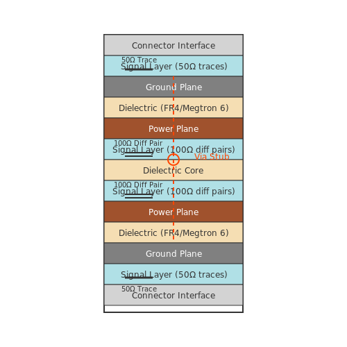
Vias introduce discontinuities characterized by their parasitic inductance Lvia and capacitance Cvia:
Backdrilling (controlled-depth drilling) removes unused via stubs in high-speed designs (>10 Gbps). Differential vias require antipad geometry tuning to maintain impedance matching.
4.2 Termination Techniques
Impedance Matching and Reflections
Signal reflections occur when a transmission line is not properly terminated, leading to impedance mismatches. The reflection coefficient (Γ) quantifies the magnitude of reflected energy and is given by:
where ZL is the load impedance and Z0 is the characteristic impedance of the transmission line. A perfect match (Γ = 0) occurs when ZL = Z0.
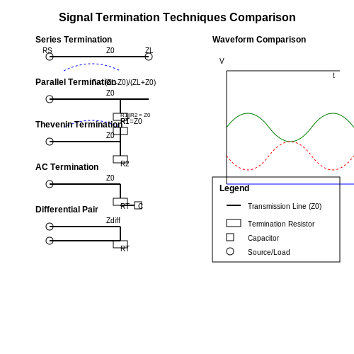
Parallel Termination
Parallel termination places a resistor equal to Z0 at the load end, shunting the signal to ground. This method eliminates reflections but increases power dissipation. The resistor value is critical:
This technique is common in low-frequency applications but becomes inefficient at high speeds due to DC power consumption.
Series Termination
Series termination uses a resistor at the source end to match the driver impedance to the transmission line. The resistor value is calculated as:
where Rout is the output impedance of the driver. This method reduces reflections by absorbing energy at the source but is only effective for point-to-point connections.
Thevenin Termination
Thevenin termination employs a voltage divider network to match impedance while maintaining a defined DC bias. The resistors are selected such that:
This method is useful for bidirectional buses but requires careful power dissipation analysis.
AC Termination
AC termination uses a capacitor in series with the termination resistor to block DC current while maintaining high-frequency matching. The capacitor must be sized to present negligible reactance at the signal frequency:
This technique reduces power consumption but introduces frequency-dependent behavior.
Differential Pair Termination
Differential signaling requires termination between the pair to maintain common-mode rejection. The termination resistor (RT) is equal to the differential impedance (Zdiff):
Proper termination minimizes mode conversion and ensures signal integrity in high-speed differential links.
Active Termination
Active termination uses feedback-controlled circuitry to dynamically adjust termination impedance, compensating for variations in line conditions. This method is prevalent in high-speed memory interfaces (e.g., DDR) where impedance varies with operating conditions.
4.3 Crosstalk Reduction Methods
1. Physical Separation and Routing Techniques
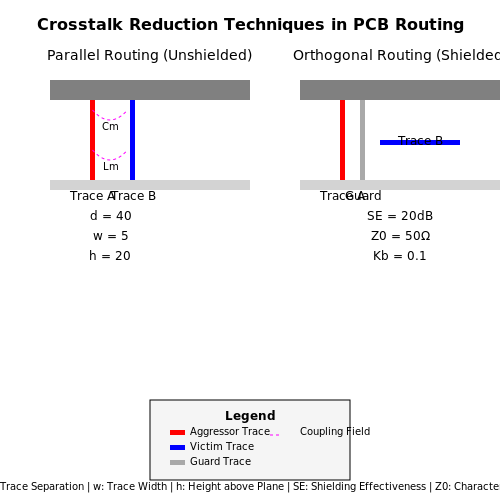
Crosstalk arises due to capacitive and inductive coupling between adjacent signal traces. The mutual capacitance \( C_m \) and mutual inductance \( L_m \) between two parallel traces separated by distance \( d \) scale inversely with \( d \). For a pair of traces with width \( w \) and dielectric thickness \( h \), the crosstalk voltage \( V_{xt} \) can be approximated as:
where \( C_g \) is the trace-to-ground capacitance. Increasing trace separation reduces \( C_m \) and \( L_m \) exponentially. A practical guideline is to maintain \( d \geq 3h \) for microstrip lines and \( d \geq 5w \) for striplines. Differential routing further suppresses crosstalk by ensuring coupled noise appears as a common-mode signal.
2. Ground Shielding and Guard Traces
Inserting a grounded conductor between aggressor and victim traces attenuates electric field coupling. The shielding effectiveness \( SE \) in dB for a guard trace of width \( w_g \) is given by:
For optimal performance, guard traces must be connected to ground at intervals less than \( \lambda/10 \) at the highest frequency of interest. In multilayer boards, dedicated ground planes between signal layers provide superior isolation, reducing crosstalk by 40-60 dB compared to unshielded configurations.
3. Impedance Matching and Termination
Mismatched impedances cause reflections that exacerbate crosstalk. The backward crosstalk coefficient \( K_b \) for a transmission line with characteristic impedance \( Z_0 \) and coupling length \( l \) is:
Proper termination using series or parallel resistors matching \( Z_0 \) minimizes reflections. For differential pairs, maintaining tight impedance control (typically 100Ω ±10%) ensures common-mode rejection ratios above 30 dB.
4. Orthogonal Routing and Layer Stacking
Routing adjacent signal layers perpendicular to each other eliminates parallel coupling regions. This technique reduces crosstalk by 15-20 dB compared to parallel routing. In high-density designs, alternating signal layers with ground/power planes in a symmetric stackup (e.g., Signal-Ground-Signal-Power) creates consistent return paths and contains electromagnetic fields.
5. Slew Rate Control and Edge Rate Limiting
Since crosstalk is proportional to \( \frac{dI}{dt} \), reducing signal edge rates decreases coupled noise. The maximum allowable slew rate \( SR_{max} \) for a target crosstalk level \( V_{xt(max)} \) is:
where \( K_f \) is a geometry-dependent factor. Practical implementations use series resistors (10-33Ω) or adjustable output drivers to achieve rise times of 1-5 ns for critical signals.
6. Frequency Domain Mitigation
For systems with periodic noise sources, spectral spreading techniques such as:
- Spread spectrum clocking (SSC) modulates the clock frequency to disperse interference energy
- Forward error correction (FEC) codes compensate for coupled noise-induced bit errors
- Notch filtering at dominant crosstalk frequencies reduces susceptibility
These methods are particularly effective in reducing deterministic jitter caused by crosstalk in high-speed serial links exceeding 10 Gbps.
7. Advanced Materials and Design Rules
Low-Dk (dielectric constant) materials like Rogers 4350B (Dk=3.48) reduce capacitive coupling, while high-loss laminates (tan δ > 0.01) attenuate resonant coupling. Modern design rules enforce:
- 3W rule (center-to-center spacing ≥ 3× trace width)
- Differential pair skew matching < ±5 ps/inch
- Via stitching at < λ/4 intervals for ground continuity
These techniques collectively enable crosstalk suppression of 50-70 dB in state-of-the-art PCB designs operating at 56+ Gbps PAM4 signaling.
5. High-Speed Digital Design Considerations
5.1 High-Speed Digital Design Considerations
Transmission Line Effects
At high frequencies, interconnects behave as transmission lines rather than ideal conductors. The signal propagation delay becomes comparable to the signal rise time, leading to reflections, ringing, and impedance mismatches. The characteristic impedance Z0 of a transmission line is given by:
where L is the distributed inductance per unit length and C is the distributed capacitance per unit length. For microstrip traces on a PCB, Z0 typically ranges from 50Ω to 75Ω, while striplines are often designed for 50Ω.
Signal Reflections and Termination
When a signal encounters an impedance discontinuity, a portion reflects back toward the source. The reflection coefficient Γ is:
where ZL is the load impedance. To minimize reflections, termination strategies such as series, parallel, or AC termination are employed. Series termination (source termination) is common in point-to-point topologies, while parallel termination is used in multi-drop buses.
Crosstalk and Coupling
Electromagnetic coupling between adjacent traces introduces crosstalk, categorized as:
- Forward Crosstalk (Near-End): Occurs in the same direction as signal propagation.
- Backward Crosstalk (Far-End): Appears at the opposite end of the aggressor line.
The crosstalk voltage Vxtalk depends on mutual capacitance Cm and mutual inductance Lm:
where k is a coupling factor. Spacing traces at least 3× the dielectric height apart reduces crosstalk.
Power Integrity and Simultaneous Switching Noise
High-speed designs demand low-impedance power delivery networks (PDNs) to mitigate voltage droops caused by simultaneous switching outputs (SSO). The target impedance Ztarget is:
where ΔV is the allowable voltage ripple and ΔI is the current transient. Decoupling capacitors must be placed close to IC power pins to minimize loop inductance.
Differential Signaling
Differential pairs reject common-mode noise and reduce electromagnetic interference (EMI). The differential impedance Zdiff for a tightly coupled pair is:
where k is the coupling coefficient. Maintaining symmetry in trace length and spacing is critical to preserve signal integrity.
Skin Effect and Dielectric Losses
At high frequencies, current crowds near the conductor surface (skin effect), increasing resistance. The skin depth δ is:
where ρ is resistivity, μ is permeability, and f is frequency. Dielectric losses, quantified by the loss tangent (tan δ), further attenuate signals, necessitating low-loss materials like Rogers or Isola laminates for multi-gigabit designs.
5.2 Signal Integrity in RF and Microwave Circuits
Signal integrity in RF and microwave circuits is governed by high-frequency effects that become significant as wavelengths approach the physical dimensions of transmission structures. At these frequencies, parasitic elements, impedance mismatches, and electromagnetic interference (EMI) dominate performance degradation.
Transmission Line Theory at RF Frequencies
The distributed-element model replaces lumped-element approximations when signal wavelengths (
where
Skin Effect and Dielectric Loss
At microwave frequencies, current density concentrates near conductor surfaces (skin effect), increasing effective resistance. The skin depth (
where
Impedance Matching Techniques
Mismatches cause standing waves, quantified by the voltage standing wave ratio (VSWR). Quarter-wave transformers and stub matching networks are common solutions. For a load impedance
Crosstalk and Radiation
Electromagnetic coupling between adjacent traces introduces near-end (NEXT) and far-end (FEXT) crosstalk. The coupling coefficient for microstrips depends on spacing (
Radiation losses become non-negligible above 10 GHz, requiring shielded enclosures or substrate-integrated waveguides (SIWs).
Practical Mitigation Strategies
- Controlled impedance routing: Use EM solvers to validate trace geometries for target
- Material selection: Low-loss dielectrics like Rogers RO4003C for reduced
5.3 Power Integrity and Its Impact on Signal Integrity
Power Distribution Network (PDN) Fundamentals
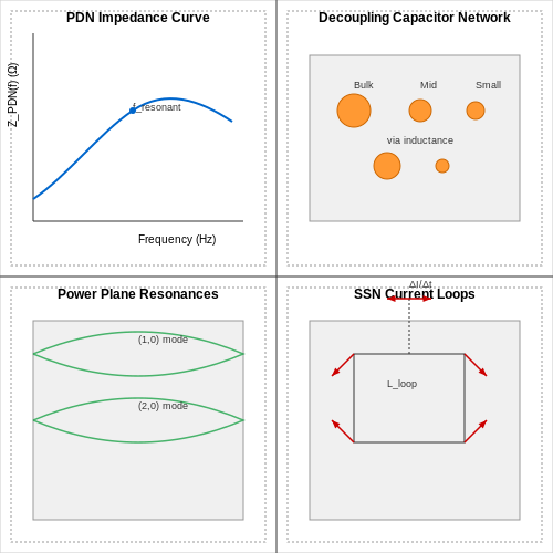
The power distribution network in high-speed circuits must maintain a stable voltage across all operating conditions. Any deviation from the target voltage manifests as power supply noise, which directly couples into signal paths through parasitic capacitance and shared return paths. The PDN impedance ZPDN(f) determines how effectively the network suppresses noise at different frequencies:
where R, L, and C represent the equivalent resistance, inductance, and capacitance of the PDN. At frequencies above the PDN's self-resonant frequency, the impedance becomes dominated by inductance, leading to voltage droops during rapid current transients.
Simultaneous Switching Noise (SSN)
When multiple digital drivers switch simultaneously, the sudden current demand (di/dt) causes inductive voltage drops across the PDN. This ground bounce or VCC sag appears as common-mode noise on signal lines, reducing noise margins. The peak noise voltage can be derived from:
Here, Lloop is the loop inductance of the PDN, N is the number of switching drivers, and ΔI/Δt is the current slew rate. In DDR5 memory systems, for example, SSN can exceed 200mV if not properly managed through decoupling strategies.
Decoupling Capacitor Network Design
Effective decoupling requires a multi-tiered capacitor network spanning frequency decades:
- Bulk capacitors (10-100μF) handle low-frequency current demands
- Ceramic capacitors (0.1-10μF) target mid-range frequencies
- High-frequency MLCCs (1-100nF) suppress GHz-range noise
The optimal placement follows the 10× rule: each capacitor should be an order of magnitude smaller than the previous tier, with the smallest placed closest to the load. The effective impedance bandwidth is given by:
where Lvia includes the parasitic inductance of interconnects between the capacitor and power plane.
Power Plane Resonance Effects
Power and ground planes form distributed cavity resonators that exhibit standing wave patterns at frequencies determined by their physical dimensions. For rectangular planes of length a and width b, the resonant frequencies are:
where c is the speed of light, εr is the dielectric constant, and m,n are mode integers. These resonances can amplify noise at specific frequencies, requiring strategic placement of damping components or plane segmentation.
Impact on Signal Quality Metrics
Power integrity issues manifest in signal integrity measurements through:
- Increased jitter from supply-modulated propagation delays
- Reduced eye opening due to noise coupling into differential pairs
- Elevated BER from timing uncertainty and amplitude noise
In SerDes systems operating at 56Gbps and beyond, power supply induced jitter (PSIJ) often contributes over 30% of the total jitter budget. Measurement techniques like power-aware eye diagrams correlate voltage ripple with signal degradation.
Mitigation Techniques
Advanced PCB design strategies address power-signal coupling:
- Differential power delivery using dedicated power/ground via pairs
- Embedded capacitance with thin dielectrics between power planes
- Active voltage regulation using point-of-load converters with >100MHz bandwidth
- Frequency-domain spreading through spread-spectrum clocking
In 3D-IC implementations, through-silicon vias (TSVs) reduce loop inductance by an order of magnitude compared to wirebond interconnects, significantly improving high-frequency power delivery.
6. Recommended Books and Papers
6.1 Recommended Books and Papers
- PDF Signal and Power Integrity — Simplified - pearsoncmg.com — Chapter 1 Signal Integrity Is in Your Future 1 1.1 What Is Signal Integrity? 2 1.2 Signal Quality on a Single Net 5 1.3 Cross Talk 9 1.4 Rail-Collapse Noise 11 1.5 Electromagnetic Interference (EMI) 13 1.6 Two Important Signal Integrity Generalizations 16 1.7 Trends in Electronic Products 16 1.8 The Need for a New Design Methodology 22
- SIGNAL INTEGRITY AND RADIATED EMISSION - Wiley Online Library — 1 Introduction to Signal Integrity and Radiated Emission in a Digital System 1 1.1 Power and Signal Integrity 2 1.1.1 Power Distribution Network 3 1.1.2 Signal Distribution Network 5 1.1.3 Noise Limitations and Design for Characteristic Impedance 7 1.2 Radiated Emission 9 1.2.1 Definition of Radiated Emission Sources 9 1.2.2 Radiated Emission ...
- PDF Advanced Signal Integrity for High-Speed Digital Designs - SKAT-PRO — 1. Introduction: The Importance of Signal Integrity 1 1.1 Computing Power: Past and Future, 1 1.2 The Problem, 4 1.3 The Basics, 5 1.4 A New Realm of Bus Design, 7 1.5 Scope of the Book, 7 1.6 Summary, 8 References, 8 2. Electromagnetic Fundamentals for Signal Integrity 9 2.1 Maxwell's Equations, 10 2.2 Common Vector Operators, 13 2.2.1 ...
- PDF Advanced Signal Integrity for High-speed Digital Designs — 1. Introduction: The Importance of Signal Integrity 1. 1.1 Computing Power: Past and Future, 1 1.2 The Problem, 4 1.3 The Basics, 5 1.4 A New Realm of Bus Design, 7 1.5 Scope of the Book, 7 1.6 Summary, 8 References, 8. 2. Electromagnetic Fundamentals for Signal Integrity 9. 2.1 Maxwell™s Equations, 10 2.2 Common Vector Operators, 13 2.2.1 ...
- PDF The Foundations of Signal Integrity - SKAT-PRO — The foundations of signal integrity / Paul G. Huray. p. cm. Includes bibliographical references and index. ISBN 978--470-34360-9 1. Signal integrity (Electronics) 2. Electromagnetic interference—Prevention. 3. Electric lines. I. Title. TK7867.2.H87 2010 621.382′2-dc22 2009018610 Printed in the United States of America 10 9 8 7 6 5 4 3 2 1
- Signal and Power Integrity - Simplified | Pearson eLibrary — This book brings together up-to-the-minute techniques for finding, fixing, and avoiding signal integrity problems in your design. Drawing on his work teaching several thousand engineers and graduate students, world-renowned expert Eric Bogatin systematically presents the root causes of all six families of signal integrity, power integrity, and ...
- PDF S I Signal Integrity - download.e-bookshelf.de — Signal Integrity From High-speed to Radiofrequency Applications FOCUS Fabien Ndagijimana D IGT AL SNM EP ROC FOCUS SERIES in DIGITAL SIGNAL AND IMAGE PROCESSING www.iste.co.uk Z(7ib8e8-CBFFAE(W550-Ndagijimana.qxp_Layout 1 24/04/2014 16:03 Page 1
- Signal Integrity - Simplified[Book] - O'Reilly Media — Book description. The complete guide to understanding and designing for signal integrity. Suitable for even non-specialists, Signal Integrity—Simplified offers a comprehensive, easy-to-follow look at how physical interconnects affect electrical performance. World-class engineer Eric Bogatin expertly reviews the root causes of the four families of signal integrity problems and offers ...
- PDF HIGH-SPEED DIGITAL SYSTEM DESIGN - Wiley — This book is printed on acid-free paper. ... Electronic digital computers—Design and construction. 2. Very high speed integrated circuits—Design and construction. 3. Microcomputers—Buses. ... 9.2.5 Signal Integrity 209 9.3 Design Optimization 210 9.3.1 Paper Analysis 211 9.3.2 Routing Study 212
- Signal Integrity: Applied Electromagnetics and Professional Practice ... — Emphasis is placed on real problems that the author has encountered in his professional career, integrating problem-solving strategies and real signal-integrity case studies throughout the presentation. Students are challenged to think about managing complex design projects and implementing successful engineering and manufacturing processes.
6.2 Online Resources and Tutorials
- PDF Signal and Power Integrity — Simplified - pearsoncmg.com — Chapter 1 Signal Integrity Is in Your Future 1 1.1 What Is Signal Integrity? 2 1.2 Signal Quality on a Single Net 5 1.3 Cross Talk 9 1.4 Rail-Collapse Noise 11 1.5 Electromagnetic Interference (EMI) 13 1.6 Two Important Signal Integrity Generalizations 16 1.7 Trends in Electronic Products 16 1.8 The Need for a New Design Methodology 22
- PDF S-Parameters for Signal Integrity - Cambridge University Press & Assessment — only for signal integrity professionals, but for any microwave engineer. Andrea Ferrero, Keysight This book provides unique and consistent description of s-parameters use for analysis of linear networks, and signal measurement and processing in one volume, supplemented and illustrated with free open-source signal integrity software.
- Home Page | Signal Integrity Journal — Signal Integrity Journal, a sister publication to Microwave Journal, covers signal integrity, power integrity and EMC/EMI related topics with industry news, technical articles, white papers, products, Buyer's Guide, webinars, videos and more. The vision for the SI Journal is to increase the signal to noise ratio for SI, PI and EMC engineers by providing high value content.
- Signal Integrity - Simplified[Book] - O'Reilly Media — Book description. The complete guide to understanding and designing for signal integrity. Suitable for even non-specialists, Signal Integrity—Simplified offers a comprehensive, easy-to-follow look at how physical interconnects affect electrical performance. World-class engineer Eric Bogatin expertly reviews the root causes of the four families of signal integrity problems and offers ...
- Transmission Lines in Digital and Analog Electronic Systems — not be available in electronic formats. For more information about Wiley products, visit our web site at www.wiley.com. Library of Congress Cataloging-in-Publication Data: Paul, Clayton R. Transmission lines in digital and analog electronic systems : signal integrity and crosstalk / Clayton R. Paul. p. cm. ISBN 978--470-59230-4 1.
- Signal and Power Integrity - Simplified | Pearson eLibrary — For professionals and students at all levels of experience, this book emphasizes intuitive understanding, practical tools, and engineering discipline, rather than theoretical derivation or mathematical rigor. It has earned a well-deserved reputation as the #1 resource for getting signal integrity designs right—first time, every time.
- ANSYS Electronics Desktop: Simple Communications Channel For Signal ... — This tutorial describes how to specify and run QuickEye and VerifEye analyses in order to perform signal integrity analyses. ANSYS Electronics Desktop integrates rigorous electromagnetic analysis with system and circuit simulation in a comprehensive, easy-to-use design platform.
- Transmission lines in digital and analog electronic systems : signal ... — A much-needed primer on all aspects of transmission lines for electric and computer engineering graduatesMost of today's electrical engineering and computer engineering graduates lack a critically important skill: the analysis of transmission lines. They need this basic knowledge in order to be able to design high-speed digital and high-frequency analog systems-and this problem will only get ...
- 6.02 Tutorial 1 | Introduction to EECS II: Digital Communication ... — This resource contains information regarding tutorial 1. 6.02 Tutorial 1 | Introduction to EECS II: Digital Communication Systems | Electrical Engineering and Computer Science | MIT OpenCourseWare Browse Course Material
- Introduction to EECS II: Digital Communication Systems | Electrical ... — An introduction to several fundamental ideas in electrical engineering and computer science, using digital communication systems as the vehicle. The three parts of the course—bits, signals, and packets—cover three corresponding layers of abstraction that form the basis of communication systems like the Internet. The course teaches ideas that are useful in other parts of EECS: abstraction ...
6.3 Industry Standards and Guidelines
- PDF Federal Information Processing Standards Publication: electronic data ... — The Federal Information Processing Standards Publications Series of the National Institute of Standards and Technology (NIST) is the official publication relating to standards and guidelines adopted and promulgated under the provisions of Section 5131 of the Information Technology Management Reform Act of 1996, and the Computer Security Act of ...
- PDF A Guide to United States Electrical and Electronic Equipment ... - NIST — Electrical and Electronic Equipment Compliance Requirements HOW TO USE THIS GUIDE Regulations are mandatory Standards are voluntary (unless "Incorporated by Reference", or prescribed as performance standards, in a regulation) Guidelines may be voluntary (but are often de facto industry standards) "Red" text highlights mandatory requirements
- IEC 61000-6-3 - Electromagnetic compatibility (EMC) - Part 6-3: Generic ... — IEC 61000-6-3:2020 is a generic EMC emission standard applicable only if no relevant dedicated product or product family EMC emission standard has been published. This part of IEC 61000 for emission requirements applies to electrical and electronic equipment intended for use at residential (see 3.1.14) locations.
- PDF IEC 61204-3:2016 - IEC 61204-3:2016 RLV - cdn.standards.iteh.ai — The International Electrotechnical Commission (IEC) is the leading global organization that prepares and publishes International Standards for all electrical, electronic and related technologies.
- 6.4.1. High-Speed Serial Interface Signal Integrity Design Guidelines — The Agilex™ 7 High-Speed Serial Interface (HSSI) Signal Integrity (SI) Design Guidelines provide information on supported protocols, channel loss budget calculations, PCB materials and stackup, and tile-specific design guidelines.
- US EMC Published Standards | National Standards Institute — Scope: This standard is intended to include procedures for compliance testing of several different types of Wireless Power Transfer (WPT) products with applicable electromagnetic compatibility (EMC) and radio regulatory requirements. Test procedures will focus on radiated field and conducted measurements and may reference established standards.
- PDF Signal and Power Integrity Simplified - pearsoncmg.com — Since the publication of the first edition of Signal Integrity—Simplified, the princi-ples of signal integrity haven't changed. What has changed, though, is the prolific use of high-speed serial links and the critical role power integrity now plays in the success or failure of new product introductions.
- Appendix B: List of Design Standards | GlobalSpec — IPC-7351, Generic Requirements for Surface-Mount Design and Land Pattern Standard IPC-9252, Guidelines and Requirements for Electrical Testing of Unpopulated Printed Boards
- PDF Signal Integrity DesignGuide - Keysight — Note 1 The JEDEC (Joint Electronic Device Engineering Council) Solid State Technology Association is a semiconductor engineering standardization body of the Electronic Industries Alliance (EIA), a trade association that represents all areas of the electronic industry.
- PDF IPC-A-610G: Acceptability of Electronic Assemblies table of contents — This document presents acceptance requirements for the manufacture of electrical and electronic assemblies. Historically, elec-tronic assembly standards contained a more comprehensive tutorial addressing principles and techniques.