High-Frequency Impedance Matching
1. Definition and Importance of Impedance Matching
1.1 Definition and Importance of Impedance Matching
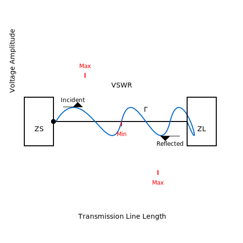
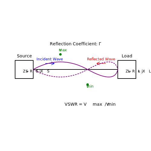
Impedance matching is the process of designing a network that ensures maximum power transfer between a source and a load by making their impedances complex conjugates of each other. At high frequencies, this becomes critical due to transmission line effects, where mismatches lead to standing waves, signal reflections, and degraded system performance.
Fundamental Theory
The power transfer between a source with impedance ZS = RS + jXS and a load ZL = RL + jXL is maximized when:
where ZS* denotes the complex conjugate of the source impedance. This condition ensures that the reactive components cancel out, and the real parts are equal, minimizing reflected power.
Reflection Coefficient and VSWR
The degree of impedance mismatch is quantified by the reflection coefficient Γ:
When Γ = 0, perfect matching is achieved. The Voltage Standing Wave Ratio (VSWR) provides another measure:
In practical RF systems, a VSWR below 1.5:1 is often targeted, corresponding to |Γ| ≤ 0.2.
High-Frequency Considerations
At microwave frequencies (above 1 GHz), several factors complicate impedance matching:
- Transmission line effects: Distributed elements must be treated as waveguides rather than lumped components.
- Parasitic reactances: Stray capacitance and inductance become significant compared to operating wavelengths.
- Skin effect: Current crowding increases conductor loss at high frequencies.
- Dielectric losses: Substrate materials exhibit frequency-dependent loss tangents.
These effects make broadband matching particularly challenging, often requiring multi-section matching networks or active tuning circuits.
Practical Applications
Proper impedance matching is essential in:
- RF power amplifiers (to maximize output power and efficiency)
- Antenna systems (to minimize reflected power and optimize radiation patterns)
- High-speed digital circuits (to prevent signal integrity issues from reflections)
- Microwave test equipment (for accurate measurements)
Modern techniques include adaptive impedance tuning using varactor diodes or MEMS switches, particularly in reconfigurable systems operating across multiple frequency bands.
1.2 Key Parameters in High-Frequency Circuits
High-frequency circuits operate under constraints that differ significantly from their low-frequency counterparts. Understanding the governing parameters is essential for designing efficient impedance-matching networks.
Characteristic Impedance (Z0)
The characteristic impedance of a transmission line, denoted as Z0, is a fundamental parameter defined as the ratio of voltage to current in a propagating wave. For a lossless transmission line, it is given by:
where L is the distributed inductance per unit length and C is the distributed capacitance per unit length. At high frequencies, deviations from Z0 lead to reflections, degrading signal integrity.
Reflection Coefficient (Γ)
When a transmission line is terminated with an impedance ZL differing from Z0, a portion of the incident wave reflects back. The reflection coefficient Γ quantifies this mismatch:
For perfect matching, Γ = 0, implying no reflections. In practice, |Γ| < 0.1 (VSWR < 1.22) is often targeted to minimize power loss.
Quality Factor (Q)
The quality factor Q measures the bandwidth selectivity of resonant circuits. For a series RLC network:
where ω0 is the resonant frequency. High-Q circuits exhibit narrow bandwidths, making them sensitive to component tolerances in impedance-matching applications.
Scattering Parameters (S-Parameters)
At microwave frequencies, S-parameters replace traditional impedance matrices. The S-matrix describes how power propagates through a multi-port network:
where an and bn represent incident and reflected waves, respectively. S11 and S22 directly relate to input and output impedance matching.
Skin Effect and Dielectric Loss
At high frequencies, current density becomes non-uniform across conductors due to the skin effect, increasing effective resistance:
where δ is the skin depth, μ is permeability, and σ is conductivity. Dielectric losses, quantified by the loss tangent (tan δ), further attenuate signals in substrates like FR4 at GHz frequencies.
Practical Implications
- Microstrip Design: Z0 depends on trace width, substrate height, and dielectric constant (εr). A 50Ω standard minimizes reflections in RF systems.
- Component Selection: Parasitic inductance and capacitance dominate at high frequencies, necessitating surface-mount devices (SMDs) with minimal lead lengths.
- Simulation Tools: Electromagnetic simulators (e.g., ADS, HFSS) model S-parameters and dispersion effects that analytical equations approximate poorly.
Reflection Coefficient and VSWR
Definition of the Reflection Coefficient
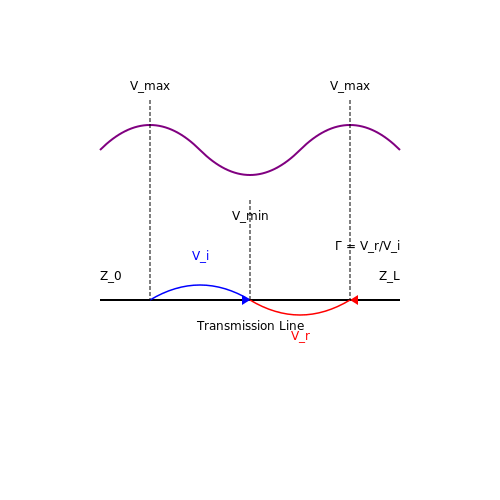
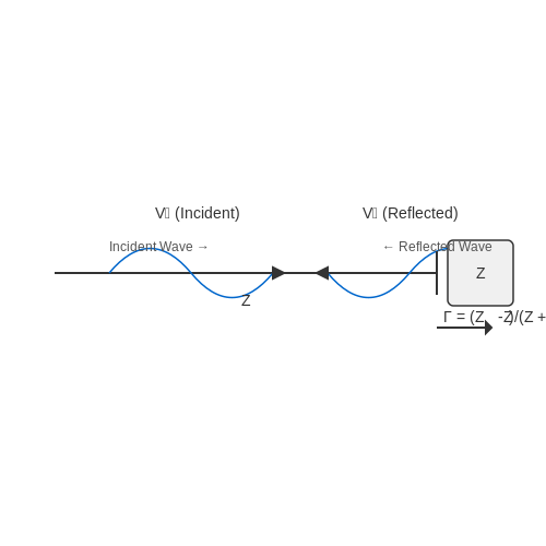
The reflection coefficient (Γ) quantifies the fraction of an incident electromagnetic wave reflected due to impedance mismatch at a boundary between two transmission media. For a transmission line with characteristic impedance Z0 terminated by a load impedance ZL, the voltage reflection coefficient is given by:
This complex quantity encodes both magnitude and phase shift of the reflected wave. A perfect match (ZL = Z0) yields Γ = 0, while total reflection occurs at open (Γ = +1) or short (Γ = -1) terminations.
Relationship to Power and Standing Waves
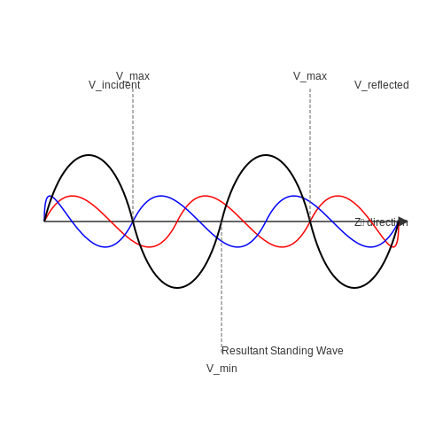
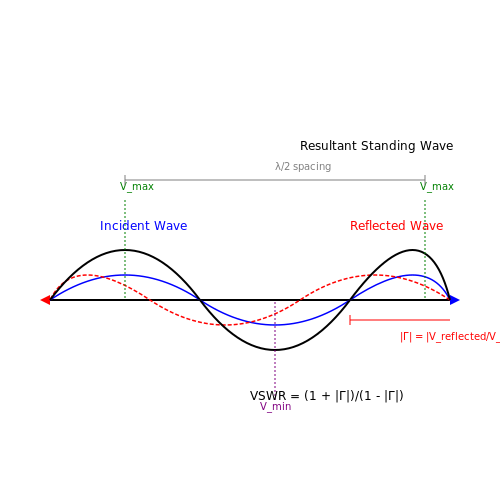
The power reflection coefficient |Γ|2 determines the proportion of incident power reflected. The forward and reflected waves interfere, creating a standing wave pattern characterized by the voltage standing wave ratio (VSWR):
VSWR ranges from 1 (perfect match) to ∞ (total reflection). Practical systems often specify VSWR thresholds (e.g., <2:1 for antenna systems) to limit reflected power.
Measurement and Practical Implications
VSWR is measurable using a slotted line or vector network analyzer. High VSWR indicates:
- Reduced power transfer due to reflected energy
- Increased losses in feedlines and amplifiers
- Potential damage to transmitter components from reflected power
In radar systems, mismatches distort pulse shapes and reduce sensitivity. Satellite communications often employ automatic impedance tuning to maintain VSWR <1.5:1 across operational bands.
Smith Chart Visualization
The Smith chart provides a graphical representation of reflection coefficient behavior:
Constant VSWR circles appear as concentric rings centered at Γ=0, with impedance/admittance coordinates overlaid for matching network design.
Frequency-Dependent Effects
At high frequencies, the reflection coefficient becomes frequency-dependent due to:
- Transmission line dispersion
- Load impedance variations (e.g., antenna resonance shifts)
- Parasitic reactances in connectors and components
Broadband matching requires minimizing |Γ(f)| across the operational bandwidth, often necessitating multi-section matching networks or active tuning.
2. L-Section Matching Networks
2.1 L-Section Matching Networks
L-section matching networks are the simplest and most widely used impedance matching circuits, consisting of two reactive elements (inductor and capacitor) arranged in an "L" configuration. These networks transform a given load impedance (ZL) to a desired source impedance (ZS) at a specific frequency, minimizing reflections and maximizing power transfer.
Fundamental Operation
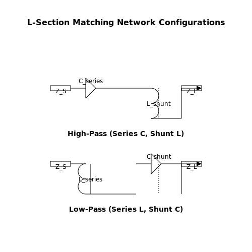
An L-network operates by introducing conjugate impedance matching. For a load impedance ZL = RL + jXL, the matching network must present an impedance Zin = RS − jXS to the source, where RS is the source resistance and XS cancels the load reactance. The two possible configurations are:
- High-pass configuration (series capacitor, shunt inductor)
- Low-pass configuration (series inductor, shunt capacitor)
Design Equations
For a load impedance ZL = RL + jXL and source impedance ZS = RS + j0, the required reactances (X1 and X2) for the low-pass L-network are derived as follows:
where Rhigh = max(RS, RL) and Rlow = min(RS, RL). The sign of X1 and X2 determines whether the elements are inductive (positive) or capacitive (negative).
Practical Considerations
L-networks are narrowband due to their frequency-dependent reactances. The quality factor (Q) is fixed by the impedance transformation ratio, limiting their use in applications requiring high selectivity. For wider bandwidth, multi-section networks (e.g., π or T-networks) are preferred.
Component Losses
Real-world inductors and capacitors exhibit parasitic resistance, which degrades matching efficiency. The unloaded Q of reactive components must be sufficiently high to minimize insertion loss:
Applications
L-sections are commonly used in RF amplifiers, antenna matching, and filter interfaces. Their simplicity makes them ideal for fixed-frequency systems where tuning flexibility is unnecessary.
2.2 Pi and T-Section Matching Networks
Fundamentals of Pi and T-Section Networks
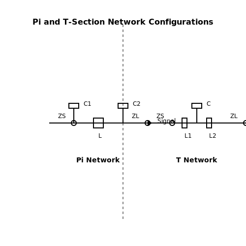
Pi (π) and T-section networks are reactive ladder structures used in high-frequency impedance matching. These topologies consist of three reactive elements arranged in either a Pi (shunt-series-shunt) or T (series-shunt-series) configuration. The choice between them depends on the source/load impedance, frequency range, and practical constraints like component parasitics.
Pi-Network Analysis
A Pi-network comprises two shunt capacitors (C1, C2) and a series inductor (L). The matching condition is derived from the ABCD parameters of the network. For a load impedance ZL and source impedance ZS, the matching equations are:
where A, B, C, and D are the transmission matrix parameters of the Pi-network. Solving for the components yields:
Here, RS and RL are the real parts of ZS and ZL, respectively, and ω is the angular frequency.
T-Network Analysis
The T-network uses two series inductors (L1, L2) and a shunt capacitor (C). Its matching conditions are similarly derived from ABCD parameters. For a given ZS and ZL, the component values are:
T-networks are particularly useful when the load impedance is higher than the source impedance, as they provide better control over the quality factor (Q).
Quality Factor and Bandwidth Considerations
The loaded Q of a matching network determines its bandwidth. For Pi and T-networks, the Q is given by:
where Rhigh is the larger of RS or RL, and Rlow is the smaller resistance. Higher Q results in narrower bandwidth, which is often undesirable in broadband applications.
Practical Design Considerations
In real-world implementations, component parasitics (e.g., ESR in capacitors, stray capacitance in inductors) must be accounted for. Additionally, the self-resonant frequency (SRF) of reactive elements limits the usable frequency range. Computer-aided tools like Smith charts or RF simulation software (e.g., ADS, SPICE) are often employed for optimization.
Applications in RF Systems
Pi and T-networks are widely used in:
- RF power amplifiers to match transistor output impedance to the load.
- Antenna tuners to compensate for impedance mismatches.
- Filter design as part of impedance transformation stages.
For instance, in a 50Ω to 75Ω matching scenario at 100 MHz, a Pi-network might use C1 = 10.6 pF, L = 79.6 nH, and C2 = 7.1 pF, while a T-network would require L1 = 39.8 nH, C = 21.2 pF, and L2 = 59.7 nH.
2.3 Stub Matching Techniques
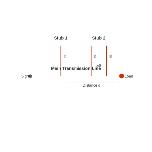
Stub matching is a widely used method for impedance matching in high-frequency circuits, particularly in transmission line systems. The technique involves introducing a short or open-circuited transmission line segment (a stub) in parallel or series with the main line to cancel out reactive components and achieve a matched impedance condition.
Single-Stub Matching
Single-stub matching employs one stub placed at a specific distance from the load to achieve impedance matching. The process involves two key steps:
- Determining the stub position: The distance from the load where the normalized admittance has a real part equal to 1 (conductance matching).
- Calculating the stub length: The length of the stub required to cancel the susceptance at the chosen position.
The normalized admittance at distance d from the load is given by:
where Γ(d) is the reflection coefficient at distance d from the load. The stub length l is calculated to provide a susceptance that cancels the imaginary part of Y(d):
Double-Stub Matching
Double-stub matching provides more flexibility by using two stubs at fixed separation distances (typically λ/8 or λ/4). This method is particularly useful when single-stub matching is impractical due to physical constraints.
The design procedure involves:
- Plotting the normalized admittance on a Smith chart
- Rotating the admittance point by the fixed stub separation distance
- Determining the required stub lengths to transform the admittance to the center of the chart
The mathematical formulation becomes more complex, involving the solution of simultaneous equations for the stub susceptances:
Practical Considerations
In real-world applications, several factors must be considered:
- Frequency sensitivity: Stub matching is inherently narrowband, with performance degrading as frequency moves away from the design point.
- Implementation losses: Practical stubs introduce some loss due to finite conductor conductivity and dielectric losses.
- Physical constraints: The achievable stub lengths may be limited by board space or mechanical considerations.
Modern implementations often use microstrip or stripline stubs in PCB designs, with careful attention to dispersion effects and edge coupling. For broadband applications, multiple stubs or tapered matching sections may be employed.
2.4 Transformer-Based Matching
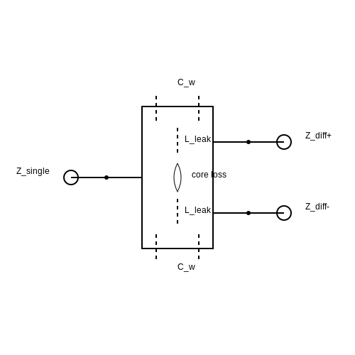
Transformer-based impedance matching leverages mutual inductance to achieve efficient power transfer between circuits with mismatched impedances. At high frequencies, the parasitic capacitance and leakage inductance of practical transformers introduce non-ideal behavior, necessitating careful design to minimize losses and maintain broadband performance.
Ideal Transformer Model
An ideal transformer with turns ratio N transforms impedances according to:
where Zin is the input impedance and ZL is the load impedance. The power transfer is lossless, with perfect coupling (k = 1) and infinite primary inductance.
Non-Ideal Effects at High Frequencies
Practical transformers exhibit:
- Leakage inductance (Lleak): Limits high-frequency response by introducing a parasitic reactance.
- Winding capacitance (Cw): Creates self-resonances, degrading performance beyond the cutoff frequency.
- Core losses: Hysteresis and eddy currents increase with frequency, reducing efficiency.
Design Considerations
The usable bandwidth of a transformer is determined by its high- and low-frequency roll-offs:
To maximize bandwidth:
- Use high-permeability cores (e.g., ferrite) for sufficient low-frequency inductance.
- Minimize interwinding capacitance by employing bifilar or trifilar winding techniques.
- Balance leakage inductance by interleaving primary and secondary windings.
Balun Transformers for Differential Matching
Baluns (balanced-to-unbalanced transformers) are widely used in RF systems to convert between single-ended and differential signals while providing impedance transformation. A 1:4 impedance ratio is achieved with a bifilar winding configuration:
Practical Implementation
For a 50 Ω to 200 Ω match at 100 MHz:
- Select a ferrite core with high μr (e.g., NiZn) for minimal loss tangent.
- Wind two twisted pairs in parallel (bifilar) for tight coupling (k > 0.95).
- Terminate the secondary in series for a 1:4 impedance ratio.
3. Component Selection for RF Applications
3.1 Component Selection for RF Applications
Parasitic Effects in RF Components
At high frequencies, passive components exhibit non-ideal behavior due to parasitic elements. A resistor, for instance, is no longer purely resistive but includes series inductance (Ls) and parallel capacitance (Cp). The impedance of a real-world resistor can be modeled as:
Similarly, capacitors and inductors suffer from parasitic series resistance (ESR) and parallel capacitance/inductance. These effects become dominant above a few MHz, necessitating careful selection of components with specified high-frequency models.
Quality Factor (Q) and Self-Resonant Frequency (SRF)
The quality factor (Q) quantifies the energy loss in reactive components. For an inductor:
where Rs is the series resistance. A high Q indicates low loss, critical for resonant circuits and filters. The self-resonant frequency (SRF) marks the point where parasitic capacitance cancels the component's intended reactance:
Operating above the SRF reverses the component's behavior (e.g., an inductor acts as a capacitor).
Material and Packaging Considerations
RF components demand low-loss dielectric materials (e.g., PTFE for capacitors) and minimized lead inductance. Surface-mount devices (SMDs) are preferred over through-hole parts due to:
- Reduced parasitic inductance (shorter current paths).
- Lower parasitic capacitance (smaller pad geometries).
- Better thermal performance (direct PCB heat sinking).
For example, a 0402-size SMD inductor offers Ls ≈ 0.5 nH of parasitic inductance, while an axial leaded equivalent may exceed 5 nH.
Case Study: Capacitor Selection for a 2.4 GHz Matching Network
Consider a matching network for a 2.4 GHz RF front-end. A Murata GRM1555C1H220JD01 (22 pF, 0402) capacitor provides:
- SRF = 3.5 GHz (above operating frequency).
- Q > 100 at 2.4 GHz.
- ESR = 0.1 Ω (minimizing insertion loss).
In contrast, a generic ceramic capacitor with unspecified SRF might exhibit Q < 20 and significant impedance deviation at 2.4 GHz, degrading matching efficiency.
Temperature and Voltage Coefficients
RF components must maintain stable parameters under varying conditions. Key specifications include:
- Temperature coefficient (TC): Drift in capacitance or inductance with temperature (e.g., NP0/C0G ceramics offer ±30 ppm/°C).
- Voltage coefficient (VC): Variation in capacitance under bias voltage (critical for varactors and tuning circuits).
For instance, a Class II X7R capacitor may lose 15% capacitance at 50% rated voltage, while Class I C0G remains stable within 1%.
Practical Component Selection Workflow
- Define frequency range: Ensure SRF is ≥2× the highest operating frequency.
- Model parasitics: Extract S-parameters or SPICE models from datasheets.
- Verify Q and ESR: Simulate power loss and thermal dissipation.
- Check mechanical compatibility: Footprint, soldering profile, and PCB material (e.g., Rogers vs. FR4).
Advanced designers use electromagnetic (EM) simulators like ANSYS HFSS to validate component behavior in-situ, accounting for PCB trace coupling and ground plane effects.
3.2 Parasitic Effects and Their Mitigation
Origins of Parasitic Elements
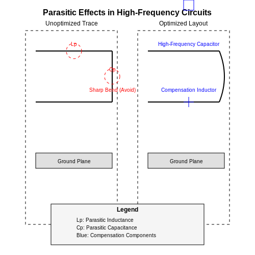
At high frequencies, parasitic inductance (Lp), capacitance (Cp), and resistance (Rp) arise from physical circuit structures. Trace geometry, component leads, and interconnects introduce stray reactances that deviate from ideal lumped-element models. For instance, a 10-mm PCB trace at 1 GHz can exhibit an inductive reactance of:
where L ≈ 8 nH/mm is the typical parasitic inductance of a microstrip trace.
Impact on Impedance Matching
Parasitics alter the effective impedance (Zeff) of matching networks. A nominally 50 Ω transmission line with 5 pF of shunt capacitance at 2 GHz introduces a susceptance (B) of:
This shifts the admittance (Y = 1/Z + jB), causing a 12% mismatch in a 50 Ω system. The resulting voltage standing wave ratio (VSWR) degrades to 1.3, increasing reflected power.
Mitigation Techniques
1. Layout Optimization
- Minimize trace lengths to reduce series inductance (Lp ∝ length).
- Use ground planes to lower loop inductance and parasitic capacitance.
- Avoid sharp bends in traces to prevent impedance discontinuities.
2. Component Selection
High-frequency capacitors (e.g., NP0/C0G dielectrics) exhibit lower parasitic inductance (ESL < 0.5 nH) compared to X7R ceramics. For inductors, planar or wirewound types with self-resonant frequencies (SRF) above the operating band are preferred:
3. Parasitic Cancellation
Stray capacitance can be compensated by adding series inductance (L = 1/(ω²Cp)). For a 3 pF parasitic capacitance at 5 GHz:
This is achievable via a short high-impedance transmission line segment (e.g., 100 Ω, 0.5 mm).
Case Study: RF Amplifier Matching
A 28 GHz power amplifier (PA) with 5 nH bondwire inductance requires compensation. A shunt capacitor (C = 1/(ω²L) ≈ 6.5 fF) is integrated into the matching network, improving power transfer efficiency from 78% to 92%.
3.3 PCB Layout and Transmission Line Effects
Transmission Line Fundamentals
At high frequencies, PCB traces behave as transmission lines rather than ideal conductors. The distributed inductance (L) and capacitance (C) per unit length dominate the impedance characteristics. The characteristic impedance (Z0) of a transmission line is given by:
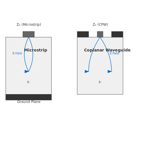
For microstrip traces (common in RF designs), Z0 depends on trace width (w), dielectric thickness (h), and substrate permittivity (εr). The Hammerstad-Jensen approximation provides an empirical solution:
where t is the trace thickness. Deviations beyond ±10% from the target impedance cause reflections, degrading signal integrity.
Critical Layout Considerations
Return Path Continuity: High-frequency currents follow the path of least inductance, not resistance. A broken return plane beneath a trace increases loop inductance, exacerbating crosstalk and EMI. For multilayer PCBs:
- Route critical signals adjacent to an unbroken ground plane
- Use via stitching to connect ground layers at λ/10 spacing
- Avoid slots or splits in reference planes under high-speed traces
Dispersion Effects: Above 1 GHz, the effective dielectric constant becomes frequency-dependent due to inhomogeneous field distribution in microstrips. This causes phase velocity variations, leading to signal distortion. Coplanar waveguide (CPW) structures mitigate this by confining fields more symmetrically.
Impedance Discontinuities and Mitigation
Common discontinuity sources include vias, bends, and component pads. A via’s parasitic inductance (Lvia) and capacitance (Cvia) create an effective impedance:
For a 0.3mm diameter via in FR4, typical values are Lvia ≈ 0.5 nH and Cvia ≈ 0.3 pF, yielding Zvia ≈ 40 Ω—a mismatch for 50 Ω lines. Countermeasures include:
- Back-drilling to remove unused via stubs
- Differential via pairs for balanced signals
- Ground return vias within λ/20 of signal vias
Material Selection Tradeoffs
Standard FR4 (εr ≈ 4.3) exhibits significant loss tangent (tan δ ≈ 0.02) above 5 GHz. Low-loss laminates like Rogers RO4003C (εr = 3.55, tan δ = 0.0027) reduce dielectric losses but increase cost. The attenuation constant (αd) due to dielectric loss is:
where c is the speed of light. At 10 GHz, FR4 suffers ≈ 0.7 dB/inch loss compared to 0.15 dB/inch for RO4003C.
4. Using Smith Charts for Design
4.1 Using Smith Charts for Design
The Smith Chart, developed by Phillip H. Smith in 1939, remains an indispensable tool for high-frequency impedance matching due to its ability to visualize complex impedances and admittances on a single normalized plane. At its core, the chart is a polar plot of the reflection coefficient Γ, where impedance transformations can be traced along constant resistance and reactance circles.
Normalization and Basic Properties
All impedances on the Smith Chart are normalized to a reference impedance Z0 (typically 50Ω or 75Ω). The normalized impedance z is defined as:
where r is the normalized resistance and x is the normalized reactance. The reflection coefficient Γ relates to z through:
The Smith Chart's key features include:
- Constant resistance circles: Centered along the real axis, shrinking toward the right side (open circuit at (1, 0)).
- Constant reactance arcs: Curves intersecting the real axis at (1, 0), representing inductive (upper half) or capacitive (lower half) components.
- VSWR circles: Concentric circles centered at the origin, with radii equal to |Γ|.
Impedance Matching Procedure
To match a load impedance ZL to Z0, follow these steps:
- Normalize the load impedance: Plot zL = ZL/Z0 on the chart.
- Add series components: Move along constant resistance circles for series inductors (clockwise) or capacitors (counterclockwise).
- Add shunt components: Convert to admittance (y = 1/z), then move along constant conductance circles for shunt capacitors (clockwise) or inductors (counterclockwise).
- Iterate until convergence: The goal is to reach the chart center (Γ = 0, perfect match).
Example: L-Section Matching
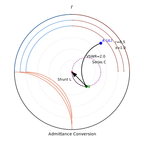
Consider matching ZL = 25 + j50Ω to 50Ω at 1 GHz. The normalized impedance is zL = 0.5 + j1.0:
- Plot zL at point A (intersection of r = 0.5 and x = 1.0 circles).
- Add series capacitance to cancel inductive reactance: Move along r = 0.5 to x = 0 (point B). The required reactance is -j1.0, yielding C = 1/(ω×1.0×Z0) ≈ 3.18 pF.
- Convert to admittance at point B (y = 2 + j0). Add shunt inductance to adjust conductance: Move along g = 2 to the center (y = 1 + j0). The required susceptance is -j1.0, giving L = Z0/(ω×1.0) ≈ 7.96 nH.
Advanced Techniques
For more complex matching networks, the Smith Chart enables:
- Stub matching: Using open or short-circuited transmission line segments (plotting along the chart's outer rim).
- Bandwidth analysis: Evaluating match quality across frequency by observing impedance locus movement.
- Noise matching: Optimizing for minimum noise figure rather than maximum power transfer by biasing toward specific Γopt points.
Modern vector network analyzers (VNAs) often overlay Smith Chart displays, allowing real-time impedance tuning. However, manual chart analysis remains valuable for developing intuition about matching network behavior under parameter variations.
4.2 Network Analyzer Measurements
Network analyzers are indispensable for characterizing high-frequency impedance matching networks, providing precise measurements of scattering parameters (S-parameters) across a wide frequency range. A vector network analyzer (VNA) measures both magnitude and phase of reflected and transmitted signals, enabling accurate extraction of impedance, admittance, and other RF parameters.
Calibration and Error Correction
Before measurements, a VNA must be calibrated to remove systematic errors introduced by cables, connectors, and fixtures. Common calibration methods include:
- Short-Open-Load-Thru (SOLT): Compensates for directivity, source match, and reflection tracking errors.
- Thru-Reflect-Line (TRL): Preferred for non-coaxial environments, such as on-wafer or waveguide measurements.
- Electronic Calibration (E-Cal): Uses a programmable impedance standard for rapid calibration.
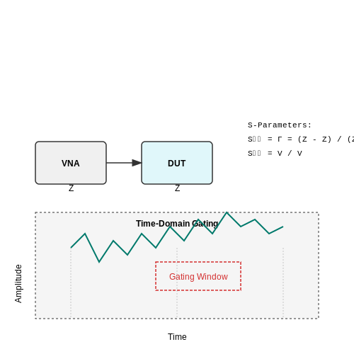
The corrected S-parameters relate to the impedance (Z) of the device under test (DUT) via:
where Z0 is the reference impedance (typically 50 Ω).
Measurement Techniques
For accurate impedance matching analysis, the following measurement approaches are critical:
One-Port Reflection Measurements
Used when only the input impedance is needed. The reflection coefficient (Γ) is derived from S11:
This is particularly useful for antenna tuning or filter design.
Two-Port Transmission Measurements
Essential for evaluating matching networks, amplifiers, or filters. The insertion loss (S21) and return loss (S11) are measured simultaneously. The impedance transformation ratio can be extracted from:
Time-Domain Gating
For multi-reflection environments (e.g., PCB traces with discontinuities), time-domain gating isolates the DUT response by windowing out unwanted reflections. The inverse Fourier transform converts frequency-domain data to time-domain, allowing selective gating before transforming back.
Practical Considerations
- Cable Phase Stability: Phase errors from cable movement can distort measurements; use phase-stable cables.
- Fixture De-embedding: Remove parasitic effects of test fixtures using known standards or electromagnetic simulation.
- Dynamic Range: Ensure the VNA’s dynamic range exceeds the DUT’s expected loss/gain.
Modern VNAs automate many of these processes, but understanding the underlying principles ensures correct interpretation of results.
4.3 Time-Domain Reflectometry (TDR)
Time-Domain Reflectometry (TDR) is a powerful technique for characterizing impedance discontinuities in transmission lines by analyzing reflected waveforms. A fast-rise-time step signal is injected into the transmission line, and the reflected voltage is measured as a function of time. The reflection coefficient Γ at any discontinuity is given by:
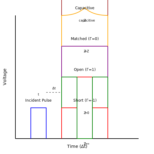
where ZL is the load impedance and Z0 is the characteristic impedance of the transmission line. The time delay Δt between the incident and reflected pulses determines the distance d to the discontinuity:
Here, vp is the propagation velocity of the signal in the transmission line, typically 60–80% of the speed of light in dielectric media. For a lossless line, vp is:
TDR Measurement Setup
A typical TDR system consists of:
- A high-bandwidth pulse generator with sub-nanosecond rise time.
- A sampling oscilloscope with ≥20 GHz bandwidth.
- Precision coaxial cables and connectors (e.g., 3.5 mm or SMA).
- Calibration standards (open, short, load) for reference.
Interpreting TDR Waveforms
The reflected waveform reveals key properties of impedance variations:
- Open circuit: Positive reflection (Γ = +1).
- Short circuit: Negative reflection (Γ = -1).
- Matched load: No reflection (Γ = 0).
- Capacitive discontinuity: Gradual positive slope.
- Inductive discontinuity: Gradual negative slope.
Applications in High-Frequency Systems
TDR is indispensable for:
- Locating faults in PCB traces and cables.
- Verifying impedance matching in RF circuits.
- Characterizing via stubs and connector transitions.
- Measuring dielectric constants of substrates.
Mathematical Derivation of TDR Resolution
The spatial resolution Δd of a TDR system is limited by the rise time tr of the incident pulse:
For a 35 ps rise-time pulse in a FR-4 PCB (vp ≈ 1.5×10⁸ m/s), the resolution is:
Higher bandwidth oscilloscopes and faster pulse generators improve resolution but increase cost and complexity.
5. Recommended Textbooks
5.1 Recommended Textbooks
- PDF High-Frequency Integrated Circuits - Cambridge University Press ... — 5 Circuit analysis techniques for high-frequency integrated circuits 318 5.1 Analog versus high-frequency circuit design 318 5.2 Impedance matching 321 5.3 Tuned circuit topologies and analysis techniques 335 5.4 Techniques to maximize bandwidth 342 5.5 Challenges in differential circuits at high frequency 356 5.6 Non-linear techniques 362 ...
- PDF Fundamentals of High-Frequency CMOS Analog Integrated Circuits — 3 High-frequency behavior of basic amplifiers 95 3.1 High-frequency behavior of a common-source amplifier 97 3.1.1 The R-C load case 99 3.2 The source follower amplifier at radio frequencies 103 3.3 The common-gate amplifier at high frequencies 110 3.4 The "cascode" amplifier 114 3.5 The CMOS inverter as a transimpedance amplifier 118
- PDF AN1275: Impedance Matching Network Architectures - Silicon Labs — dB is recommended because improving the S11 value further than -10 dB will only improve the mismatch loss by a minimal value i.e., the mismatch loss will be 0.13 dB or 0.04 dB when the S11 value is -15 dB or -20 dB respectively. AN1275: Impedance Matching Network Architectures Reflection Coefficient, VSWR, and Impedance Matching
- Impedance Matching Techniques - SpringerLink — Dutta Ray SC (2014) Triple frequency impedance matching by frequency transformation. IETE J Educ 55(1):47-51. Article Google Scholar Maktoomi MA, Hashmi MS, Yadav AP, Vishal K (2016) A generic tri-band matching network. IEEE Microwave Wireless Compon Lett 26(5):337-339. Google Scholar
- PDF Chapter 5 - Impedance Matching and Tuning - University of Kansas — 3/25/2009 section 5_1 Matching with Lumped Elements 1/3 Jim Stiles The Univ. of Kansas Dept. of EECS Chapter 5 - Impedance Matching and Tuning One of the most important and fundamental two-port networks that microwave engineers design is a lossless matching network (otherwise known as an impedance transformer). HO: MATCHING NETWORKS
- 5 Impedance Matching - Springer — When the generator impedance is complex, as in figure 5.1b, maximum current is obtained for any value of R 1 by making X 1 = -X g• so that the reactances cancel. This reduces the circuit to that in figure 5.la, with maximum power transfer occurring when the load impedance is the complex conjugate of the generator impedance, Z 1 = (Rg-jX g ...
- Antenna Impedance Measurement and Matching - Texas Instruments — 3 Evaluation Board Matching Components Location. In high frequency electronics, standard values of impedance are 50, 75, and 100 Ohm. Most manufacturers of test equipment, cables, connectors, and antennas use these values. Transceiver data sheets or evaluation board schematics usually have a matching circuit for transforming a non-value. www.ti.com
- Impedance matching (Chapter 5) - A Practical Introduction to Electronic ... — For example, the input impedance of a 12 V light bulb rated at 0.5 A is 12/ 0.5Ω, or 24 Ω. The bulb is a clear example of impedance because we know that there is nothing but a filament to consider. The input impedance of a circuit such as bipolar transistor amplifier might seem to be more complicated.
- PDF IMPEDANCE MATCHING: - Electronic Design — Impedance Matching. The common problem of mismatched load and source impedances can be corrected by . connecting an impedance-matching device between source and load (Fig. 8). The imped-ance (Z) matching device may be a component, circuit, or piece of equipment. 8. An impedance-matching circuit or component makes the load match the generator ...
- Transmission Lines and Impedance Matching Techniques — Transmission Lines and Impedance Matching Techniques 5.1 INTRODUCTION. At low RF frequencies, a wire or a line on a printed circuit board can be used to connect two electronic components. At high RF or microwave frequencies, the wire becomes lossy, radiates power, and has significant reactance and is difficult to model accurately.
5.2 Key Research Papers
- Impedance Matching Techniques - SpringerLink — Optimum impedance matching over a broad frequency band is the key in design of any broadband RF circuit and system. To match a frequency-dependent source impedance, for maximum power transfer, the realized load impedance also should vary with the frequency to ensure the complex conjugate load impedance to the source impedance across the full ...
- Research on the Impedance Matching Technology of the Transmission Line ... — Impedance matching technology is the key to designing high-frequency electronic circuits. In order to solve the problem of impedance matching of transmission lines with special structures, the ...
- Broadband impedance matching design method for dipole acoustic logging ... — Using the half-power point as a reference, after impedance matching, the frequency bandwidth of the transducer increases from 4.1-4.5 kHz (0.4 kHz) to 4-5.2 kHz (1.2 kHz), the working bandwidth of the transducer widens three times, and the average active power in the band increases 2.3 times.
- PDF AN1275: Impedance Matching Network Architectures - Silicon Labs — cuit is frequency-dependent, the perfect impedance match between the source and the load will also occur at a particular frequency. The frequency band over which the impedance is matched can be determined by the value of the "Q" factor of the matching network, which depends on the network architecture. B W = F Q Where: BW = -3 dB Bandwidth
- Design of a Highly Efficient Wideband Multi-Frequency Ambient RF Energy ... — The impedance matching depends on the specifically designed frequency bands, whenever the source and load is a reactive component. Thus, the RF bandpass filter section is considered as an impedance matching network. In , it was demonstrated that the most frequently used RF filters (as an impedance matching network) are L, π and T, respectively ...
- PDF Designing Impedance Matching Networks for Rf and Microwave Devices and ... — Chapter 2 contains background and related works associated with impedance matching. In this section some devices in which impedance matching is a must requirement such as Low Noise Amplifier, Power Dividers, Antenna Feed lines etc. are discussed briefly. Chapter 3 discuss about High Impedance Transforming Dual-Band Wilkinson Power
- Compact high-efficiency broadband/multi-band stacked back-to-back high ... — A compact broadband high-efficiency rectenna is proposed. It is based on a wideband rectification circuit with a fourth-order bandpass filter impedance matching transformer. The rectifier has a PCE of higher than 50% in the frequency range of 4.9 to 6.1 GHz at an input power level from −4 to 10 dBm. The maximum measured PCE is 73.57 % at 10 dBm.
- A Distributed Triband Impedance Matching Network Based on Multiresonant ... — In this paper, the design, implementation and evaluation of a concurrent distributed triband impedance matching network for operation at 2.4 GHz (Bluetooth), 3.7 GHz (WiFi) and 5.2 GHz (WiFi) are presented. The measurement results show that the reflection coefficients obtained are less than -14 dB with maximum insertion loss of 1.4 dB.
- (PDF) A Methodology Improving Off-Chip, Lumped RF Impedance Matching ... — Impedance matching is concurrent with any radio frequency (RF) circuit design and is essential for maximizing the gain and efficiency while minimizing the noise of high-frequency amplifiers as ...
- Piezoelectric energy harvester impedance matching using a piezoelectric ... — In [5], the DCM flyback converter and in [4], the DCM buck-boost converter is used for resistive impedance matching.The switching frequency in the DCM dc-dc converter is kept low to reduce the switching losses. To reduce the wire resistance losses in the magnetic components of these converters, thicker wires are used which results in large size inductor and transformer.
5.3 Online Resources and Tools
- PDF High-Frequency Integrated Circuits - Cambridge University Press ... — 5 Circuit analysis techniques for high-frequency integrated circuits 318 5.1 Analog versus high-frequency circuit design 318 5.2 Impedance matching 321 5.3 Tuned circuit topologies and analysis techniques 335 5.4 Techniques to maximize bandwidth 342 5.5 Challenges in differential circuits at high frequency 356 5.6 Non-linear techniques 362 ...
- PDF Fundamentals of High-Frequency CMOS Analog Integrated Circuits — 3 High-frequency behavior of basic amplifiers 95 3.1 High-frequency behavior of a common-source amplifier 97 3.1.1 The R-C load case 99 3.2 The source follower amplifier at radio frequencies 103 3.3 The common-gate amplifier at high frequencies 110 3.4 The "cascode" amplifier 114 3.5 The CMOS inverter as a transimpedance amplifier 118
- Impedance Matching Techniques - SpringerLink — Optimum impedance matching over a broad frequency band is the key in design of any broadband RF circuit and system. To match a frequency-dependent source impedance, for maximum power transfer, the realized load impedance also should vary with the frequency to ensure the complex conjugate load impedance to the source impedance across the full frequency band.
- Antenna Impedance Measurement and Matching - Texas Instruments — 3 Evaluation Board Matching Components Location. In high frequency electronics, standard values of impedance are 50, 75, and 100 Ohm. Most manufacturers of test equipment, cables, connectors, and antennas use these values. Transceiver data sheets or evaluation board schematics usually have a matching circuit for transforming a non-value. www.ti.com
- PDF AN1275: Impedance Matching Network Architectures - Silicon Labs — cuit is frequency-dependent, the perfect impedance match between the source and the load will also occur at a particular frequency. The frequency band over which the impedance is matched can be determined by the value of the "Q" factor of the matching network, which depends on the network architecture. B W = F Q Where: BW = -3 dB Bandwidth
- PDF Chapter 5 Impedance matching and tuning - 國立臺灣大學 — •Impedance matching concept given ZL, design a matching network to have in=0 or selected value matching Z o network in L Z L Discussion 1. Matching network usually uses lossless components: L, C, transmission line and transformer. 2. There are possible solutions for the matching circuit. 3. Properly use Smith chart to find the optimal design. 4.
- PDF Understanding the Relevance of Harmonic Impedance Matching in Amplifi ... — overall frequency range, and the matching net-work synthesized to achieve the desired wide-band response. In this case, it is entirely pos-sible that the harmonic frequencies (2fo, 3fo…) of the lower frequency band overlap a funda-mental frequency in the middle or upper por-112 MICROWAVE JOURNAL APRIL 2015 TechnicalFeature Scan page
- PDF AN721: Impedance Matching Networks Applied to RF Power Transistors - MACOM — IMPEDANCE MATCHING NETWORKS APPLIED TO RF POWER TRANSISTORS Prepared by: B. Becciolini 1. INTRODUCTION Some graphic and numerical methods of impedance matching will be reviewed here. The examples given will refer to high frequency power amplifiers. Although matching networks normally take the form of filters and therefore are also useful to ...
- PDF Chapter. 5 Impedance Matching and Tuning - 통합홈페이지 관리 ... — Impedance matching in a power distribution network (such as an antenna array feed network) will reduce amplitude and phase errors. FIGURE 5.1. A lossless network matching an arbitrary load impedance to a transmission line. - Factors that may be important in the selection of a particular matching network: 1) Complexity: simple
- High-Frequency Circuit Design - SpringerLink — This chapter therefore discusses the basics of impedance matching, resonators, and matching networks which are crucial in RF circuit design. Then, the two primary building blocks for high-frequency amplifiers above 100 GHz in this book are detailed: the neutralized pseudo-differential pair and transformer-based matching network.