High-Frequency Circuit Design Techniques
1. Characteristics of High-Frequency Signals
1.1 Characteristics of High-Frequency Signals
Wave Propagation and Skin Effect
At high frequencies (typically above 100 MHz), electromagnetic wave propagation dominates over lumped-element behavior. The skin effect becomes significant, causing current to concentrate near the surface of conductors. The skin depth (δ) is given by:
where ρ is resistivity, ω is angular frequency, and μ is permeability. For copper at 1 GHz, δ ≈ 2.1 μm, drastically increasing conductor loss compared to DC conditions.
Transmission Line Behavior
When signal wavelengths approach conductor dimensions (λ ≈ trace length), transmission line theory must replace conventional circuit analysis. The characteristic impedance (Z0) of a microstrip line depends on its geometry:
where h is substrate height, w is trace width, t is trace thickness, and ϵr is relative permittivity. Mismatches cause reflections quantified by the reflection coefficient Γ:
Dielectric Loss and Dispersion
High-frequency substrates exhibit frequency-dependent loss tangent (tanδ) and permittivity. The attenuation constant (αd) due to dielectric loss is:
where f is frequency, c is light speed, and ϵreff is effective permittivity. FR4 (tanδ ≈ 0.02) becomes impractical above 5 GHz, necessitating low-loss materials like Rogers RO4003C (tanδ ≈ 0.0027).
Parasitic Effects
Discrete components exhibit non-ideal behavior:
- Capacitors: Equivalent series inductance (ESL) creates self-resonance (typically 10-100 MHz for SMD ceramics)
- Inductors: Parasitic capacitance limits usable frequency range
- Transistors: Package lead inductance (~1 nH/mm) affects gain and stability
The Smith Chart becomes essential for impedance matching, visualizing how load impedance varies with frequency due to these parasitics.
Noise Considerations
Thermal noise power spectral density remains flat (4kTB), but active devices show increasing noise figure (NF) with frequency due to:
- Transit time effects in semiconductors
- Lossy substrate coupling
- Radiation losses in interconnects
Phase noise in oscillators follows Leeson's model:
where fm is offset frequency, f0 is carrier frequency, QL is loaded Q-factor, and fc is flicker noise corner.
1.2 Transmission Line Theory
Fundamentals of Transmission Lines
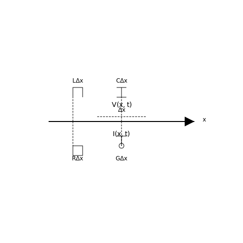
At high frequencies, conductors no longer behave as ideal short circuits but instead exhibit distributed impedance characteristics. A transmission line is modeled as a series of infinitesimal segments, each contributing inductance (L), capacitance (C), resistance (R), and conductance (G) per unit length. The telegrapher's equations describe voltage (V) and current (I) propagation:
For lossless lines (R = G = 0), these reduce to wave equations with propagation velocity v = 1/√(LC).
Characteristic Impedance
The characteristic impedance (Z0) is a fundamental property of a transmission line, defined as the ratio of voltage to current in a traveling wave:
For lossless lines, this simplifies to Z0 = √(L/C). Common values range from 50 Ω (RF systems) to 75 Ω (cable TV). Mismatches cause reflections quantified by the reflection coefficient (Γ):
Propagation Constant and Dispersion
The propagation constant (γ) characterizes signal attenuation and phase shift:
where α is the attenuation constant (Np/m) and β is the phase constant (rad/m). In dielectric media, dispersion occurs when β varies nonlinearly with frequency, causing signal distortion.
Termination and Matching Techniques
Proper termination prevents reflections. Key methods include:
- Resistive termination: Matches Z0 exactly at load
- Quarter-wave transformer: Uses λ/4 line to match impedances via Z1 = √(Z0ZL)
- Stub matching: Reactive elements cancel reflections at specific frequencies
Microstrip and Stripline Design
Printed circuit board transmission lines require precise geometry control. Microstrip impedance depends on trace width (w), substrate height (h), and relative permittivity (εr):
Stripline (embedded traces) offers better shielding but lower impedance range. Modern RF designs use 3D EM solvers to account for fringing fields and discontinuities.
Time-Domain Reflectometry (TDR)
TDR measures impedance variations by analyzing reflected step responses. The round-trip delay (Δt) locates faults at distance d = vΔt/2, where v is the propagation velocity. High-speed digital systems use TDR for signal integrity validation.
1.3 Skin Effect and Proximity Effect
Skin Effect: Current Crowding at High Frequencies
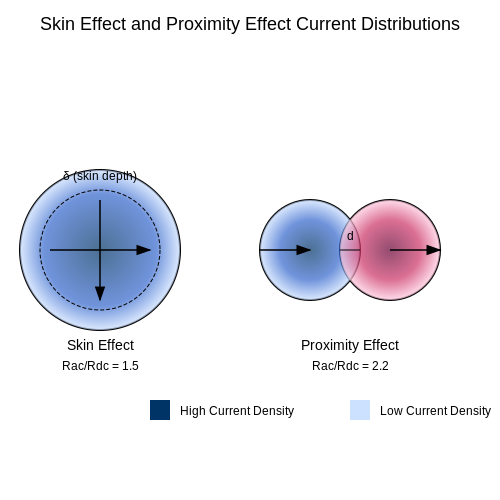
At DC or low frequencies, current distributes uniformly across a conductor's cross-section. However, as frequency increases, time-varying magnetic fields induce eddy currents that oppose the flow of charge carriers, forcing current toward the conductor's outer surface. This phenomenon, known as the skin effect, increases effective resistance and reduces usable conductor area.
The skin depth (δ), defined as the depth at which current density decays to 1/e (≈37%) of its surface value, is derived from Maxwell's equations for a semi-infinite plane conductor:
where ω is angular frequency, μ is permeability, σ is conductivity, ρ is resistivity, and f is frequency. For copper at 20°C (ρ = 1.68×10⁻⁸ Ω·m, μ ≈ μ₀ = 4π×10⁻⁷ H/m), skin depth simplifies to:
At 1 GHz, δ ≈ 2.1 μm—meaning most current flows within a thin surface layer. The AC resistance Rac of a round wire with radius a ≫ δ becomes:
Proximity Effect: Conductor Interaction
The proximity effect further exacerbates losses when multiple conductors carry time-varying currents in close proximity. Adjacent magnetic fields induce circulating currents that distort current distribution, concentrating charge flow in regions farthest from neighboring conductors. In parallel busbars or transformer windings, this can double effective resistance compared to isolated skin effect predictions.
For two identical parallel conductors carrying opposing currents (e.g., differential pairs), the power loss per unit length P' is:
where d is center-to-center spacing. The second term represents proximity-induced losses, dominating when d < 2a.
Mitigation Techniques
- Litz wire: Multiple insulated strands woven in a precise pattern to average skin and proximity effects across frequencies.
- Planar conductors: Wide, thin traces minimize unused cross-sectional area in PCBs.
- Surface treatments: Silver plating (higher conductivity than copper) reduces resistive losses.
- Geometric spacing: Maintaining d > 3a between high-current conductors minimizes proximity coupling.
Practical Implications
In RF amplifiers above 10 MHz, skin effect necessitates hollow or silver-plated waveguides. Power electronics operating at 100s of kHz (e.g., switch-mode supplies) require careful winding layouts to avoid proximity-induced heating in transformers. High-speed digital interconnects (>1 GHz) use controlled impedance microstrips with calculated dielectric losses accounting for surface roughness.
2. High-Frequency Resistors and Capacitors
2.1 High-Frequency Resistors and Capacitors
Parasitic Effects in High-Frequency Components
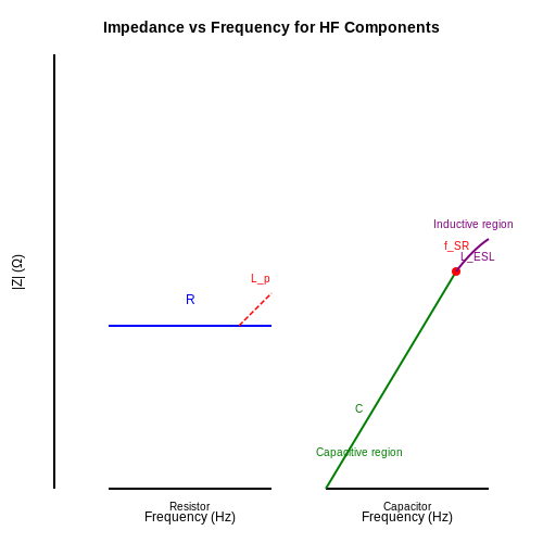
At high frequencies, resistors and capacitors exhibit non-ideal behavior due to parasitic inductance (Lp) and capacitance (Cp). A resistor’s impedance deviates from its DC value as frequency increases, modeled by:
where ω = 2πf. The self-resonant frequency (fSR) marks the point where inductive and capacitive reactances cancel:
Above fSR, the resistor behaves inductively. For example, a 1 kΩ thin-film resistor with Lp = 0.5 nH and Cp = 0.2 pF resonates at ~16 GHz.
Capacitor Frequency Response
Capacitors follow a similar impedance curve:
LESL (equivalent series inductance) and RESR (equivalent series resistance) dominate at high frequencies. Multilayer ceramic capacitors (MLCCs) minimize LESL through interdigitated electrodes, achieving fSR values up to 10 GHz for 0402 packages.
Material Considerations
Resistors:
- Thin-film (NiCr, TaN): Low Lp (~0.1–1 nH), stable up to 20 GHz.
- Thick-film: Higher parasitics, limited to ~1 GHz.
Capacitors:
- Class I ceramics (C0G/NP0): Minimal dielectric losses (tan δ < 0.001), suited for RF matching.
- Class II (X7R, Y5V): Higher permittivity but nonlinear with voltage/temperature.
Layout Mitigation Techniques
To suppress parasitics in PCB designs:
- Use 0201/0402 packages for reduced lead inductance.
- Place ground vias adjacent to capacitor pads to minimize loop area.
- Route differential pairs symmetrically to balance parasitic capacitance.
High-Frequency Q Factor
The quality factor Q quantifies energy loss in reactive components. For a capacitor:
For a series RLC network (e.g., a capacitor with parasitics), the system Q is:
High-Q designs (>100 at 1 GHz) require low-loss materials like fused silica or alumina substrates.
Inductors and Transformers at High Frequencies
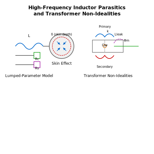
Parasitic Effects in High-Frequency Inductors
At high frequencies, inductors exhibit parasitic effects that deviate from ideal behavior. The primary non-idealities include:
- Parasitic capacitance (Cp) – Stray capacitance between windings, modeled as a parallel element.
- Series resistance (Rs) – Ohmic losses due to wire resistance and skin effect.
- Core losses (Rc) – Hysteresis and eddy current losses in magnetic materials.
The impedance of a real inductor is given by:
where ω is the angular frequency. The self-resonant frequency (SRF) occurs when the inductive and capacitive reactances cancel:
Beyond SRF, the inductor behaves capacitively, rendering it ineffective for energy storage.
Skin and Proximity Effects
At high frequencies, current density becomes non-uniform across conductors due to:
- Skin effect – Current crowds near the conductor surface, increasing effective resistance.
- Proximity effect – Adjacent windings induce opposing eddy currents, further raising losses.
The skin depth δ is derived from Maxwell’s equations:
where ρ is resistivity and μ is permeability. For copper at 1 GHz, δ ≈ 2.1 µm, necessitating litz wire or thin-film geometries.
High-Frequency Transformer Design
Transformers face additional challenges at high frequencies:
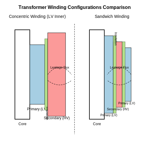
- Leakage inductance (Lleak) – Flux not coupling both windings, causing voltage spikes.
- Interwinding capacitance (Ciw) – Capacitive coupling between primary and secondary.
The coupling coefficient k quantifies efficiency:
where M is mutual inductance. Ferrite cores with high permeability are preferred to minimize losses, but their frequency response must be characterized to avoid saturation.
Practical Mitigation Techniques
To optimize performance:
- Use distributed air-core inductors for minimal Cp in RF circuits.
- Employ planar transformers with PCB windings to control parasitics.
- Implement resonant topologies (e.g., LLC converters) to exploit parasitics beneficially.
2.3 Parasitic Effects and Mitigation
Parasitic Capacitance in High-Frequency Circuits
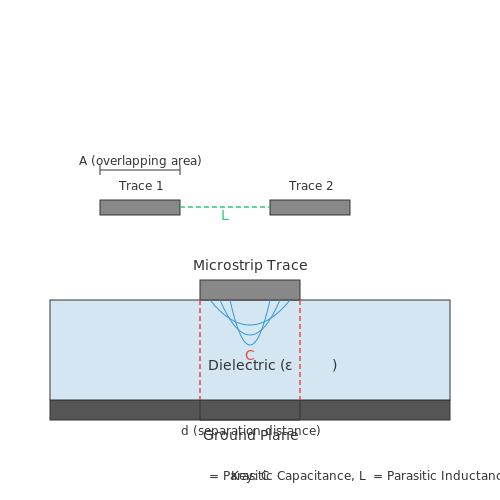
At high frequencies, unintended capacitance arises between conductors, traces, and ground planes due to electric field coupling. For parallel plates separated by a dielectric, the parasitic capacitance \(C_p\) is given by:
where \(\epsilon_r\) is the relative permittivity, \(\epsilon_0\) is the vacuum permittivity, \(A\) is the overlapping area, and \(d\) is the separation distance. In PCB traces, this manifests as:
- Trace-to-ground capacitance: Dominates in microstrip lines, increasing propagation delay.
- Intertrace coupling: Causes crosstalk in densely routed designs.
Parasitic Inductance and Its Impact
Even short conductor segments exhibit inductance at RF frequencies. The partial self-inductance \(L_p\) of a wire with length \(l\) and radius \(r\) is:
This becomes critical in:
- Ground bounce: Inductive voltage drops in ground paths disrupt reference planes.
- Impedance mismatches: Degrades signal integrity in transmission lines.
Mitigation Strategies
1. Layout Optimization
Minimize parasitic capacitance by:
- Reducing parallel trace lengths (< 1/20th of the wavelength).
- Using guard rings or ground shields around sensitive nodes.
2. Controlled Impedance Design
For transmission lines, maintain characteristic impedance \(Z_0\) by solving:
where \(L'\) and \(C'\) are per-unit-length inductance and capacitance. Use Rogers substrates for stable \(\epsilon_r\) at GHz frequencies.
3. Decoupling Techniques
Place high-frequency decoupling capacitors (e.g., 0402 MLCCs) with loop inductance \(L_{loop}\) minimized:
where \(h\) is height above ground, \(l\) is trace length, and \(w\) is trace width. Place capacitors < 1mm from IC power pins.
Case Study: GHz Oscillator Stability
In a 5 GHz VCO, parasitic capacitance from bond wires (~0.5 nH/mm) shifted the tuning curve by 12%. Mitigation involved:
- Flip-chip bonding to eliminate wires.
- On-die MIM capacitors for stable \(C\).
3. Transistor Selection for High-Frequency Applications
3.1 Transistor Selection for High-Frequency Applications
Key Performance Metrics
The selection of transistors for high-frequency circuits hinges on several critical parameters. The transition frequency (fT) defines the frequency at which the current gain drops to unity, while the maximum oscillation frequency (fmax) indicates the frequency where power gain equals one. These are derived from small-signal models:
where gm is transconductance, Cgs and Cgd are parasitic capacitances, and Rg is gate resistance. For RF applications, fmax often matters more than fT due to its direct correlation with power gain roll-off.
Transistor Technologies Compared
Different semiconductor technologies offer trade-offs in high-frequency performance:
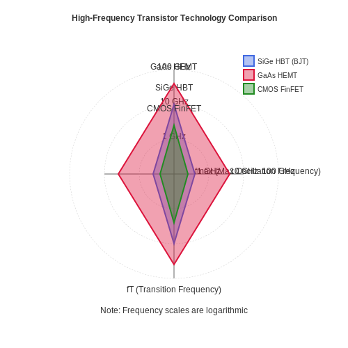
- Silicon Bipolar Junction Transistors (BJTs): Historically dominant, with fT up to 300 GHz in SiGe HBTs. Their high current drive suits power amplifiers but suffers from higher noise figures.
- GaAs HEMTs: Provide fmax exceeding 1 THz due to high electron mobility. Ideal for low-noise amplifiers (LNAs) in mmWave systems.
- CMOS (Nanoscale Nodes): Modern 22 nm FinFETs achieve fT > 400 GHz, but substrate losses and flicker noise limit dynamic range.
Parasitic Considerations
At high frequencies, parasitic elements dominate performance. A transistor’s input impedance (Zin) becomes capacitive:
where Ls is source inductance. Package parasitics (e.g., bond wire inductance ~0.5 nH/mm) can detune matching networks, necessitating electromagnetic (EM) simulation during layout.
Noise Optimization
The noise figure (NF) is minimized when the source impedance matches the transistor’s optimum noise impedance (Γopt). For a FET, the Fukui equation approximates NFmin:
Low-noise designs often bias transistors below peak fT to reduce thermal noise contributions.
Case Study: 60 GHz PA Design
A 60 GHz power amplifier in 45 nm SOI CMOS achieves 18 dBm output power by stacking transistors to overcome breakdown voltage limits. The gate periphery is scaled to balance gain (Gmax) and efficiency:
Interstage matching uses slow-wave coplanar waveguides to mitigate dielectric losses.
3.2 Amplifier Topologies for RF Circuits
Common-Emitter and Common-Source Amplifiers
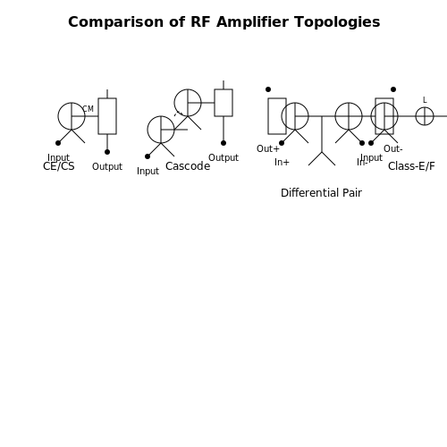
The common-emitter (CE) and common-source (CS) configurations are widely used in RF amplifiers due to their high gain and moderate input/output impedance characteristics. For a bipolar junction transistor (BJT) in CE configuration, the small-signal voltage gain \(A_v\) is derived as:
where \(g_m\) is the transconductance and \(R_L\) is the load resistance. For a MOSFET in CS configuration, the gain follows a similar form but with a different transconductance expression:
These topologies suffer from the Miller effect at high frequencies, which increases the effective input capacitance and reduces bandwidth. Neutralization techniques or cascode configurations are often employed to mitigate this.
Cascode Amplifiers
The cascode topology combines a CE/CS stage with a common-base (CB) or common-gate (CG) stage to improve bandwidth and gain stability. The cascode structure reduces the Miller effect by isolating the input and output capacitances. The overall gain is:
where \(r_{o1}\) and \(r_{o2}\) are the output resistances of the two transistors. This configuration is prevalent in low-noise amplifiers (LNAs) and RF front-ends due to its superior linearity and power handling.
Differential Pair Amplifiers
Differential amplifiers, using BJTs or MOSFETs in a long-tailed pair configuration, are essential for rejecting common-mode noise in RF systems. The differential gain \(A_{diff}\) is:
where \(R_C\) is the collector (or drain) resistance and \(r_o\) is the transistor output resistance. Modern RF integrated circuits (ICs) often use active loads (e.g., current mirrors) to enhance gain while maintaining a compact layout.
Distributed Amplifiers
For ultra-wideband applications, distributed amplifiers employ transmission lines to combine the gains of multiple stages while maintaining a flat frequency response. The gain-bandwidth product (GBW) is theoretically unlimited, but practical constraints arise from losses and phase matching. The effective gain per stage is:
where \(n\) is the number of stages, \(g_m\) is the transconductance, and \(Z_0\) is the characteristic impedance of the transmission line. This topology is common in microwave monolithic integrated circuits (MMICs).
Class-E and Class-F Power Amplifiers
Switching-mode amplifiers (Class-E, Class-F) achieve high efficiency (\(>90\%\)) by operating transistors in saturation. Class-E amplifiers use a tuned LC network to shape voltage and current waveforms, minimizing overlap losses. The output power \(P_{out}\) is:
Class-F amplifiers further improve efficiency by harmonic tuning, creating square-wave voltage and half-sine current waveforms. These are critical in 5G and radar systems where power efficiency is paramount.
3.3 Noise Figure and Linearity Considerations
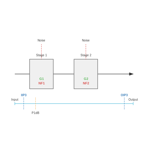
In high-frequency circuit design, noise and linearity are critical performance metrics that directly impact signal integrity and system sensitivity. The noise figure (NF) quantifies the degradation in signal-to-noise ratio (SNR) as a signal passes through a component or system, while linearity determines the ability to handle large signals without distortion.
Noise Figure Fundamentals
The noise figure is defined as the ratio of the input SNR to the output SNR, expressed in decibels (dB):
For a cascaded system with n stages, the total noise figure NFtotal is given by Friis' formula:
where NFi and Gi are the noise figure and gain of the i-th stage, respectively. This highlights the importance of the first stage's noise performance in receiver design.
Linearity Metrics
Linearity is characterized by several key parameters:
- 1-dB Compression Point (P1dB): The input power level where the gain drops by 1 dB from its linear value.
- Third-Order Intercept Point (IP3): The theoretical point where third-order intermodulation products would equal the fundamental tones.
The relationship between input and output IP3 (IIP3 and OIP3) is given by:
where G is the gain in dB. For cascaded stages, the total IIP3 can be approximated by:
Trade-offs Between Noise and Linearity
In practice, optimizing for low noise figure often compromises linearity, and vice versa. For example:
- Low-noise amplifiers (LNAs) are typically biased for minimum NF, which reduces IP3.
- Power amplifiers prioritize linearity at the expense of higher noise contribution.
The dynamic range of a system is bounded by the noise floor at the lower end and the compression point at the upper end. The spurious-free dynamic range (SFDR) is particularly important in communication systems:
where Nfloor is the system noise floor in dBm.
Practical Design Techniques
Several methods can improve noise and linearity performance:
- Impedance Matching: Optimal source impedance minimizes NF while maintaining stability.
- Feedback Techniques: Negative feedback can improve linearity at the cost of reduced gain.
- Device Selection: GaAs and InP HEMTs offer superior noise performance compared to Si-based devices at microwave frequencies.
Modern circuit simulators allow co-optimization of noise and linearity through load-pull and noise-pull simulations, enabling designers to find the best compromise for a given application.
4. Smith Chart Techniques
4.1 Smith Chart Techniques
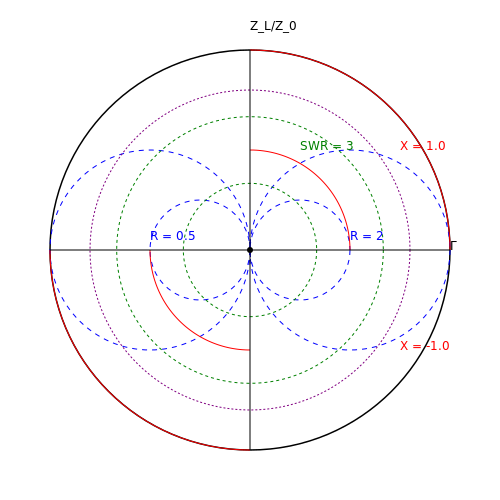
The Smith Chart, developed by Phillip H. Smith in 1939, remains an indispensable tool for solving transmission line and impedance matching problems at high frequencies. Its polar representation of complex impedances simplifies the visualization of reflection coefficients, standing wave ratios (SWR), and impedance transformations.
Mathematical Foundation
The Smith Chart is derived from the reflection coefficient Γ, defined as:
where ZL is the load impedance and Z0 is the characteristic impedance of the transmission line. The chart maps normalized impedances (z = ZL/Z0) onto a unit circle in the complex Γ-plane.
Key Features of the Smith Chart
- Constant Resistance Circles: Represent loci of constant real part of impedance.
- Constant Reactance Arcs: Represent loci of constant imaginary part of impedance.
- SWR Circles: Concentric circles centered at the origin, indicating constant standing wave ratio.
- Admittance Coordinates: Dual representation enabling easy conversion between impedance and admittance.
Practical Applications
Impedance Matching
Single-stub matching networks can be designed by:
- Locating the load impedance on the chart.
- Moving along a constant SWR circle to intersect the desired matching point.
- Calculating the required stub length and position.
where Δθ is the angular rotation on the Smith Chart and λ is the wavelength.
Noise Figure Optimization
For low-noise amplifier design, the Smith Chart helps identify optimal source impedance regions that minimize noise figure while maintaining acceptable gain.
Advanced Techniques
Multi-element Matching: Cascaded LC networks can be designed by successive impedance transformations along constant conductance or resistance circles.
Broadband Matching: The bandwidth of matching networks can be visualized by plotting frequency-dependent impedance trajectories on the Smith Chart.
Computer-Aided Smith Chart Analysis
Modern vector network analyzers (VNAs) display real-time Smith Chart representations, enabling:
- Interactive tuning of matching networks
- Visualization of component parasitics
- Stability analysis through Γin and Γout plots
The following SVG diagram illustrates a typical Smith Chart with key features labeled:
4.2 Lumped and Distributed Matching Networks
Matching networks are essential in high-frequency circuit design to ensure maximum power transfer between components with mismatched impedances. The choice between lumped and distributed matching techniques depends on frequency, physical constraints, and performance requirements.
Lumped Element Matching
Lumped matching networks use discrete capacitors and inductors to transform impedances. These networks are effective at frequencies where the physical size of components is much smaller than the wavelength (λ). The most common topologies include:
- L-section – Simplest two-component network, but limited to specific impedance ranges.
- Pi (π) and T-networks – Provide greater flexibility and wider matching ranges.
- High-Q networks – Employ resonant structures for narrowband applications.
The impedance transformation for an L-section can be derived from the following equations. For a series-L, shunt-C network:
Solving for matching conditions (Zin = Z0) yields:
Distributed Matching Networks
At microwave frequencies (f > 1 GHz), distributed elements (transmission lines) replace lumped components due to parasitic effects. Key approaches include:
- Quarter-wave transformer – A λ/4 transmission line section with characteristic impedance Z1 = √(Z0ZL).
- Stub matching – Uses open or short-circuited transmission line segments to cancel reactance.
- Tapered lines – Provide broadband matching via gradual impedance transitions.
The quarter-wave transformer’s bandwidth is limited by its length dependency. The fractional bandwidth (Δf/f0) is approximated by:
where Γm is the maximum tolerable reflection coefficient.
Hybrid Matching Techniques
For wideband or multi-frequency applications, hybrid networks combine lumped and distributed elements. Examples include:
- LC-loaded transmission lines – Enhance bandwidth by introducing resonances.
- Stepped-impedance networks – Use cascaded sections of varying impedances.
Practical implementations must account for:
- Parasitic inductance/capacitance in lumped elements at high frequencies.
- Dielectric and conductor losses in transmission lines.
- Manufacturing tolerances affecting performance.
4.3 Bandpass and Lowpass Filter Design
Fundamentals of Filter Transfer Functions
The frequency response of bandpass and lowpass filters is governed by their transfer function H(s), where s = σ + jω. For a second-order lowpass filter:
where ω0 is the cutoff frequency (rad/s) and Q is the quality factor. The bandpass equivalent is:
Pole-Zero Analysis and Topology Selection
Butterworth filters provide maximally flat passbands, while Chebyshev designs trade ripple for steeper roll-off. For a Butterworth lowpass prototype:
where n is the order. Component values for ladder networks derive from g-parameters:
Active Filter Implementation
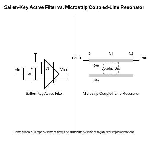
Sallen-Key topologies are prevalent for active implementations. The gain K and Q for a lowpass variant are:
Microstrip Bandpass Filters
At RF frequencies, coupled-line resonators implement bandpass behavior. The coupling coefficient β between λ/4 resonators is:
where Z0e and Z0o are even/odd mode impedances. Fractional bandwidth relates to Qext:
Practical Design Considerations
- Component tolerances: 1% resistors and NP0/C0G capacitors minimize shift in f0
- Parasitics: PCB pad capacitance (~0.2pF) affects high-Q designs above 100MHz
- Dynamic range: Op-amp slew rate must exceed 2πf0Vpk
Measurement and Tuning
Network analyzer measurements should account for fixture de-embedding. For a 50Ω system:
Tuning involves iterative adjustment of resonator gaps (for microstrip) or capacitor banks (for lumped-element).
5. Grounding and Shielding Techniques
5.1 Grounding and Shielding Techniques
Grounding Strategies for High-Frequency Circuits
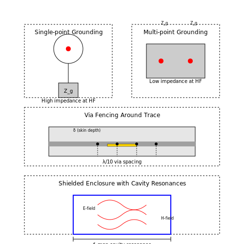
In high-frequency circuits, improper grounding introduces parasitic inductance and capacitance, leading to signal integrity degradation. A single-point ground is effective at low frequencies but fails above a few MHz due to ground loop currents. Instead, a multi-point grounding system minimizes loop area by connecting ground returns at multiple locations, reducing impedance at RF frequencies. The ground plane impedance is given by:
where μ0 is the permeability of free space, σ is the conductivity of the ground plane material, and ϵ is the permittivity. For frequencies above 10 MHz, a continuous ground plane (typically copper with ≥1 oz/ft² thickness) becomes essential to maintain low impedance.
Shielding Against Electromagnetic Interference
Effective shielding requires both electric field (E-field) and magnetic field (H-field) containment. For E-fields, thin conductive enclosures (≥1 skin depth) provide sufficient attenuation. The skin depth δ is calculated as:
For H-field shielding at high frequencies, high-permeability materials (e.g., mu-metal) are used in combination with conductive layers. The shielding effectiveness (SE) in dB for a conductive barrier is:
where A is absorption loss, R is reflection loss, and K accounts for multiple reflections.
Practical Implementation Techniques
- Partitioned Ground Planes: Separate analog, digital, and RF grounds with strategic connections at a single point near power entry
- Via Fencing: Surround sensitive traces with grounded vias spaced at λ/10 to suppress surface wave propagation
- Gasketed Enclosures: Use conductive elastomers or finger stock to maintain continuous shielding at enclosure seams
Common Pitfalls in High-Frequency Grounding
The ground bounce phenomenon occurs when transient currents flow through finite ground impedance, creating voltage differences across the ground plane. This is particularly problematic in mixed-signal systems where digital return currents can modulate analog ground references. Mitigation strategies include:
- Implementing split ground planes with controlled crossover points
- Using buried capacitance layers (2-4 mil dielectric) to provide local high-frequency decoupling
- Employing differential signaling to reject common-mode ground noise
Advanced Shielding Configurations
For frequencies above 1 GHz, cavity resonance effects in shielded enclosures must be considered. The resonant frequencies of a rectangular cavity are given by:
where m, n, p are mode integers and a, b, d are cavity dimensions. Absorptive materials or mode-stirring techniques are employed to mitigate resonance effects in test chambers and high-frequency packaging.
5.2 Microstrip and Stripline Design
Fundamentals of Transmission Line Structures
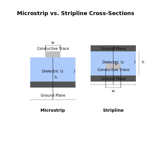
Microstrip and stripline are planar transmission line structures widely used in high-frequency circuit design due to their compatibility with printed circuit board (PCB) fabrication. Microstrip consists of a conductive trace separated from a ground plane by a dielectric substrate, while stripline embeds the trace between two ground planes. The choice between these structures depends on factors such as frequency, impedance control, and crosstalk requirements.
Characteristic Impedance of Microstrip
The characteristic impedance Z0 of a microstrip line depends on the trace width w, substrate height h, and relative permittivity εr. For narrow traces (w/h ≤ 1), the impedance is given by:
where the effective permittivity εeff accounts for the inhomogeneous dielectric environment:
For wider traces (w/h > 1), the impedance is better approximated by:
Stripline Impedance and Propagation
Stripline, being a symmetric structure, offers better shielding and lower radiation losses compared to microstrip. Its characteristic impedance is derived from:
where b is the spacing between ground planes and we is the effective trace width, accounting for fringing fields:
Dispersion and Higher-Order Effects
At frequencies above a few GHz, microstrip exhibits dispersion due to the non-TEM nature of its propagation. The frequency-dependent effective permittivity is modeled by:
where fp is the cutoff frequency for the first higher-order mode:
Practical Design Considerations
- Impedance Matching: Tapered transitions are necessary when connecting microstrip to stripline to minimize reflections.
- Loss Mechanisms: Conductor losses dominate at lower frequencies, while dielectric losses become significant above 10 GHz.
- Manufacturing Tolerances: Etching undercut and substrate thickness variations can cause impedance deviations of ±5%.
Advanced Modeling Techniques
Full-wave electromagnetic simulators (e.g., HFSS, CST) are essential for accurate modeling of:
- Frequency-dependent losses
- Coupling between adjacent traces
- Discontinuities (bends, vias, and T-junctions)
The partial element equivalent circuit (PEEC) method provides a compromise between accuracy and computational efficiency for complex interconnect structures.
5.3 EMI/EMC Considerations
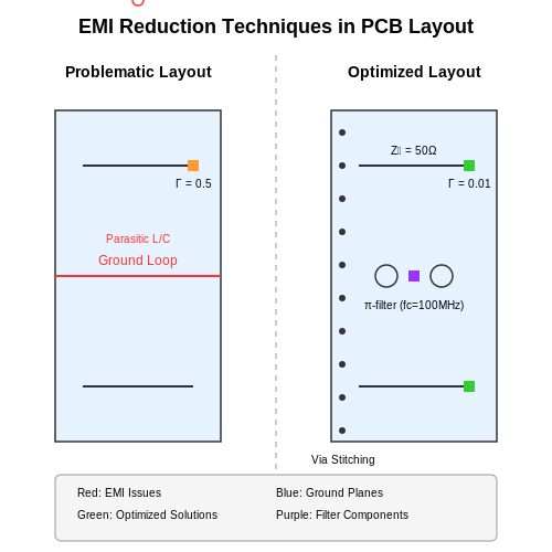
Electromagnetic interference (EMI) and electromagnetic compatibility (EMC) are critical challenges in high-frequency circuit design. Uncontrolled emissions or susceptibility to external noise can degrade performance, violate regulatory standards, or cause system failures. Mitigation requires a systematic approach combining circuit topology, layout techniques, and shielding.
Sources of EMI in High-Frequency Circuits
High-frequency circuits generate EMI through several mechanisms:
- Switching noise from fast digital edges (e.g., clock signals, PWM drivers) produces broadband spectral content.
- Parasitic inductance and capacitance in PCB traces and component leads form unintentional resonant structures.
- Ground loops create differential-mode noise due to impedance mismatches.
- Radiated coupling occurs when trace lengths approach a significant fraction of the signal wavelength.
EMI Reduction Techniques
1. Proper Grounding Strategies
A low-impedance ground plane minimizes voltage gradients and loop areas. For mixed-signal systems, partitioned ground planes with controlled connection points prevent digital noise from coupling into analog sections. The ground impedance Zgnd at frequency f can be approximated as:
where Rdc is the DC resistance and Lparasitic is the inductance of the return path.
2. Transmission Line Termination
Unterminated transmission lines reflect energy, causing ringing and radiation. For a trace with characteristic impedance Z0, the reflection coefficient Γ at a mismatched load ZL is:
Series or parallel termination resistors matching Z0 reduce reflections by minimizing Γ.
3. Shielding and Filtering
Conductive enclosures attenuate radiated emissions via skin effect. The shielding effectiveness (SE) in decibels for a material with thickness t and skin depth δ is:
Ferrite beads and π-filters suppress conducted noise. A second-order LC filter's insertion loss follows:
where fc is the cutoff frequency.
EMC Compliance Testing
Regulatory standards (e.g., FCC Part 15, CISPR 32) define emission limits across frequency bands. Key tests include:
- Radiated emissions measured via antenna in anechoic chambers.
- Conducted emissions evaluated using line impedance stabilization networks (LISNs).
- Immunity testing via RF injection or bulk current injection (BCI).
Pre-compliance testing with near-field probes and spectrum analyzers identifies hotspots early in the design cycle.
Case Study: Reducing Clock Harmonic Radiation
A 2.4 GHz oscillator exhibited excessive emissions at 4.8 GHz (second harmonic). Analysis revealed:
- Inadequate ground stitching vias under the oscillator.
- Unfiltered power supply traces acting as radiating antennas.
Mitigation involved:
- Adding a ground pour with via fencing around the oscillator.
- Implementing a low-pass π-filter on the power rail.
- Using a spread-spectrum clock generator to reduce peak emissions.
Post-optimization measurements showed a 12 dB reduction in harmonic amplitude.
6. SPICE and EM Simulation Tools
6.1 SPICE and EM Simulation Tools
High-frequency circuit design demands precise simulation tools to account for parasitic effects, transmission line behavior, and electromagnetic (EM) coupling. SPICE-based simulators and full-wave EM solvers form the backbone of modern RF and microwave design workflows.
SPICE Simulation for High-Frequency Circuits
SPICE (Simulation Program with Integrated Circuit Emphasis) remains a fundamental tool for analyzing linear and nonlinear circuit behavior. At high frequencies, however, traditional lumped-element approximations break down, necessitating careful modeling of distributed effects. The modified nodal analysis (MNA) approach in SPICE solves Kirchhoff's current and voltage laws in matrix form:
where G is the conductance matrix, x the unknown node voltages and branch currents, and b the source vector. For high-frequency accuracy, SPICE models must incorporate:
- S-parameter blocks for distributed components
- Transmission line models (TXLIN, TLEP)
- Frequency-dependent loss mechanisms (skin effect, dielectric loss)
Electromagnetic Simulation Techniques
Full-wave EM solvers numerically solve Maxwell's equations to capture wave propagation, radiation, and coupling effects. The finite-element method (FEM) discretizes the structure into tetrahedral elements, solving the vector Helmholtz equation:
where E is the electric field, μr relative permeability, εr relative permittivity, and k0 the free-space wavenumber. Key EM solver types include:
- Method of Moments (MoM) for planar structures
- Finite-Difference Time-Domain (FDTD) for broadband analysis
- Finite Element Method (FEM) for arbitrary 3D geometries
Co-Simulation Workflows
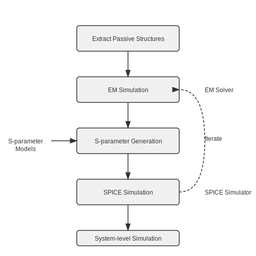
Modern design flows integrate SPICE and EM simulations through hierarchical approaches. A typical workflow:
- Extract critical passive structures (filters, matching networks)
- Simulate in EM solver to generate S-parameter models
- Import S-parameters into SPICE for system-level simulation
- Iterate between EM and circuit simulations
For example, a 28 GHz phased-array element might combine:
- EM simulation of patch antenna and feed network
- SPICE analysis of active phase shifter circuits
- Co-simulation of EM fields and nonlinear device behavior
Practical Considerations
Simulation accuracy depends critically on:
- Mesh density - Must resolve smallest wavelength (λmin/10 rule)
- Material properties - Frequency-dependent εr, tanδ
- Port definitions - Proper waveport vs lumped port selection
- Convergence criteria - Adaptive meshing thresholds
Advanced techniques like parameterized EM models and neural network surrogates accelerate design optimization while maintaining accuracy.
6.2 Vector Network Analyzer (VNA) Measurements
Fundamentals of S-Parameter Measurements
A Vector Network Analyzer (VNA) measures the scattering parameters (S-parameters) of high-frequency networks, providing a complete characterization of linear electrical networks. S-parameters relate incident and reflected waves at each port of a multi-port network:Calibration Techniques for Accurate Measurements
VNA measurements require precise calibration to remove systematic errors introduced by cables, connectors, and fixtures. Common calibration methods include:- Short-Open-Load-Thru (SOLT): Compensates for directivity, source match, and reflection tracking errors.
- Thru-Reflect-Line (TRL): Preferred for non-coaxial environments (e.g., on-wafer measurements).
- Line-Reflect-Match (LRM): Simplified TRL variant for planar structures.
Time-Domain Gating and De-Embedding
Time-domain gating isolates specific reflections by applying an inverse Fourier transform to the frequency-domain data, followed by a windowing function. The gated response is transformed back to the frequency domain, removing unwanted parasitic effects. De-embedding techniques mathematically remove fixture contributions using known standards or electromagnetic simulations. For a fixture with known S-parameters SF, the DUT response is extracted as:Advanced Measurement Considerations
Nonlinear Device Characterization: Modern VNAs support large-signal network analysis (LSNA) by measuring harmonic distortion components. Phase Stability: Temperature-controlled cables and mechanical stabilization reduce phase drift in ultra-precise applications. Mixed-Mode S-Parameters: For differential circuits, mixed-mode S-parameters (Sdd, Sdc, Scd, Scc) are derived from single-ended measurements via transformation matrices.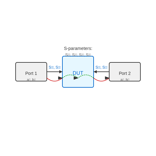
6.3 Time-Domain Reflectometry (TDR)
Fundamentals of TDR
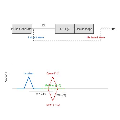
Time-Domain Reflectometry (TDR) is a measurement technique used to characterize impedance discontinuities in transmission lines by analyzing reflected waveforms. A fast-rising step or pulse is injected into the transmission line under test, and the reflected signal is captured. The time delay and amplitude of reflections reveal the location and nature of impedance mismatches.
The reflection coefficient (Γ) at any point along the line is given by:
where ZL is the load impedance and Z0 is the characteristic impedance of the transmission line. A matched load (ZL = Z0) results in Γ = 0, while open (ZL = ∞) and short (ZL = 0) conditions produce reflections of Γ = +1 and Γ = −1, respectively.
TDR Measurement System
A typical TDR setup consists of:
- Pulse Generator: Produces a fast-edge step (rise times < 100 ps for high-resolution analysis).
- Sampling Oscilloscope: Captures incident and reflected waveforms with high temporal resolution.
- Probe Interface: Ensures minimal parasitic loading on the device under test (DUT).
The time delay (Δt) between the incident and reflected pulses determines the distance (d) to the discontinuity:
where vp is the propagation velocity of the signal in the transmission line. For a dielectric with relative permittivity εr, vp = c / \sqrt{εr}, where c is the speed of light.
Applications in High-Frequency Design
TDR is indispensable for:
- Fault Localization: Identifying breaks, shorts, or impedance mismatches in PCBs and cables.
- Interconnect Characterization: Measuring Z0, attenuation, and dispersion in high-speed digital links.
- Package & Connector Analysis: Quantifying parasitic inductances and capacitances in IC packages.
Practical Considerations
Key challenges in TDR measurements include:
- Bandwidth Limitations: The system's rise time limits spatial resolution (Δd ≈ vp ⋅ trise/2).
- Calibration: Requires precise reference standards (e.g., open/short/load) to de-embed probe effects.
- Modal Dispersion: Multiconductor systems (e.g., differential pairs) necessitate mixed-mode TDR analysis.
Advanced TDR Techniques
For multilayer or complex interconnects, Differential TDR and Network Analyzer-Based TDR (using inverse Fourier transforms of frequency-domain data) provide enhanced accuracy. Time-domain simulations in tools like SPICE or ANSYS HFSS can complement empirical TDR data for iterative design refinement.
7. Recommended Textbooks
7.1 Recommended Textbooks
- PDF High-Frequency Integrated Circuits - api.pageplace.de — 4 High-frequency devices 142 4.1 High-frequency active devices 142 4.2 The nanoscale MOSFET 164 4.3 The heterojunction bipolar transistor 219 4.4 The high electron mobility transistor 254 4.5 High-frequency passive components 274 Summary 311 Problems 312 References 314 5 Circuit analysis techniques for high-frequency integrated circuits 318 5.1 Analog versus high-frequency circuit design 318
- High-Frequency Circuit Design and Measurements — High-Frequency Circuit Design and Measurements ... Readers with no prior knowledge in high-frequency circuits are recom mended to read the book in the order that it is arranged. ~ _____ In_t_ro_d_u_c_tl_·o_n _____ ~1 ~ 1 1 Introduction -- 1.1 Trends in electronic circuits and systems -- 1.2 High-frequency circuits -- 1.3 Examples of high ...
- PDF High-Frequency Integrated Circuits - Cambridge University Press ... — 5 Circuit analysis techniques for high-frequency integrated circuits 318 5.1 Analog versus high-frequency circuit design 318 5.2 Impedance matching 321 5.3 Tuned circuit topologies and analysis techniques 335 5.4 Techniques to maximize bandwidth 342 5.5 Challenges in differential circuits at high frequency 356 5.6 Non-linear techniques 362 ...
- PDF Fundamentals of High-Frequency CMOS Analog Integrated Circuits — 3.8 Gain enhancement techniques for high-frequency amplifiers 143 3.8.1 "Additive" approach: distributed amplifiers 144 3.8.2 Cascading strategies for basic gain stages 146 3.8.3 An example: the "Cherry-Hooper" amplifier 148 4 Frequency-selective RF circuits 155 4.1 Resonance circuits 156 4.1.1 The parallel resonance circuit 156
- Electronic Circuit Design Ideas - 1st Edition - Elsevier Shop — Electronic Circuit Design Ideas covers a wide variety of electronic circuit design, which consists of a circuit diagram, waveforms, and an explanation of how the circuit works. ... 7.1 Monolithic Phase-Locked Loop 7.2 Monolithic Tone Decoder 7.3 Dual-Tone Decoder 7.4 Go/No-Go Frequency Meter 7.5 High-Speed, Narrow-Band Tone Decoder 7.6 One ...
- Handbook of Analog Circuit Design - 1st Edition - Elsevier Shop — Frequency-Related Impedance Transformations 7.1 Active Device Behavior above Bandwidth 7.2 Derivation of Bipolar-Junction Transistor High-Frequency Model 7.3 Impedance Transformations in the High-Frequency Region 7.4 Reactance Chart Representation of ß-Gyrated Circuits 7.5 Reactance Chart Stability Criteria for Resonances 7.6 Emitter-Follower ...
- PDF Fast Techniques for Integrated Circuit Design — 978-1-108-49845-6 — Fast Techniques for Integrated Circuit Design Mikael Sahrling Frontmatter ... be it circuit analysis, high frequency phenomena, sampling concepts or jitter, to name a few. The scope of the book is from ... practicing electronics engineers reduce the need for simulators, and help them focus on ...
- Fundamentals of High Frequency CMOS Analog Integrated Circuits — This textbook is ideal for senior undergraduate and graduate courses in RF CMOS circuits, RF circuit design, and high-frequency analog circuit design. It is aimed at electronics engineering students and IC design engineers in the field, wishing to gain a deeper understanding of circuit fundamentals, and to go beyond the widely-used automated ...
- PDF Fundamentals of Electronic Circuit Design - University of Cambridge — 3.8 Simplification Techniques for Determining the Transfer Function 3.8.1 Superposition 3.8.2 Dominant Impedance Approximation 3.8.3 Redrawing Circuits in Different Frequency Ranges 4 Source and Load 4.1 Practical Voltage and Current Sources 4.2 Thevenin and Norton Equivalent Circuits 4.3 Source and Load Model of Electronic Circuits
- High Frequency Circuit Design: with Keysight and MATLAB Design Examples ... — This textbook treats the High Frequency Circuit Design from a practical hands-on approach. Almost all subject matters in the book are accompanied by design examples. University students and practicing engineers will find this book both as a potent learning tool and as a reference guide. The...
7.2 Key Research Papers
- PDF Analog dithering techniques for highly linear and efficient transmitters — 7.1.1 Circuit design 108 7.1.2 Measurement and validation 111 7.2 Self-oscillating class-D 115 7.2.1 Topology design 116 7.2.2 Circuit design 118 7.2.3 Measurement and validation 120 7.2.4 Generic design procedure 122 7.3 Conclusion 123 8.Low frequency dithering 125 8.1 Open loop VMCD 126 8.1.1 Fine tuning of the dithering frequency 128
- PDF High-Frequency Integrated Circuits - api.pageplace.de — 4 High-frequency devices 142 4.1 High-frequency active devices 142 4.2 The nanoscale MOSFET 164 4.3 The heterojunction bipolar transistor 219 4.4 The high electron mobility transistor 254 4.5 High-frequency passive components 274 Summary 311 Problems 312 References 314 5 Circuit analysis techniques for high-frequency integrated circuits 318 5.1 Analog versus high-frequency circuit design 318
- PDF High-Frequency Integrated Circuits - Cambridge University Press ... — 5 Circuit analysis techniques for high-frequency integrated circuits 318 5.1 Analog versus high-frequency circuit design 318 5.2 Impedance matching 321 5.3 Tuned circuit topologies and analysis techniques 335 5.4 Techniques to maximize bandwidth 342 5.5 Challenges in differential circuits at high frequency 356 5.6 Non-linear techniques 362 ...
- Power Management Techniques for Integrated Circuit Design — 5.2 Analysis of Switching Frequency Variation to Reduce Electromagnetic Interference 297 5.2.1 Improvement of Noise Immunity of Feedback Signal 298 5.2.2 Bypassing Path to Filter the High-Frequency Noise of the Feedback Signal 299 5.2.3 Technique of PLL Modulator 302 5.2.4 Full Analysis of Frequency Variation under Different v IN,v OUT, and i ...
- PDF Circuit and Interconnect Design for RF and High Bit-Rate Applications — the gm/id design methodology for cmos analog low power integrated circuits jespers, paul g.a. isbn-10: -387-47100-6 circuit and interconnect design for rf and high bit-rate applications veenstra, hugo, long, john r. isbn: 978-1-4020-6882-9 high-resolution if-to-baseband sigmadelta adc for car radios silva, paulo g.r., huijsing, johan h.
- High-Frequency Circuit Design and Measurements — High-Frequency Circuit Design and Measurements ... An elective course in the final-year BEng progamme in electronic engin eering in the City Polytechnic of Hong Kong was generated in response to the growing need of local industry for graduate engineers capable of designing circuits and performing measurements at high frequencies up to a few ...
- PDF Fundamentals of Electronic Circuit Design - University of Cambridge — 3.8 Simplification Techniques for Determining the Transfer Function 3.8.1 Superposition 3.8.2 Dominant Impedance Approximation 3.8.3 Redrawing Circuits in Different Frequency Ranges 4 Source and Load 4.1 Practical Voltage and Current Sources 4.2 Thevenin and Norton Equivalent Circuits 4.3 Source and Load Model of Electronic Circuits
- PDF Fundamentals of High-Frequency CMOS Analog Integrated Circuits — 3.8 Gain enhancement techniques for high-frequency amplifiers 143 3.8.1 "Additive" approach: distributed amplifiers 144 3.8.2 Cascading strategies for basic gain stages 146 3.8.3 An example: the "Cherry-Hooper" amplifier 148 4 Frequency-selective RF circuits 155 4.1 Resonance circuits 156 4.1.1 The parallel resonance circuit 156
- Radio‐Frequency Integrated‐Circuit Engineering - ResearchGate — Moreover, radio frequency transistors are demonstrated with an extrinsic high cut-off frequency of 7.2 GHz and record high extrinsic maximum frequency of oscillation of 23 GHz, together with ...
- PDF MIT Open Access Articles - Massachusetts Institute of Technology — fixed frequency control techniques to achieve these goals. This paper introduces a quasi-resonant SEPIC converter, resonant gate drive and associated control methods suitable for converter designs at frequencies above 10 MHz. Unlike many resonant converter designs [1]-[4], the proposed approach provides high efficiency over very wide input ...
7.3 Online Resources and Tools
- PDF High-Frequency Integrated Circuits — High-Frequency Integrated Circuits A transistor-level, design-intensive overview of high-speed and high-frequency monolithic integrated circuits for wireless and broadband systems from 2GHz to 200GHz, this comprehensive text covers high-speed, RF, mm-wave, and optical fiber circuits using nanoscale CMOS, SiGe BiCMOS, and III-V technologies. Step-by-step design methodologies, end-of-chapter ...
- High Frequency Communication Electronic Circuit - 中国大学MOOC(慕课) — Course Introduction I. Course Nature and Teaching Purpose High Frequency Communication Electronic Circuit is the main basic course for communication engineering, electronic information engineering, radio wave propagation and electronic science and technology majors. The purpose of this course is to master the basic concept, working principle and circuit composition of each unit circuit of high ...
- RF Circuit Design: Theory and Applications » Outline — Outline Chapter 1: Introduction 1.1 Importance of Radio Frequency Design 1.2 Dimensions and Units 1.3 Frequency Spectrum 1.4 RF Behavior of Passive Components 1.4.1 Resistors at High Frequency 1.4.2 Capacitors at High Frequency 1.4.3 Inductors at High Frequency 1.5 Chip Components and Circuit Board Considerations 1.5.1 Chip Resistors 1.5.2 Chip ...
- High-Frequency Integrated Circuits: Sorin Voinigescu | PDF | Electronic ... — This document provides an overview of high-frequency integrated circuits. It discusses their use in wireless, fiber optic, and imaging systems. It then covers key topics such as modulation techniques, receiver and transmitter architectures, noise analysis, high-frequency devices, circuit analysis techniques, tuned power amplifier design, low-noise amplifier design, mixers, voltage controlled ...
- (BJT) Electronic Circuits Handbook For Design and Application ... - Scribd — The document then discusses the design of integrated high-frequency amplifiers, including using differential amplifiers and common-collector circuits. It covers impedance matching techniques for the input and output, such as terminating resistors or common-base circuits, and how external matching networks are needed at very high frequencies.
- Layout Techniques for Integrated Circuit Designers — The book describes today's manufacturing techniques and how they impact design rules. You will understand how to build common high frequency devices such as inductors, capacitors and T-coils, and will also learn strategies for dealing with high-speed routing both on package level and on-chip applications.
- High-Frequency Circuit Design and Measurements — 1 online resource (226 pages) An elective course in the final-year BEng progamme in electronic engin eering in the City Polytechnic of Hong Kong was generated in response to the growing need of local industry for graduate engineers capable of designing circuits and performing measurements at high frequencies up to a few gigahertz. This book has grown out from the lecture and tutorial ...
- PDF 7 x 11.5 long title.p65 - Cambridge University Press & Assessment — Fundamentals of High-Frequency CMOS Analog Integrated Circuits With a design-centric approach, this textbook bridges the gap between fundamental analog electronic circuits textbooks and more advanced RF IC design texts. The structure and operation of the building blocks of high-frequency ICs are introduced in a systematic manner, with an emphasis on transistor-level operation, the influence of ...
- HIGH FREQUENCY TECHNIQUES - Wiley Online Library — However, in modern engineering, rarely is a classical circuit design used in its standard form, although that was necessar-ily the practice before the availability of personal computers and simulation software.
- PDF AN 958: Board Design Guidelines - Intel — To filter high-frequency noise at the device, place decoupling capacitors as close as possible to each VCC and ground pair. Placing the power and ground planes in parallel and separated by dielectric material provides another level of bypass capacitance.