Tuned RF Amplifiers
1. Definition and Purpose of Tuned RF Amplifiers
Definition and Purpose of Tuned RF Amplifiers
Tuned RF amplifiers are specialized circuits designed to amplify signals within a specific frequency range while rejecting out-of-band interference. They achieve this through resonant LC (inductor-capacitor) networks or other frequency-selective components, enabling high gain and selectivity at radio frequencies (RF). These amplifiers are critical in applications like wireless communication, radar systems, and radio receivers, where precise frequency discrimination is essential.
Core Operating Principle
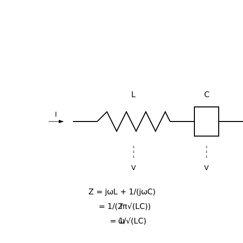
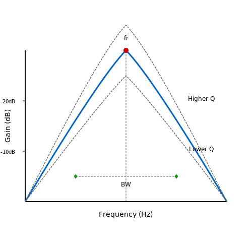
The amplification process in a tuned RF amplifier hinges on the resonance phenomenon. A parallel LC tank circuit, often placed in the collector or drain path of a transistor, acts as a bandpass filter. At resonance, the impedance of the LC network peaks, allowing maximum voltage gain for the desired frequency. The quality factor (Q) of the tank circuit determines the bandwidth (BW) and selectivity:
where fr is the resonant frequency:
Key Characteristics
- Frequency Selectivity: Achieved via tuning elements (e.g., variable capacitors or inductors) to adjust fr dynamically.
- High Gain at Resonance: The amplifier’s gain peaks sharply around fr, attenuating off-resonance signals.
- Stability Considerations: Neutralization techniques may be required to prevent self-oscillation due to parasitic feedback.
Practical Applications
Tuned RF amplifiers are ubiquitous in:
- Superheterodyne Receivers: Selecting and amplifying the intermediate frequency (IF) signal.
- Transmitter Chains: Filtering harmonics and amplifying the carrier wave.
- Spectrum Analysis: Isolating narrowband signals for measurement.
Design Trade-offs
Increasing Q improves selectivity but reduces bandwidth, complicating designs for wideband systems. Stagger-tuning multiple stages can mitigate this, where each stage is tuned to a slightly offset frequency to flatten the passband response.
1.2 Key Characteristics of Tuned RF Amplifiers
Frequency Selectivity and Bandwidth
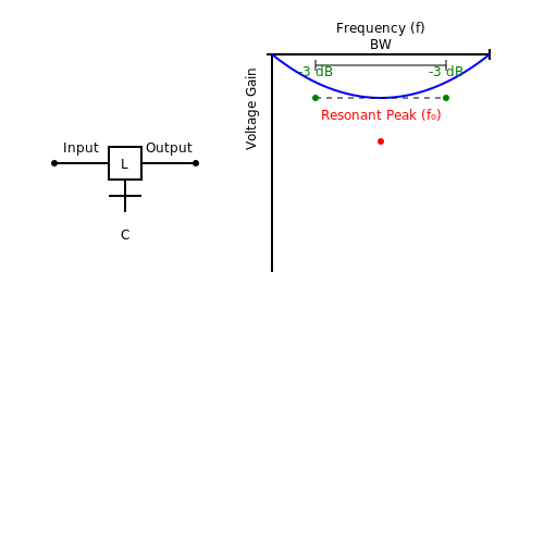
Tuned RF amplifiers derive their frequency selectivity from resonant LC tank circuits. The quality factor Q of the tank circuit determines bandwidth BW according to:
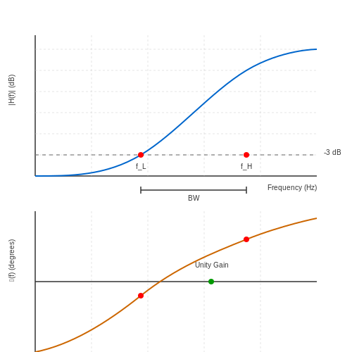
where f0 is the center frequency. High-Q circuits (Q > 100) achieve narrow bandwidths below 1% of f0, critical for channel selection in radio receivers. The -3 dB bandwidth points occur when the reactance equals the resistance in the tank circuit.
Gain and Impedance Matching
Voltage gain in tuned amplifiers peaks at resonance when:
where gm is the transistor transconductance and Ztank is the parallel resonant impedance. Proper impedance matching using tapped inductors or capacitive dividers maximizes power transfer while maintaining selectivity. Mismatching degrades both gain and noise figure.
Stability Considerations
Tuned amplifiers risk instability due to:
- Parasitic feedback through base-collector capacitance (Cμ)
- Insufficient reverse isolation in active devices
- Load impedance variations
The Stern stability factor K must satisfy:
where Δ = S11S22 - S12S21. Neutralization techniques or unilateralization may be required at VHF frequencies and above.
Noise Performance
The noise figure NF of a tuned stage follows:
where Rn is the equivalent noise resistance, and Γ terms represent reflection coefficients. Input matching networks must balance noise matching with power matching constraints.
Nonlinearity and Dynamic Range
Critical nonlinearity metrics include:
- 1-dB compression point (P1dB): Typically 10-20 dB below saturation
- Third-order intercept (IP3): Governed by Taylor series coefficients of transconductance
The dynamic range DR relates to noise floor and compression:
where kTB is the thermal noise power. Cascaded stages require careful gain distribution to maintain system linearity.
Temperature and Process Variation Effects
Key sensitivity factors include:
- Inductor Q degradation with temperature (ΔQ/Q ≈ 0.1%/°C for air-core)
- Capacitor value drift (NP0/C0G dielectrics preferred)
- Transistor fT variation over process corners
Automatic frequency control (AFC) loops or varactor tuning may compensate for drift in critical applications.
1.3 Applications in Modern Electronics
Wireless Communication Systems
Tuned RF amplifiers are fundamental in wireless transceivers, where they selectively amplify narrowband signals while rejecting adjacent channel interference. In 5G NR (New Radio) systems, they enable carrier aggregation by amplifying multiple component carriers simultaneously. The amplifier's quality factor Q directly impacts the signal-to-noise ratio (SNR) in millimeter-wave phased arrays.
where f0 is the center frequency and Δf the bandwidth. Modern implementations use GaN HEMTs with Q > 200 at 28 GHz.
Radar and Sensing Systems
Pulsed Doppler radars employ stagger-tuned amplifiers to handle variable PRF (Pulse Repetition Frequency) while maintaining phase coherence. Automotive 77 GHz radars use SiGe BiCMOS tuned amplifiers with 30 dB gain and < 3 dB noise figure. The cascode topology is preferred for its stability under impedance variations from moving targets.
Medical Imaging
MRI preamplifiers are critically tuned to the Larmor frequency (e.g., 64 MHz for 1.5T systems). Superconducting RF coils achieve unloaded Q factors exceeding 104 by cryogenically cooling the tuned LC tank circuits. This reduces the Johnson-Nyquist noise:
Quantum Computing
Superconducting qubit readout chains use Josephson parametric amplifiers (JPAs) with noise temperatures approaching the quantum limit (Tn ≈ ħω/2kB). These amplifiers are tuned to the qubit transition frequency (4-8 GHz) with bandwidths < 50 MHz to prevent decoherence.
Satellite Communications
Traveling-wave tube amplifiers (TWTAs) in GEO satellites incorporate tunable cavities to compensate for Doppler shifts up to ±50 kHz at Ku-band. Modern solid-state power amplifiers (SSPAs) use adaptive tuning networks with varactor diodes to maintain > 55% efficiency across 500 MHz bandwidths.
Spectrum Analysis
YIG-tuned oscillators in spectrum analyzers provide continuous tuning from 2-40 GHz with phase noise < -110 dBc/Hz at 10 kHz offset. The tuning linearity is maintained through magnetic bias compensation:
where γ is the gyromagnetic ratio (2.8 MHz/Oe).
2. Resonant Circuits in Tuned Amplifiers
Resonant Circuits in Tuned Amplifiers
Fundamentals of Resonance
Resonant circuits form the backbone of tuned RF amplifiers, enabling frequency-selective amplification. A parallel LC circuit exhibits resonance when the inductive and capacitive reactances cancel each other, resulting in a purely resistive impedance at the resonant frequency fr. The quality factor Q determines the bandwidth and selectivity of the circuit.
Impedance Characteristics
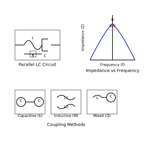
The impedance of a parallel resonant circuit reaches its maximum at resonance and decreases rapidly on either side of fr. This behavior creates the bandpass characteristic essential for tuned amplifiers. The impedance Z at any frequency f can be expressed as:
where R represents the equivalent parallel resistance of the tank circuit. The 3-dB bandwidth BW relates directly to the Q-factor:
Loaded vs Unloaded Q
In practical amplifier designs, we must distinguish between:
- Unloaded Q (Qu): The intrinsic Q of the passive LC components
- Loaded Q (QL): The effective Q when the circuit is coupled to source and load impedances
The loaded Q becomes particularly important when designing multistage amplifiers, as it determines the overall frequency response. The relationship between loaded and unloaded Q is:
where Qext accounts for external loading effects.
Coupling Methods
Three primary techniques exist for coupling resonant circuits in tuned amplifiers:
- Capacitive coupling: Uses series capacitors, providing DC blocking but affecting frequency response
- Inductive coupling: Employs transformer action through mutual inductance
- Mixed coupling: Combines both capacitive and inductive elements for optimized performance
The coupling coefficient k in inductively coupled circuits significantly impacts bandwidth and selectivity:
where M represents the mutual inductance between coils L1 and L2.
Practical Design Considerations
In RF amplifier implementations, several non-ideal factors must be addressed:
- Component losses (particularly in inductors at high frequencies)
- Parasitic capacitances and lead inductances
- Temperature stability of resonant components
- Phase noise considerations in oscillator applications
The effective parallel resistance Rp of an inductor with series resistance Rs transforms at resonance according to:
This transformation highlights why high-Q inductors are critical for maintaining adequate impedance levels in tuned circuits.
2.2 Active Components: Transistors and Tubes
Transistors in RF Amplification
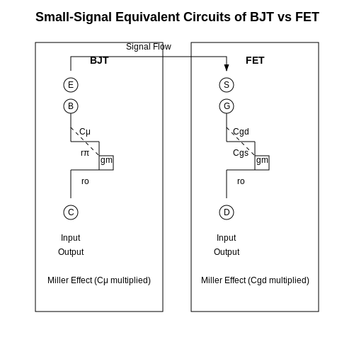
Bipolar Junction Transistors (BJTs) and Field-Effect Transistors (FETs) dominate modern RF amplifier designs due to their high-frequency performance, gain, and efficiency. The small-signal equivalent circuit of a BJT in the common-emitter configuration includes base-emitter resistance rπ, transconductance gm, and output resistance ro. For FETs, the gate-source capacitance Cgs and transconductance gm are critical.
At RF frequencies, parasitic capacitances and inductances become significant. The Miller effect multiplies Cμ (BJTs) or Cgd (FETs), reducing bandwidth. Neutralization techniques or cascode topologies mitigate this.
Vacuum Tubes: Historical and Niche Applications
Despite being largely supplanted by transistors, vacuum tubes like triodes, tetrodes, and klystrons persist in high-power RF systems (e.g., radar, broadcasting). Their advantages include:
- High voltage tolerance – Tubes handle kilovolt-level signals without breakdown.
- Linear operation – Saturation effects are less abrupt than in transistors.
- Thermal robustness – Less prone to thermal runaway.
The transconductance gm of a triode is derived from the Child-Langmuir law:
Comparative Analysis
Transistors excel in size, power efficiency, and integration, while tubes dominate in high-power linearity. The table below summarizes key metrics:
| Parameter | BJTs | FETs | Tubes |
|---|---|---|---|
| Max Frequency | ~100 GHz (SiGe) | ~400 GHz (GaAs) | ~10 GHz |
| Power Handling | ~100 W | ~1 kW (GaN) | >1 MW |
| Linearity (OIP3) | Moderate | High (HEMTs) | Excellent |
Practical Design Considerations
Impedance matching networks (e.g., L-section, π-network) are critical for maximizing power transfer. For BJTs, the optimal load impedance RL is:
Thermal management is paramount, especially for GaN FETs, where junction temperatures above 150°C degrade reliability. Heat sinks and thermal vias are standard solutions.
Passive Components: Inductors and Capacitors
Fundamental Properties
Inductors and capacitors are energy storage elements in RF circuits, exhibiting frequency-dependent behavior critical for tuning and filtering. An inductor stores energy in its magnetic field, with its impedance increasing linearly with frequency:
where L is inductance in henries (H) and ω is angular frequency. Conversely, a capacitor stores energy in its electric field, with impedance decreasing inversely with frequency:
At resonance, the reactances cancel (XL = XC), enabling selective amplification. The quality factor Q quantifies energy storage efficiency:
Parasitic Effects
Real-world components exhibit non-ideal characteristics that dominate at RF frequencies:
- Inductor parasitics: Interwinding capacitance (modeled as parallel C), skin effect increasing AC resistance, and core losses
Equivalent series inductance (ESL) from leads, dielectric absorption, and leakage resistance
The self-resonant frequency (SRF) marks where parasitic capacitance cancels inductive reactance:
Material Considerations
Component materials critically impact performance:
| Component | Material | Key Property |
|---|---|---|
| Inductor | Ferrite | High μr (50-15,000) |
| Capacitor | NP0/C0G | ±30ppm/°C stability |
Practical Implementation
In RF amplifiers, component selection follows these guidelines:
- Use air-core inductors above 50MHz to minimize core losses
- Select capacitors with SRF > 3× operating frequency
- Implement distributed elements (transmission lines) above 1GHz
The impedance transformation ratio for matching networks depends on component Q:
where Q = √(R2/R1 - 1) for L-networks. Multistage matching improves bandwidth when single-stage Q exceeds 10.
Thermal Considerations
Power dissipation in passive components affects stability:
For inductors, core loss dominates at high flux densities:
where α ≈ 1.3-1.6 and β ≈ 2.4-2.8 for MnZn ferrites. Proper heatsinking maintains component parameters within 5% of nominal values.
3. Understanding Frequency Selectivity
3.1 Understanding Frequency Selectivity
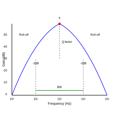
Frequency selectivity in tuned RF amplifiers refers to the ability of a circuit to amplify signals within a specific frequency band while attenuating those outside it. This characteristic is governed by the quality factor (Q) of the resonant circuit, which determines the sharpness of the frequency response.
Quality Factor (Q) and Bandwidth
The quality factor Q is defined as the ratio of the center frequency f₀ to the bandwidth BW of the amplifier:
For a parallel RLC tank circuit, Q can also be expressed in terms of the circuit components:
where R is the equivalent parallel resistance, L is the inductance, and C is the capacitance. A higher Q results in a narrower bandwidth and greater selectivity.
Selectivity and Impedance Matching
The frequency selectivity of a tuned amplifier is closely tied to impedance matching at the resonant frequency. At resonance, the impedance of the parallel RLC circuit reaches its maximum value:
This maximizes voltage gain while minimizing power loss. The impedance falls off rapidly as the frequency deviates from f₀, leading to attenuation of out-of-band signals.
Practical Considerations
In real-world applications, achieving high selectivity involves trade-offs:
- Insertion Loss: Higher Q components (e.g., high-quality inductors) reduce insertion loss but may increase cost.
- Component Tolerances: Variations in L and C values can shift the resonant frequency, affecting selectivity.
- Temperature Stability: Some materials exhibit temperature-dependent properties, necessitating compensation techniques.
Applications in RF Systems
Frequency-selective amplifiers are critical in:
- Radio Receivers: Selecting a desired station while rejecting adjacent channels.
- Wireless Communication: Isolating specific frequency bands in multi-carrier systems (e.g., OFDM).
- Spectrum Analysis: Enhancing resolution in swept-tuned and FFT-based analyzers.
Mathematical Derivation of Selectivity
The transfer function H(f) of a parallel RLC circuit is given by:
At resonance (f = f₀), the imaginary term cancels out, simplifying to:
The -3 dB bandwidth is determined by solving for the frequencies where the magnitude drops to 1/√2:
This yields the bandwidth:
Thus, the selectivity is inversely proportional to Q, with higher Q circuits exhibiting steeper roll-off characteristics.
3.2 Calculating Bandwidth and Q Factor
Bandwidth in Tuned RF Amplifiers
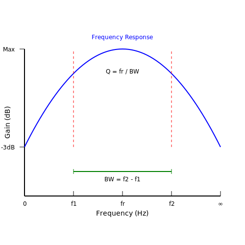
The bandwidth (BW) of a tuned RF amplifier is defined as the frequency range over which the power gain remains within 3 dB of its peak value. For a parallel RLC tank circuit, the bandwidth is determined by the resonant frequency (fr) and the quality factor (Q):
This relationship shows that higher Q results in narrower bandwidth, which is critical for applications requiring high selectivity, such as radio receivers. The 3 dB points (f1 and f2) are calculated as:
Quality Factor (Q) Derivation
The quality factor Q quantifies the energy storage efficiency relative to energy dissipation in the resonant circuit. For a parallel RLC network:
Where:
- R is the equivalent parallel resistance (Ω),
- L is the inductance (H),
- C is the capacitance (F).
For series RLC circuits, the formula inverts:
Practical Implications of Q Factor
High Q circuits (>10) exhibit sharp resonance peaks, making them ideal for filtering specific frequencies. However, they suffer from increased component sensitivity and thermal drift. In contrast, low Q circuits (<5) offer wider bandwidths but reduced gain and selectivity.
Loaded vs. Unloaded Q
The unloaded Q (Qu) represents the intrinsic quality of the passive components, while the loaded Q (QL) accounts for external loading effects (e.g., source/load impedance). The relationship is:
where Qext models external losses. In RF design, impedance matching networks are often used to optimize QL.
Case Study: Superheterodyne Receiver
In a 455 kHz IF stage, a bandwidth of 10 kHz requires:
Achieving this typically involves cascaded double-tuned circuits with staggered resonances to flatten the passband while maintaining edge steepness.
3.3 Impact of Component Tolerances
Frequency Response Deviations
Component tolerances directly affect the resonant frequency (fr) and quality factor (Q) of tuned RF amplifiers. The resonant frequency is given by:
If the inductor (L) or capacitor (C) deviates by ±Δ% from their nominal values, the shift in resonant frequency can be approximated as:
For example, a 5% tolerance in both L and C can lead to a 2.5% shift in fr, potentially misaligning the amplifier’s passband from the desired operating frequency.
Quality Factor Degradation
The quality factor Q depends on component losses, primarily the inductor’s equivalent series resistance (ESR) and capacitor dielectric losses. For a parallel RLC circuit:
Tolerances in R, L, or C alter Q, affecting bandwidth (BW = fr/Q) and selectivity. A 10% increase in ESR can reduce Q by up to 20%, broadening the bandwidth undesirably.
Impedance Mismatch and Power Transfer
Component variations disrupt impedance matching networks, causing reflections. The reflection coefficient (Γ) for a mismatched load ZL is:
Even a 5% deviation in ZL can increase Γ significantly, reducing power transfer efficiency. For instance, a 50Ω system with ZL = 52.5Ω (5% higher) yields:
This corresponds to a return loss of ≈ 32 dB, which may be acceptable, but cascaded mismatches compound the error.
Phase Noise and Stability
Tolerances in reactive components introduce phase shifts, impacting oscillator stability in tuned amplifiers. The phase noise (£(f)) of an LC oscillator is proportional to:
where F is the noise figure, k is Boltzmann’s constant, and Psig is the signal power. A lower Q due to component tolerances elevates phase noise, degrading communication system performance.
Mitigation Strategies
- Use tight-tolerance components (e.g., ±1% capacitors, low-ESR inductors) for critical tuning elements.
- Temperature compensation: Employ NP0/C0G capacitors and stable core materials to minimize drift.
- Active tuning: Implement varactor diodes or digitally tunable capacitors (DTCs) for real-time adjustment.
- Monolithic integration: On-chip LC networks reduce variability but face Q limitations.
In practice, RF designs often use iterative simulation (e.g., Monte Carlo analysis in SPICE) to quantify tolerance effects across production batches.
4. Stability Analysis and Feedback Mechanisms
Stability Analysis and Feedback Mechanisms
Stability Criteria for RF Amplifiers
Stability in tuned RF amplifiers is determined by the absence of unwanted oscillations, which can arise due to parasitic feedback paths. The Rollett stability factor (K) is a critical metric, defined as:
where \( \Delta = S_{11}S_{22} - S_{12}S_{21} \). For unconditional stability, \( K > 1 \) and \( |\Delta| < 1 \) must hold simultaneously. Violations indicate potential instability at certain frequencies or load conditions.
Feedback Mechanisms and Their Impact
Parasitic feedback in RF amplifiers often originates from:
- Internal capacitance (e.g., \( C_{bc} \) in BJTs or \( C_{gd} \) in FETs).
- Layout parasitics (e.g., bond wire inductance or PCB trace coupling).
The open-loop gain \( A \) and feedback factor \( \beta \) determine stability via the Barkhausen criterion:
If this condition is met at any frequency, the amplifier oscillates. Neutralization techniques (e.g., adding cancellation paths) are employed to mitigate this.
Practical Stabilization Techniques
Resistive Loading
Adding a small resistor in series with the base/gate or collector/drain reduces \( Q \)-factor of resonant loops, damping oscillations. The trade-off is reduced gain and efficiency.
Mismatch Loss Intentionality
Deliberately introducing a VSWR mismatch at critical nodes (e.g., \( \Gamma_L \neq S_{22}^* \)) can suppress oscillations. This is quantified by the stability circle analysis on the Smith Chart.
Case Study: Instability in a 2.4 GHz PA
A common pitfall is neglecting package parasitics in power amplifiers. For instance, a 2.4 GHz PA with \( L_{\text{bond}} = 1 \ \text{nH} \) and \( C_{\text{pad}} = 0.5 \ \text{pF} \) forms a resonant tank at:
Though above the operating band, harmonics can excite this resonance, leading to instability. Solutions include:
- Absorptive filters at the output.
- Grounding vias near bond wires to reduce inductance.
Advanced Analysis: Nyquist and Bode Plots
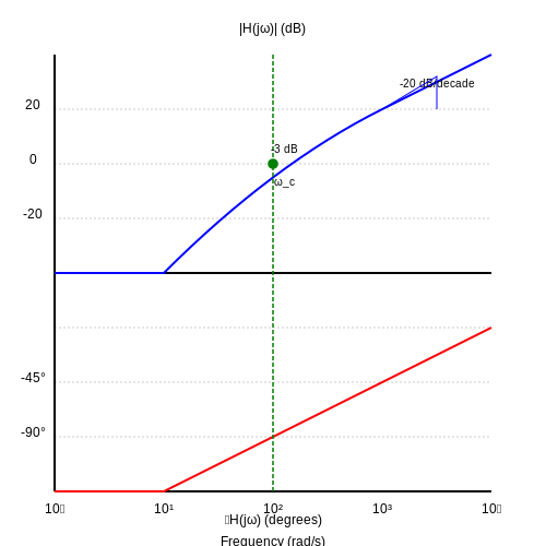
For multi-stage amplifiers, frequency-domain tools like Nyquist plots assess phase margin. A system is stable if the Nyquist curve does not encircle the \( (-1, 0) \) point. Meanwhile, Bode plots of \( |A\beta| \) and \( \angle A\beta \) reveal gain and phase margins:
4.2 Noise Figure and Signal-to-Noise Ratio
Fundamentals of Noise in RF Amplifiers
In RF amplifiers, noise is an unavoidable phenomenon that degrades signal quality. The primary sources of noise include thermal noise (Johnson-Nyquist noise), shot noise, and flicker noise (1/f noise). Thermal noise, generated by random electron motion in resistive components, dominates at high frequencies and is given by:
where k is Boltzmann's constant (1.38 × 10⁻²³ J/K), T is the absolute temperature in Kelvin, and B is the bandwidth in Hz. For a 50 Ω system at room temperature (290 K), the available noise power is −174 dBm/Hz.
Noise Figure Definition
The noise figure (NF) quantifies how much an amplifier degrades the signal-to-noise ratio (SNR) of the input signal. It is defined as:
Expressed in decibels:
An ideal noiseless amplifier would have NF = 0 dB, but practical amplifiers always introduce additional noise. The noise factor F (linear scale) relates to NF via F = 10NF/10.
Cascaded Noise Figure
In multi-stage amplifiers, the total noise figure is governed by Friis' formula:
where Fn and Gn are the noise factor and gain of the n-th stage. This highlights the critical importance of the first stage's noise performance in receiver design.
Signal-to-Noise Ratio (SNR)
SNR measures the ratio of signal power to noise power at a given point in the system:
In logarithmic terms:
For a tuned RF amplifier, the SNR at the output depends on both the input SNR and the amplifier's noise figure:
Minimum Detectable Signal (MDS)
The minimum detectable signal is the weakest input signal that produces a usable output SNR. For a receiver with noise figure NF and bandwidth B, MDS is:
This equation shows how both noise figure and bandwidth directly impact receiver sensitivity.
Noise Temperature
An alternative representation of noise performance is noise temperature (Te), particularly useful in low-noise systems like satellite receivers:
where T0 is the reference temperature (290 K). Noise temperature provides a linear measure of excess noise, making cascade calculations more intuitive in some cases.
Practical Considerations in Tuned RF Amplifiers
In narrowband tuned amplifiers, the noise bandwidth typically equals the -3 dB bandwidth of the tuned circuit. The Q-factor of the tuning network affects both frequency selectivity and noise performance. Higher Q reduces bandwidth but doesn't necessarily improve SNR, as the integrated noise power decreases proportionally with bandwidth.
Modern low-noise amplifiers (LNAs) often employ techniques like:
- Optimal biasing for minimum noise figure
- Impedance matching networks for noise-power match tradeoffs
- Cryogenic cooling in ultra-sensitive applications
- Advanced transistor technologies (HEMT, GaAs) with superior noise performance
The noise figure of a tuned RF amplifier typically ranges from 0.5 dB for cryogenic LNAs to 5 dB or more for room-temperature wideband amplifiers.
4.3 Techniques for Minimizing Distortion
Nonlinearity Compensation via Feedback
Distortion in tuned RF amplifiers primarily arises from nonlinearities in active devices (e.g., BJTs, FETs). Negative feedback reduces harmonic and intermodulation distortion by linearizing the gain characteristic. For a feedback factor β, the closed-loop gain ACL becomes:
where AOL is the open-loop gain. The distortion reduction factor (DRF) scales with loop gain:
Practical implementations use transformer-coupled or capacitive feedback networks to maintain impedance matching while preserving bandwidth.
Predistortion Techniques
Predistortion introduces an inverse nonlinearity before the amplifier to cancel inherent device nonlinearities. For a memoryless system, the output y(t) relates to input x(t) via:
A predistorter applies:
resulting in a linearized composite response. Digital predistortion (DPD) adapts coefficients in real-time using LMS algorithms.
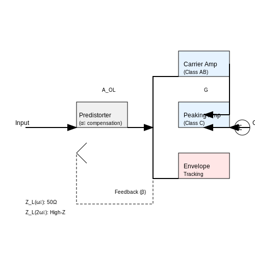
Envelope Tracking and Doherty Architectures
Dynamic supply modulation techniques improve efficiency while reducing AM-AM/AM-PM distortion:
- Envelope Tracking: The supply voltage tracks the RF envelope, keeping the amplifier in compression-free operation.
- Doherty Configuration: A carrier amplifier handles low-power signals while a peaking amplifier activates at high power levels, maintaining linearity across a 6-8 dB backoff range.
Device Biasing Optimization
Class-AB biasing minimizes crossover distortion by maintaining quiescent current IQ:
where θ is the conduction angle. Temperature-compensated bias networks (e.g., VBE multipliers) stabilize the operating point against thermal drift.
Filtering and Load-Pull Matching
Post-amplifier bandpass filters suppress out-of-band harmonics. Load-pull techniques optimize fundamental impedance ZL while presenting high impedances at harmonic frequencies:
Quarter-wave stubs or stepped-impedance networks realize these conditions in microstrip implementations.
Advanced Semiconductor Technologies
GaN HEMTs and LDMOS devices exhibit superior linearity due to:
- Higher breakdown voltages reducing gain compression
- Lower parasitic capacitances minimizing phase distortion
- Improved thermal conductivity preventing parameter shifts
5. PCB Layout and Shielding Techniques
5.1 PCB Layout and Shielding Techniques
Ground Plane Design
A low-impedance ground plane is critical for minimizing parasitic inductance and ensuring stable RF performance. For multilayer PCBs, dedicate at least one full layer as a continuous ground plane. The ground return path for RF currents must be as short as possible to reduce loop inductance, which can degrade amplifier stability and introduce noise. The characteristic impedance of a microstrip trace over a ground plane is given by:
where h is the substrate thickness, w is the trace width, t is the trace thickness, and εr is the dielectric constant. For FR4 material (εr ≈ 4.3), a 50Ω trace typically requires a width-to-height ratio of approximately 2:1.
Component Placement and Routing
Place sensitive RF components (e.g., inductors, capacitors, transistors) first, with minimal trace lengths between them. Avoid right-angle bends in RF traces, as they introduce impedance discontinuities—use curved or 45° mitred bends instead. Critical signal paths should be routed differentially where possible to reject common-mode noise. The crosstalk between adjacent traces follows:
where Cm is the mutual capacitance and Cg is the trace-to-ground capacitance. Maintain a spacing of at least 3× the substrate thickness between parallel RF traces to minimize coupling.
Shielding Techniques
Effective shielding requires a combination of board-level and enclosure-level strategies:
- Faraday Cages: Surround sensitive circuits with grounded copper walls or shielded cans. The shielding effectiveness (SE) in dB is given by:
$$ SE = 20 \log_{10}\left(\frac{E_{unshielded}}{E_{shielded}}\right) $$
- Via Stitching: Place grounded vias at λ/10 intervals along the perimeter of RF sections to suppress cavity resonances. The cutoff frequency for a via fence is:
$$ f_c = \frac{c}{2a\sqrt{\varepsilon_r}} $$where a is the via spacing and c is the speed of light.
- Absorptive Materials: Ferrite tiles or carbon-loaded foam can dampen high-frequency resonances in enclosures.
Power Supply Decoupling
Use a hierarchical decoupling network with capacitors placed in order of decreasing value toward the RF device. The resonant frequency of a decoupling capacitor is:
Place 100nF ceramic capacitors (X7R or C0G dielectric) within 1mm of each power pin, supplemented by bulk 10μF tantalum capacitors. For frequencies above 1GHz, employ distributed capacitance through embedded planar layers.
Thermal Management
RF power devices require careful thermal design to prevent parameter drift. The junction-to-ambient thermal resistance θJA must be minimized through:
- Thermal vias under device pads (array density ≥ 4 vias/mm²)
- Copper pours connected to heatsinks (thermal conductivity of copper: 385 W/m·K)
- Thermal interface materials with conductivity > 5 W/m·K
The temperature rise ΔT is calculated as:
where Pd is the power dissipation. Keep ΔT < 30°C for stable amplifier performance.
5.2 Common Issues and Debugging Methods
Frequency Response Misalignment
Tuned RF amplifiers often suffer from frequency response deviations due to component tolerances or parasitic effects. The loaded quality factor (QL) determines bandwidth, and miscalculations lead to improper tuning. The relationship between QL, center frequency (f0), and bandwidth (BW) is:
Parasitic capacitance (Cp) and inductance (Lp) shift the resonant frequency. Measure using a vector network analyzer (VNA) and compensate by adjusting tank circuit values:
Oscillation and Stability
Unwanted oscillations arise from insufficient isolation between stages or poor grounding. Stability factor (K) must exceed unity for unconditional stability:
where Δ = S11S22 - S12S21. Neutralization techniques or resistive damping may be required if K < 1.
Gain Flatness and Compression
Nonlinearities cause gain compression at high input powers. The 1-dB compression point (P1dB) marks where gain drops by 1 dB from linear behavior. For a tuned amplifier, this is approximated by:
where Vknee is the transistor saturation voltage. Use predistortion or feedback networks to improve linearity.
Thermal Drift
Temperature variations alter component values, shifting resonant frequencies. The thermal coefficient of inductance (TCL) and capacitance (TCC) combine as:
Temperature-compensating capacitors (e.g., NP0/C0G dielectrics) mitigate this effect. Monitor junction temperatures with thermal sensors in critical designs.
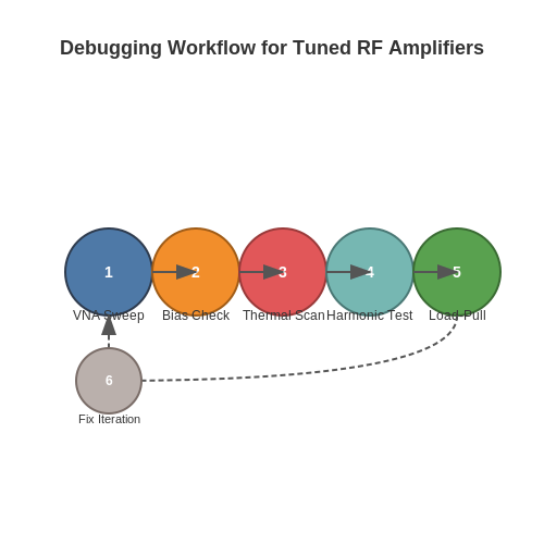
Debugging Workflow
- Spectrum Analysis: Verify spurious emissions and harmonic content using a spectrum analyzer.
- Time-Domain Reflectometry (TDR): Locate impedance mismatches in transmission lines.
- Bias Tee Measurements: Isolate DC bias instability from RF performance issues.
- Load-Pull Analysis: Characterize power transfer under varying load conditions.
5.3 Performance Optimization Strategies
Impedance Matching for Maximum Power Transfer
The efficiency of a tuned RF amplifier heavily depends on impedance matching between stages. Mismatched impedances lead to reflected power, reducing gain and increasing noise. The condition for maximum power transfer is given by:
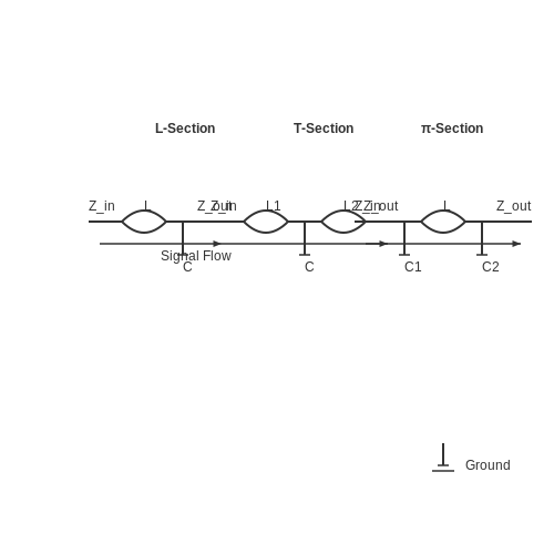
where Zin is the input impedance and Zout is the complex conjugate of the output impedance. Practical implementations often use L-section, T-section, or π-section matching networks to achieve this condition across the desired bandwidth.
Quality Factor (Q) and Bandwidth Trade-offs
The quality factor Q of a tuned circuit determines its selectivity and bandwidth. A higher Q yields sharper frequency response but reduces bandwidth. The relationship is given by:
where BW is the bandwidth and f0 is the resonant frequency. To optimize performance, designers must balance Q to avoid excessive insertion loss while maintaining sufficient selectivity. Stagger-tuning or synchronous tuning techniques can be employed for wider bandwidth applications.
Noise Figure Minimization
In low-noise amplifiers (LNAs), the noise figure (NF) is critical. The Friis formula for cascaded stages highlights the importance of the first amplifier's noise performance:
Strategies to minimize NF include using transistors with low noise parameters (Fmin, Γopt), optimizing bias conditions, and ensuring proper source impedance matching. Cryogenic cooling or advanced semiconductor technologies (e.g., HEMTs) may be employed in ultra-low-noise applications.
Stability Considerations
RF amplifiers must remain unconditionally stable to avoid oscillations. The Rollett stability factor (K) and auxiliary condition (B1) are used to assess stability:
where Δ = S11S22 - S12S21. If K > 1 and B1 > 0, the amplifier is unconditionally stable. Techniques like neutralization or resistive loading can improve stability at the cost of gain.
Linearity and Intermodulation Distortion
High linearity is essential to minimize intermodulation distortion (IMD). The third-order intercept point (IP3) is a key metric:
where ΔP is the difference between fundamental and third-order product power levels. Predistortion techniques, feedback linearization, or back-off from compression can enhance linearity. The choice of active devices (e.g., GaN for high IP3) also plays a significant role.
Thermal Management
Power dissipation affects both performance and reliability. The junction temperature Tj must be controlled to prevent degradation:
where Ta is ambient temperature, Pd is dissipated power, and Rth(j-a) is thermal resistance. Heat sinks, thermal vias, or active cooling systems are common solutions. In high-power applications, load-pull analysis ensures optimal performance under thermal stress.
Advanced Tuning Techniques
Modern amplifiers often employ adaptive tuning to compensate for environmental variations or component aging. Varactor diodes or MEMS-based tunable capacitors enable real-time adjustment of resonant frequencies. Digital predistortion (DPD) algorithms can further optimize performance in software-defined radio (SDR) applications.
6. Recommended Textbooks and Papers
6.1 Recommended Textbooks and Papers
- PDF RF Power Amplifiers for Wireless Communications, 2nd Edition — 1.2 Linear RF Amplifier Theory 2 1.3 Weakly Nonlinear Effects: Power and Volterra Series 5 1.4 Strongly Nonlinear Effects 6 1.5 Nonlinear Device Models for CAD 9 1.6 Conjugate Match 11 1.7 RF Power Device Technology 14 References 15 CHAPTER 2 Linear Power Amplifier Design 17 2.1 Class A Amplifiers and Linear Amplifiers 17 2.2 Gain Match and ...
- PDF RF Microelectronics - pearsoncmg.com — ISBN 978--13-713473-1 (hardcover : alk. paper) 1. Radio frequency integrated circuits—Design and construction. I. Title. TK6560.R39 2011 621.384'12—dc23 2011026820 ... CHAPTER 5 LOW-NOISE AMPLIFIERS 255 5.1 General Considerations 255 5.2 Problem of Input Matching 263 ... 8.5.1 Tuning Range Limitations 521 8.5.2 Effect of Varactor Q 522
- PDF High-Frequency Integrated Circuits - Cambridge University Press ... — 6 Tuned power amplifier design 374 What is a tuned power amplifier? 374 6.1 Tuned PA fundamentals 375 6.2 Classes of tuned PAs and the associated voltage waveforms 377 6.3 Linear modulation of PAs 400 6.4 Class A PA design methodology 401 6.5 Non-idealities in PAs 406 6.6 Implementation examples of CMOS and SiGe HBT mm-wave PAs 407
- Modeling and Design Techniques for Rf Power Amplifiers — Modeling and design techniques for RF power amplifiers i by Arvind Raghavan, Nuttapong Srirattana. Joy Laskar. Includes bibliographical references and index. 1. Power amplifiers-Design and construction. 2. Amplifiers. Radio frequency. TK7871.58.P6R34 2007 62 1.384'126~22 2007027547 Printed in the United States of America. p. cm.
- PDF An Introduction to Radio Frequency Engineering — 1.5 Circuit model of a transmit system. 6 1.6 Conventions for effective length. 6 1.7 A dipole antenna used to collect energy from an electromagnetic wave. 7 1.8 Circuit model of receive system. 7 1.9 Reciprocity principle. 8 1.10 Transmit/receive system. 8 1.11 Noise sources. 9 1.12 Typical antenna noise temperatures for a dipole and a variety of
- Fundamentals of RF and Microwave Transistor Amplifiers — Fundamentals of RF and Microwave Transistor Amplifiers / Inder Bahl. p. cm. Includes bibliographical references and index. ISBN 978--470-39166-2 (cloth) 1. Amplifiers, Radio frequency. 2. Microwave amplifiers. 3. Transistor amplifiers. I. Title. TK6565.A55B26 2009 621.3815 35-dc22 2008049895 Printed in the United States of America ...
- 6 RF Amplifier Design - Springer — 88 6 RF Amplifier Design 6.1.1 NMOS Transistor Basic Expressions In this point we present a brief outline of basic expressions and figures that are used to perform simple analysis of the different circuits. As an starting point, Fig. 6.1 shows the symbol and terminal names that will be used throughout this chapter for NMOS and PMOS transistors.
- PDF Radio Frequency Integrated Circuits and Systems — Focusing on the core topics of RF IC and system design, this textbook provides the in-depth ... 6.2 RF tuned amplifiers 208 6.3 Shunt feedback LNAs 216 6.4 Series feedback LNAs 220 ... Radio Frequency Integrated Circuits and Systems Hooman Darabi Frontmatter
- PDF Introduction to RF Power Amplifier Design and Simulation — Introduction to RF Power Ampli˜er Design and Simulation ˜lls a gap in the existing literature by providing step-by-step guidance for the design of radio frequency (RF) power ampli˜ers, from analytical formulation to simulation, implementation, and measurement. Featuring numerous illustrations and examples of real-world engineering applications,
- PDF 6.1 Adjustment of Loading and Excitation - Arrl — Circuit diagrams of an RF amplifier using triodes in push-pull are shown in sec. 5.4.1. In a push-pull RF amplifier, imbalance in the anode circuit or of anode dissipation is usually due to lack of symmetry in the RF circuit. Normally, the tubes are similar enough that such unbalance is not associated with the tube or its characteristics.
6.2 Online Resources and Tutorials
- PDF RF Power Amplifiers for Wireless Communications, 2nd Edition — 1.2 Linear RF Amplifier Theory 2 1.3 Weakly Nonlinear Effects: Power and Volterra Series 5 1.4 Strongly Nonlinear Effects 6 1.5 Nonlinear Device Models for CAD 9 1.6 Conjugate Match 11 1.7 RF Power Device Technology 14 References 15 CHAPTER 2 Linear Power Amplifier Design 17 2.1 Class A Amplifiers and Linear Amplifiers 17 2.2 Gain Match and ...
- RF Power Amplifiers - The IET - Institution of Engineering and Technology — 1.1 Ideal Parallel-Tuned Circuit 1.2 Ideal Series-Tuned Circuit 1.3 Efficiency 1.4 Collector Efficiency 1.5 Overall Efficiency 1.6 Power-Added Efficiency 1.7 Power Output Capability 1.8 References 2 Classic RF Power Amplifiers 2.1 Class A Amplifiers 2.2 Class B and AB Amplifiers 2.3 Class C Amplifiers 2.4 Bias Circuits
- PDF RF Microelectronics - pearsoncmg.com — 8.5.1 Tuning Range Limitations 521 8.5.2 Effect of Varactor Q 522 8.6 LC VCOs with Wide Tuning Range 524 8.6.1 VCOs with Continuous Tuning 524 8.6.2 Amplitude Variation with Frequency Tuning 532 8.6.3 Discrete Tuning 532 8.7 Phase Noise 536 8.7.1 Basic Concepts 536 8.7.2 Effect of Phase Noise 539 8.7.3 Analysis of Phase Noise: Approach I 544
- High efficiency RF and microwave solid state power amplifiers ... — 1 online resource (xiv, 498 p.) : ill. Series Wiley series in microwave and optical engineering. ... 2.4 The Tuned Load Amplifier. 2.5 Sample Design of a Tuned Load PA. 2.6 References. 3 Nonlinear Analysis for Power Amplifiers. ... "High Efficiency RF and Microwave Solid State Power Amplifiers" is: an ideal tutorial for MSc and postgraduate ...
- PDF High-Frequency Integrated Circuits - Cambridge University Press ... — 6 Tuned power amplifier design 374 What is a tuned power amplifier? 374 6.1 Tuned PA fundamentals 375 6.2 Classes of tuned PAs and the associated voltage waveforms 377 6.3 Linear modulation of PAs 400 6.4 Class A PA design methodology 401 6.5 Non-idealities in PAs 406 6.6 Implementation examples of CMOS and SiGe HBT mm-wave PAs 407
- RF Circuit Design: Theory and Applications » Outline — 8.3 Amplifier Classes of Operation and Biasing Networks 8.3.1 Classes of Operation and Efficiency of Amplifiers 8.3.2 Bipolar Transistor Biasing Networks 8.3.3 Field Effect Transistor Biasing Networks 8.4 Summary Chapter 9: RF Transistor Amplifier Design 9.1 Characteristics of Amplifiers 9.2 Amplifier Power Relations 9.2.1 RF Source
- Linear RF Power Amplifier Design Theory and Principles Online Course — An introduction to load pull analysis in power amplifier design. Chapter 5: Class A Power Amplifier Design. Detailed examples and considerations for designing Class A power amplifiers. Designing load networks in ADS for Class A amplifiers. Chapter 6: Power Amplifier Classes and Efficiency. Understanding the different classes of linear RF power ...
- Applied Electromagnetics/7e by Ulaby and Ravaioli — 2.9 Single-Stub Tuning Tutorial 2.9 Single-Stub Tuning Design 2.10 Transient Response. Chapter 3: Vector Analysis. 3.1 Vector Addition and Subtraction 3.2 Gradient 3.3 Divergence 3.4 Curl. Chapter 4: Electrostatics. 4.1 Fields due to Charges 4.2 Charges in Adjacent Dielectrics 4.3 Charges above a Conducting Plane
- PDF 6.1 Adjustment of Loading and Excitation - Arrl — Circuit diagrams of an RF amplifier using triodes in push-pull are shown in sec. 5.4.1. In a push-pull RF amplifier, imbalance in the anode circuit or of anode dissipation is usually due to lack of symmetry in the RF circuit. Normally, the tubes are similar enough that such unbalance is not associated with the tube or its characteristics.
- PDF Lendi Institute of Engineering and Technology — 1. two stage rc coupled amplifier. 2. rc phase shift oscillator using transistors. 3. class a power amplifier.(series fed) 4. class b complementary symmetry amplifier. 5. current shunt feedback amplifier. 6. single tuned voltage amplifier. 7.hartely oscillator 8.voltage series feed back ampliier 9.class -a transormer coupled power ampifier
6.3 Advanced Topics for Further Study
- Advanced Design Techniques for RF Power Amplifiers (Analog Circuits and ... — Advanced Design Techniques for RF Power Amplifiers' main aim is to provide the reader with a deep analysis of theoretical aspects, modelling, and design strategies of RF high-efficiency power amplifiers. Advanced Design Techniques for RF Power Amplifiers begins with an analytical review of current state of the problem.
- PDF EXTRA TOPICS RELATED TO x6 Filters and Tuned Amplifiers — l shape of the frequency response of a tuned amplifier. The techniques discussed apply to amplifiers with center frequencies in the rang of a few hundred kilohertz to a few hundred megahertz. Tuned amplifiers find application in the radio-frequency (RF) and intermediate-frequency (IF) sections of com
- High efficiency RF and microwave solid state power amplifiers ... — "High Efficiency RF and Microwave Solid State Power Amplifiers" is: an ideal tutorial for MSc and postgraduate students taking courses in microwave electronics and solid state circuit/device design; and, a useful reference text for practicing electronic engineers and researchers in the field of PA design and microwave and RF engineering.
- PDF 6 Small-signal Amplifiers: Advanced Topics - Springer — 6 Small-signal Amplifiers: Advanced Topics Coverage Examination of some advanced circuit techniques: bootstrapping to increase input resistance, efficient biasing using current mirrors and the use of an active load to obtain very high voltage gain.
- PDF Advanced Techniques in RF Power Amplifier Design (Ripped by sabbanji) — This is not really an advanced book, but does cover topics which are generally of a less elemen-tary, or tutorial, nature than my first book. In RF Power Amplifiers for Wire-less Communications (RFPA, also published by Artech House), my overriding goal was to present the subject material in a manner that is analytical but hopefully still readable.
- CST Microwave Studio Advanced Topics Manual - Forum for Electronics — See section 4.7 of the CST MWS Advanced Topics Manual (attached below) for a discussion of the use of Auto-Regressive (AR) Filtering. Sorry to upload the whole manual, but I could not separate the section of interest...
- PDF A Study and Comparison of Efficiency Enhancement Techniques for RF ... — A Study and Comparison of Efficiency Enhancement Techniques for RF Power Amplifiers Geoffrey N. Mendenhall, P.E. VP Transmission Research and Technology Harris Broadcast Communications, Mason, Ohio
- PDF Microsoft Word - Chapter 6_Part.docx - Concordia University — The reason is that with small values (and hence small sizes) of L, C elements, the resonant frequency o 1/ LC can be very high i.e., 100 KHz - 100 MHz. Further the tuned load circuit does not consume any DC power. The response of a tuned amplifier resembles a band-pass characteristic.
- PDF An Introduction to Radio Frequency Engineering — An Introduction to Radio Frequency Engineering This book provides a comprehensive introduction to radio frequency (RF) engineering, using a straightforward and easily understood approach combined with numerous worked examples, illustrations and homework problems. The author has focused on minimising the mathematics needed to grasp the subject while providing a solid theoretical foundation for ...
- PDF Radio Frequency Integrated Circuits and Systems — Frequency Systems Focusing on the core topics of RF IC and system design, this textbook provides the in-depth coverage and detailed mathematical analyses needed to gain a thorough understanding of the subject. Throughout, theory is linked to practice with real-world application examples; practical design guidance is also offered, covering the pros and cons of various topologies, and preparing ...