Piezoelectric Sensors and Actuators
1. Definition and Basic Principles
Piezoelectric Sensors and Actuators: Definition and Basic Principles
Fundamental Piezoelectric Effect
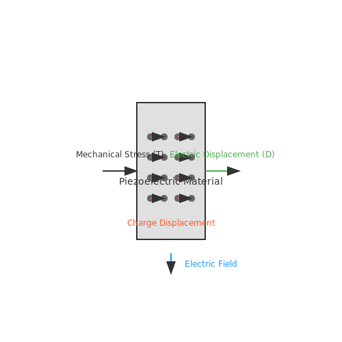
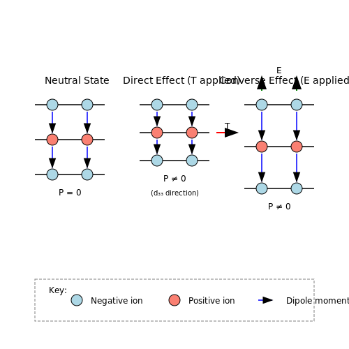
The piezoelectric effect is a linear electromechanical interaction between mechanical and electrical states in crystalline materials without inversion symmetry. This phenomenon manifests in two forms:
- Direct piezoelectric effect: Generation of electric charge in response to applied mechanical stress
- Converse piezoelectric effect: Mechanical deformation in response to applied electric field
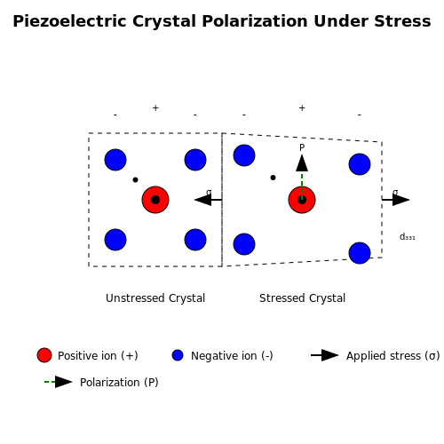
The effect arises from the displacement of ionic charges within the crystal lattice when subjected to stress, creating a net dipole moment. For a crystal with 3m symmetry, the piezoelectric constitutive equations are:
where D is electric displacement, T is stress, E is electric field, S is strain, d is piezoelectric coefficient, ε is permittivity, and s is elastic compliance.
Crystal Structures and Materials
Common piezoelectric materials fall into three categories:
- Single crystals: Quartz (SiO2), Lithium Niobate (LiNbO3)
- Ceramics: Lead Zirconate Titanate (PZT), Barium Titanate (BaTiO3)
- Polymers: Polyvinylidene Fluoride (PVDF)
The crystal structure determines the piezoelectric coefficients. For example, in PZT ceramics, the perovskite structure (ABO3) allows for large d33 coefficients (typically 200-600 pC/N) through poling of ferroelectric domains.
Piezoelectric Coupling Coefficient
The electromechanical coupling factor k represents energy conversion efficiency:
For a thin piezoelectric disk in thickness vibration mode, the coupling coefficient is:
Practical values range from 0.1 for PVDF to 0.7 for high-performance PZT compositions.
Sensor and Actuator Configurations
Piezoelectric transducers operate in various modes:
| Mode | Configuration | Typical Application |
|---|---|---|
| Thickness expansion (d33) | Electric field parallel to polarization | High-force actuators |
| Transverse expansion (d31) | Electric field perpendicular to polarization | Bending actuators |
| Shear mode (d15) | Electric field perpendicular to polarization and strain | Ultrasonic transducers |
Practical Considerations
Key performance parameters include:
- Curie temperature: Maximum operating temperature before depolarization
- Mechanical quality factor (Qm): Ratio of stored to dissipated energy
- Impedance matching: Critical for energy transfer in ultrasonic applications
The frequency response of a piezoelectric element is governed by its resonant behavior, with fundamental resonance occurring at:
where t is thickness, c33D is elastic stiffness at constant electric displacement, and ρ is density.
1.2 Piezoelectric Materials and Their Properties
Crystal Structure and Polarization Mechanisms
The piezoelectric effect arises from non-centrosymmetric crystal structures, where mechanical stress disrupts charge symmetry, generating a dipole moment. Materials like quartz (SiO2) exhibit this due to their trigonal crystal system, while perovskites like lead zirconate titanate (PZT) rely on oxygen octahedron tilting. The polarization P is given by:
where dijk is the piezoelectric coefficient tensor, σjk the applied stress, and Ej the electric field. For poled ceramics, the d33 coefficient (axial mode) dominates, often exceeding 300 pC/N in PZT-5H.
Key Material Classes
- Single Crystals (e.g., Quartz, LiNbO3): High stability and low losses (Q > 105), but limited coupling coefficients (kt ~ 0.1).
- Polycrystalline Ceramics (e.g., PZT, BaTiO3): Tunable via doping (e.g., La3+ for "soft" PZT with high d33).
- Polymers (e.g., PVDF): Flexible with d31 ~ 20 pC/N, but low Curie temperatures (~80°C).
Performance Metrics
The electromechanical coupling factor k quantifies energy conversion efficiency:
For PZT-5A, k33 ≈ 0.7, while PVDF achieves only ≈0.1. Frequency constants (e.g., 2000 Hz·m for PZT-8) govern resonant behavior in ultrasonic transducers.
Thermal and Environmental Stability
Curie temperature (TC) defines the upper operational limit (e.g., 350°C for PZT-4 vs. 120°C for PVDF). Aging in ceramics follows a logarithmic decay law due to domain wall pinning:
where m is the aging rate (typically 1–3%/decade for stabilized compositions).
Emerging Materials
Relaxor ferroelectrics like PMN-PT exhibit ultrahigh d33 (>2000 pC/N) but narrow temperature ranges. Textured ceramics (e.g., <001>-oriented PZT) bridge single-crystal and polycrystalline performance.
1.3 Direct and Inverse Piezoelectric Effects
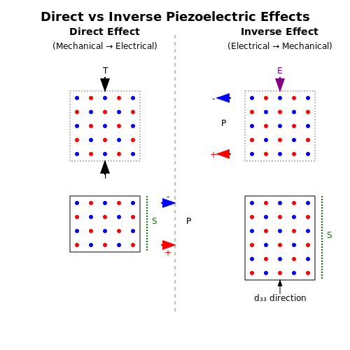
The piezoelectric effect is a fundamental electromechanical coupling phenomenon that manifests in two distinct forms: the direct piezoelectric effect and the inverse piezoelectric effect. These effects are governed by the same underlying physics but differ in their energy conversion direction.
Direct Piezoelectric Effect
The direct piezoelectric effect describes the generation of electric charge in response to applied mechanical stress. When a piezoelectric material is subjected to strain, its crystal lattice deforms, causing a displacement of positive and negative charge centers. This results in a net polarization P proportional to the stress T:
where dijk is the third-rank piezoelectric coefficient tensor (units: C/N or m/V). For a simplified case of uniaxial stress along the poling direction (3-axis), this reduces to:
Common applications exploiting this effect include:
- Pressure sensors in automotive fuel injection systems
- Vibration monitoring in industrial equipment
- Ultrasonic receivers in medical imaging
Inverse Piezoelectric Effect
The inverse effect describes mechanical deformation in response to an applied electric field. An external field E induces lattice strain S through:
For the same poled ceramic under field along the 3-axis, the dominant strain component is:
This effect enables precise motion control in:
- Nanopositioning stages for microscopy
- Fuel injector valves with sub-millisecond response
- Ultrasonic transmitters for sonar systems
Tensor Symmetry Considerations
The piezoelectric coefficient tensor dijk exhibits specific symmetries based on crystal structure. For poled ceramics (∞m symmetry), the matrix representation simplifies to:
where the contracted notation (Voigt form) converts ijk to mn indices. The three independent coefficients d33, d31, and d15 completely describe the material's response.
Energy Conversion Efficiency
The electromechanical coupling factor k quantifies energy conversion efficiency between domains:
For longitudinal mode operation, this relates to material constants through:
where YE is Young's modulus at constant field and ϵT33 is permittivity at constant stress. Typical PZT ceramics achieve k33 values of 0.6-0.7.
2. Working Principle of Piezoelectric Sensors
2.1 Working Principle of Piezoelectric Sensors
The piezoelectric effect is the fundamental mechanism behind piezoelectric sensors, where mechanical stress induces an electric charge in certain crystalline materials. This phenomenon was first discovered by Pierre and Jacques Curie in 1880 and is governed by the direct piezoelectric effect, mathematically expressed as:
where Q is the generated charge, dij is the piezoelectric coefficient tensor (C/N), and F is the applied force. The subscripts i and j denote the direction of the electrical and mechanical axes, respectively, highlighting the anisotropic nature of piezoelectric materials.
Crystallographic Basis of Piezoelectricity
Piezoelectricity arises in non-centrosymmetric crystal structures, such as quartz (SiO2), lead zirconate titanate (PZT), and barium titanate (BaTiO3). When mechanical stress is applied, the unit cell deforms, displacing positive and negative charge centers and creating a dipole moment. The net polarization P across the material is given by:
where pi is the dipole moment of the i-th unit cell and V is the volume. For a sensor with electrode area A and thickness t, the open-circuit voltage Voc generated is:
where gij is the voltage coefficient (Vm/N), σ is the applied stress, and εr is the relative permittivity.
Sensor Configurations and Modes of Operation
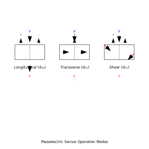
Piezoelectric sensors operate in three primary modes:
- Longitudinal mode (d33): Force applied along the poling direction, producing charge separation parallel to the force.
- Transverse mode (d31): Force applied perpendicular to poling, generating charge in the orthogonal direction.
- Shear mode (d15): Tangential force induces polarization through crystal lattice distortion.
The effective charge sensitivity Sq (pC/N) varies with mode and material properties:
Equivalent Circuit and Frequency Response
The electrical behavior of a piezoelectric sensor is modeled as a charge generator with parallel capacitance Cp and leakage resistance Rp:
This results in a high-pass characteristic with cutoff frequency fc = 1/(2πRpCp). For quasi-static measurements, charge amplifiers with feedback capacitance Cf are employed to mitigate the inherent drift.
Practical Considerations
Key design parameters include:
- Resonant frequency: Dictated by mechanical dimensions and elastic modulus
- Temperature stability: Pyroelectric effects may introduce noise in varying thermal environments
- Impedance matching: High output impedance requires low-noise preamplification
Modern applications leverage these principles in precision force measurement, acoustic emission detection, and dynamic pressure sensing, with advanced materials like PMN-PT single crystals achieving d33 coefficients exceeding 2000 pC/N.
2.2 Common Types of Piezoelectric Sensors
Quartz-Based Piezoelectric Sensors
Quartz (SiO2) is one of the most widely used piezoelectric materials due to its high stability, low temperature coefficient, and excellent mechanical quality factor (Q). The piezoelectric effect in quartz arises from its crystalline structure, where applied mechanical stress generates an electric dipole moment. The charge sensitivity d11 for quartz is approximately 2.3 pC/N along the X-axis. Quartz sensors are commonly employed in precision applications such as accelerometers, pressure sensors, and frequency control devices like crystal oscillators.
Lead Zirconate Titanate (PZT) Sensors
PZT ceramics (Pb[ZrxTi1-x]O3) exhibit significantly higher piezoelectric coefficients (d33 ≈ 300-600 pC/N) compared to quartz, making them ideal for high-sensitivity applications. The enhanced performance stems from the engineered domain structure achieved through poling. The governing equation for charge generation is:
where Q is the generated charge, d33 is the piezoelectric coefficient, and F is the applied force. PZT sensors dominate in ultrasonic transducers, energy harvesting systems, and vibration monitoring applications due to their high electromechanical coupling coefficient (kt > 0.5).
Polyvinylidene Fluoride (PVDF) Sensors
PVDF is a flexible polymer piezoelectric material with unique advantages for conformal sensing applications. Unlike rigid ceramics, PVDF films can be manufactured in thicknesses as low as 9 μm, enabling high-frequency response (>100 MHz). The piezoelectric activity originates from the alignment of molecular dipoles during poling, described by:
where e31 is the piezoelectric stress constant and c11E is the elastic stiffness at constant electric field. PVDF sensors are extensively used in biomedical applications, touch sensors, and acoustic transducers due to their mechanical flexibility and acoustic impedance matching with water and biological tissues.
Lithium Niobate (LiNbO3) Sensors
Single-crystal lithium niobate offers exceptional temperature stability (up to 1000°C) and high electromechanical coupling (k33 ≈ 0.49). The material's non-centrosymmetric crystal structure (point group 3m) gives rise to strong piezoelectric response along the Z-axis. Surface acoustic wave (SAW) devices utilizing LiNbO3 substrates achieve GHz-range operation for RF filters and chemical sensors, with the wave velocity given by:
where c44 is the shear elastic constant and ρ is the material density.
Barium Titanate (BaTiO3) Sensors
As one of the first discovered piezoelectric ceramics, BaTiO3 remains important for its high permittivity (εr > 1000) near the Curie temperature (120°C). The tetragonal phase below TC exhibits spontaneous polarization that can be aligned through poling. Modern doped variants (e.g., BaTiO3-CaTiO3) achieve improved temperature stability for applications in underwater transducers and piezoelectric transformers.
Comparison of Key Parameters
| Material | d33 (pC/N) | εr | TC (°C) |
|---|---|---|---|
| Quartz | 2.3 (d11) | 4.5 | 573 |
| PZT-5A | 374 | 1700 | 365 |
| PVDF | -33 | 12 | ~100 |
| LiNbO3 | 16 | 30 | 1210 |
The selection of piezoelectric sensor material involves trade-offs between sensitivity, temperature range, mechanical properties, and environmental stability. Recent advances in composite materials (e.g., 1-3 PZT-polymer composites) combine the benefits of multiple material systems for specialized applications.
2.3 Applications in Measurement and Monitoring
Piezoelectric sensors and actuators are widely employed in precision measurement and monitoring systems due to their high sensitivity, fast response, and ability to operate in harsh environments. Their applications span multiple disciplines, including structural health monitoring, biomedical instrumentation, and industrial process control.
Structural Health Monitoring (SHM)
In civil and aerospace engineering, piezoelectric transducers are embedded in structures to detect mechanical stress, strain, and crack propagation. When subjected to dynamic loads, these sensors generate voltage signals proportional to the applied stress. The relationship between strain (ε) and piezoelectric output voltage (V) is given by:
where gij is the piezoelectric voltage coefficient (in V·m/N), σ is the stress, and t is the thickness of the piezoelectric material. Arrays of such sensors enable real-time damage detection through techniques like electromechanical impedance (EMI) analysis.
Biomedical Sensing
Piezoelectric elements are crucial in medical ultrasound imaging, where they convert electrical pulses into mechanical vibrations (actuation) and vice versa (sensing). The center frequency (fc) of a piezoelectric ultrasound transducer is determined by:
where v is the speed of sound in the piezoelectric material and d is its thickness. This principle also applies to implantable pressure sensors, where lead zirconate titanate (PZT) films monitor intracranial or cardiovascular pressure with resolutions below 1 mmHg.
Industrial Process Monitoring
In manufacturing environments, piezoelectric accelerometers measure vibration spectra to predict equipment failure. The charge output (Q) from such sensors under acceleration (a) follows:
where dij is the charge coefficient and m is the seismic mass. Advanced systems integrate these sensors with machine learning algorithms to identify anomalous vibration patterns indicative of bearing wear or imbalance.
Acoustic Emission Detection
Piezoelectric sensors detect high-frequency stress waves (50 kHz–1 MHz) generated by material deformation. The signal-to-noise ratio (SNR) in such applications depends on the piezoelectric material's figure of merit:
where d is the piezoelectric strain coefficient and g is the voltage coefficient. This makes PZT-5H the preferred choice for detecting microcracks in pressure vessels and pipelines.
Energy Harvesting in Sensor Networks
Self-powered monitoring systems utilize piezoelectric energy harvesters that convert ambient vibrations into electrical energy. The maximum power (Pmax) extractable from a resonant piezoelectric harvester is:
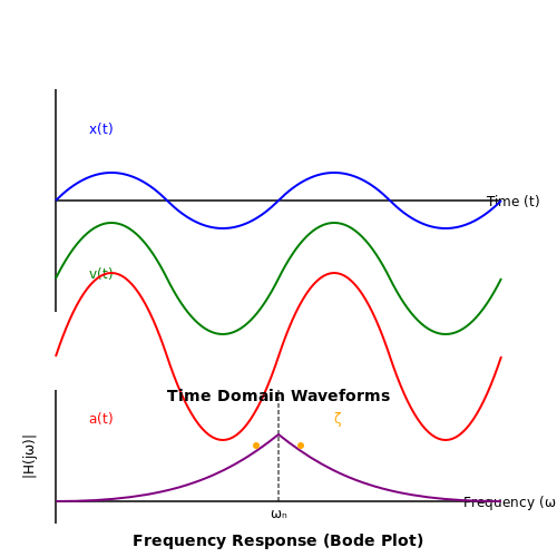
where Y is the base excitation amplitude, ωn is the natural frequency, and ζ is the damping ratio. Such systems enable wireless sensor nodes in remote structural monitoring applications.
3. Working Principle of Piezoelectric Actuators
3.1 Working Principle of Piezoelectric Actuators
Piezoelectric actuators operate based on the inverse piezoelectric effect, where an applied electric field induces mechanical deformation in a piezoelectric material. The relationship between the induced strain (S) and the applied electric field (E) is governed by the piezoelectric charge constant (d):
For a piezoelectric actuator subjected to a voltage V across its thickness t, the resulting displacement ΔL is:
where d33 is the longitudinal piezoelectric coefficient and L is the actuator length. In shear mode (d15), the displacement occurs perpendicular to the applied field.
Electromechanical Coupling
The complete constitutive equations for piezoelectric materials combine Hooke's law with the piezoelectric effect:
where T is stress, cE is elastic stiffness at constant electric field, e is the piezoelectric stress constant, and εS is permittivity at constant strain.
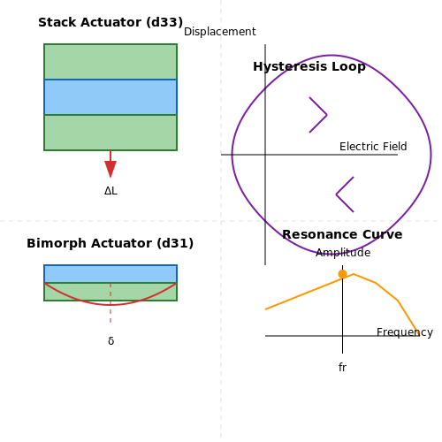
Hysteresis and Nonlinearity
Practical piezoelectric actuators exhibit nonlinear behavior due to:
- Ferroelectric domain wall motion (butterfly hysteresis)
- Creep effects in step responses
- Temperature-dependent coefficients
The Preisach model describes hysteresis through a weighted superposition of elementary relays:
Stack and Bimorph Configurations
Stack actuators employ multiple piezoelectric layers electrically connected in parallel and mechanically in series, providing high force (up to 10 kN) but limited stroke (typically 0.1-0.2% of length). The total displacement scales linearly with layer count N:
Bimorph actuators consist of two bonded piezoelectric layers poled in opposite directions, producing bending motion. The tip deflection δ for a cantilever bimorph is:
Resonance and Dynamic Response
The mechanical resonance frequency fr of a piezoelectric actuator depends on its dimensions and material properties:
where ρ is the material density. Above resonance, the actuator response rolls off at -40 dB/decade due to second-order mechanical dynamics.
3.2 Types of Piezoelectric Actuators
Piezoelectric actuators convert electrical energy into precise mechanical displacement, leveraging the inverse piezoelectric effect. Their performance depends on material properties, structural configuration, and driving mechanisms. Below are the primary types of piezoelectric actuators, each optimized for specific applications.
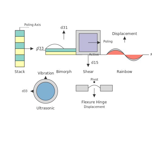
Stack Actuators
Stack actuators consist of multiple thin piezoelectric layers bonded in series, electrically connected in parallel. This configuration maximizes displacement along the poling direction while minimizing driving voltage. The total displacement ΔL of an n-layer stack is given by:
where d33 is the piezoelectric coefficient and V is the applied voltage. These actuators are widely used in nanopositioning systems, adaptive optics, and fuel injection systems due to their high force generation (up to several kN) and sub-nanometer resolution.
Bimorph Actuators
Bimorph actuators comprise two piezoelectric layers bonded together, often with a passive shim. When voltage is applied, one layer expands while the other contracts, producing bending motion. The tip deflection δ of a cantilevered bimorph is:
where L is length, t is thickness, and d31 is the transverse piezoelectric coefficient. Bimorphs excel in low-force, high-displacement applications such as ultrasonic motors and microfluidic pumps.
Shear Actuators
Shear actuators utilize the d15 coefficient, generating in-plane motion perpendicular to the poling direction. The shear strain γ is:
where E is the applied electric field. These actuators are critical in torsional and shear-mode applications, including vibration damping and rotary positioning systems.
Rainbow Actuators
Rainbow actuators employ a reduced chemical gradient to create internal stresses, enhancing displacement via buckling. The displacement amplification factor A is approximated by:
where tactive and treduced are thicknesses of the active and reduced layers. These actuators are used in energy harvesting and large-stroke positioning.
Ultrasonic Piezoelectric Actuators
Ultrasonic actuators operate at resonant frequencies, combining standing waves with frictional coupling to achieve motion. The linear velocity v is governed by:
where f is frequency and A is vibration amplitude. These actuators are prevalent in autofocus mechanisms and precision linear stages.
Amplified Piezoelectric Actuators
Amplified actuators use mechanical leverage (e.g., flexure hinges) to magnify displacement. The amplification ratio R depends on the hinge geometry:
Such designs are essential in aerospace and semiconductor manufacturing, where micron-level accuracy is required over millimeter ranges.
3.3 Applications in Precision Positioning and Control
Piezoelectric actuators are indispensable in precision positioning systems due to their sub-nanometer resolution, high stiffness, and rapid response times. Unlike traditional electromagnetic actuators, piezoelectric devices operate on the inverse piezoelectric effect, where an applied electric field induces mechanical strain, enabling precise motion control without backlash or friction.
Nanopositioning Systems
In atomic force microscopy (AFM) and scanning tunneling microscopy (STM), piezoelectric actuators facilitate sub-Ångström displacements. The actuator's displacement x is governed by:
where dij is the piezoelectric coefficient, E the electric field, and L the actuator length. For lead zirconate titanate (PZT), d33 ≈ 500 pm/V, enabling displacements of 50 nm per 100 V applied across a 10 mm actuator.
Closed-Loop Control with Feedback Sensors
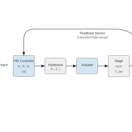
To mitigate hysteresis and creep—key nonlinearities in piezoelectric materials—closed-loop systems integrate capacitive or strain-gauge feedback. The control law for a PID-compensated piezo stage is:
where e(t) is the position error. Modern systems augment this with feedforward hysteresis models like the Preisach or Krasnosel'skii-Pokrovskii operators.
Adaptive Optics and Beam Steering
In adaptive optics, piezoelectric deformable mirrors correct wavefront distortions at kHz rates. The influence function Fi(x,y) of each actuator is approximated by:
where (xi, yi) denotes actuator locations and σ the Gaussian coupling coefficient. Stroke ranges of 15–20 µm with 0.1% linearity are typical for PZT-based mirrors.
Industrial Automation Case Study
In semiconductor lithography, piezoelectric stages achieve ±1 nm repeatability over 200 mm travel. A dual-stage system combines coarse (voice coil) and fine (piezo) actuators, with the latter compensating high-frequency disturbances via:
where m, c, and k are the stage mass, damping, and stiffness, respectively. Such systems enable ≤3 nm overlay errors in EUV lithography.
Emerging Applications
Recent advances include:
- Piezoelectric inchworm motors for long-range nanopositioning (e.g., 20 mm travel at 0.1 nm resolution)
- Resonant piezoelectric actuators in MEMS mirrors for LiDAR, operating at >100 kHz with <1 µrad jitter
- Hybrid flexure designs combining piezoelectric and electrostatic actuation for 6-DOF alignment
4. Material Selection for Piezoelectric Devices
4.1 Material Selection for Piezoelectric Devices
The performance of piezoelectric sensors and actuators is critically dependent on the choice of material, which governs key parameters such as piezoelectric coefficients, electromechanical coupling factors, dielectric permittivity, and mechanical compliance. The selection process must balance these properties against environmental stability, manufacturability, and cost.
Key Material Properties
The effectiveness of a piezoelectric material is quantified by its piezoelectric charge coefficient (dij) and voltage coefficient (gij), which relate mechanical strain to electric polarization and vice versa. The constitutive equations are:
where Di is electric displacement, Tjk is stress, Ej is electric field, Sij is strain, and sijklE is compliance at constant electric field. The superscripts T and E denote conditions of constant stress or electric field, respectively.
Common Piezoelectric Materials
1. Lead Zirconate Titanate (PZT)
PZT ceramics dominate industrial applications due to their high piezoelectric coefficients (d33 ≈ 200–600 pC/N) and Curie temperatures (150–350°C). Their properties can be tuned by varying the Zr/Ti ratio or doping with donors (e.g., Nb5+) or acceptors (e.g., Fe3+).
2. Barium Titanate (BaTiO3)
BaTiO3 was the first discovered perovskite piezoelectric, with a d33 of ~190 pC/N. Its lower Curie temperature (120°C) limits high-temperature use, but it remains popular for biocompatible and lead-free applications.
3. Polyvinylidene Fluoride (PVDF)
PVDF is a flexible polymer with d31 ≈ 20–30 pC/N. Its low acoustic impedance makes it ideal for medical ultrasound, though its temperature stability is inferior to ceramics.
Emerging Materials
Aluminum Nitride (AlN) offers CMOS compatibility and high thermal conductivity, while ZnO is used in thin-film transducers. Single crystals like PMN-PT exhibit exceptional d33 (>2000 pC/N) but are costly and fragile.
Selection Criteria
- Operating Frequency: High-frequency applications (>10 MHz) require low-loss materials like AlN.
- Temperature Range: PZT is preferred for >100°C environments, while PVDF degrades above 80°C.
- Mechanical Load: Hard PZT (e.g., Navy Type III) withstands high stress, whereas soft PZT (Type I) offers higher sensitivity.
Case Study: Energy Harvesting
In vibration energy harvesters, the electromechanical coupling factor (k2) determines efficiency. For a cantilever beam, the optimal material maximizes:
where Y is Young’s modulus. PZT-5H (k2 ≈ 0.5) outperforms PVDF (k2 ≈ 0.1) but requires careful stress management.
4.2 Fabrication Techniques and Challenges
Thin-Film Deposition Methods
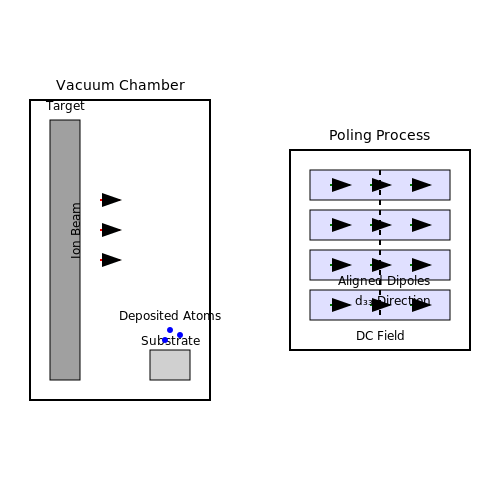
Piezoelectric thin films are commonly fabricated using physical vapor deposition (PVD) and chemical vapor deposition (CVD) techniques. Sputtering, a PVD method, involves bombarding a target material with ions in a vacuum chamber, ejecting atoms that deposit onto a substrate. The sputtering parameters—such as power, pressure, and substrate temperature—critically influence film quality. For example, excessive power can induce defects, while insufficient heating may lead to poor crystallinity. CVD techniques, including metal-organic CVD (MOCVD), enable precise stoichiometric control but require careful management of precursor gases and reaction kinetics.
Bulk Material Processing
For bulk piezoelectric ceramics like PZT (lead zirconate titanate), the conventional process involves solid-state synthesis. Raw powders of PbO, ZrO2, and TiO2 are mixed, calcined at 800–900°C, and sintered at 1200–1300°C. The sintering process must balance densification with lead volatility, which can degrade stoichiometry. Hot pressing or spark plasma sintering (SPS) can achieve higher densities at lower temperatures, mitigating lead loss. Single-crystal growth, such as PMN-PT (lead magnesium niobate-lead titanate), employs the Bridgman method, requiring precise thermal gradients to avoid cracking.
Microelectromechanical Systems (MEMS) Integration
MEMS-based piezoelectric devices demand compatibility with semiconductor fabrication. Challenges include:
- Stress-induced delamination: Mismatched thermal expansion coefficients between piezoelectric films (e.g., AlN) and silicon substrates cause cracking.
- Etch selectivity: Dry etching (e.g., reactive ion etching) must preserve piezoelectric layers while patterning electrodes.
- Pollution control: Lead-containing materials require specialized handling to meet environmental regulations.
Poling and Domain Alignment
The piezoelectric effect requires aligned ferroelectric domains, achieved through poling. A DC electric field (1–3 kV/mm) is applied at elevated temperatures (100–150°C for PZT) to orient dipoles. Incomplete poling reduces the effective piezoelectric coefficient (d33). For thin films, poling is complicated by substrate clamping, which restricts domain reorientation. Recent advances use alternating fields or laser-assisted poling to improve alignment.
Scalability and Yield Challenges
Industrial-scale production faces trade-offs between performance and reproducibility. For instance, sol-gel deposition offers excellent film uniformity but suffers from cracking during pyrolysis. Inkjet printing enables rapid prototyping but struggles with achieving high piezoelectric coefficients. Yield losses often stem from:
- Electrode adhesion: Poor bonding between Pt/Ti electrodes and PZT causes delamination.
- Grain boundary defects: Randomly oriented grains in polycrystalline films reduce coupling efficiency.
- Process variability: Minor fluctuations in annealing temperature (±5°C) can alter crystallographic phase.
Emerging Techniques
Additive manufacturing (3D printing) of piezoelectric polymers like PVDF enables complex geometries but lags in resolution (< 50 µm). Atomic layer deposition (ALD) achieves sub-nanometer thickness control but is prohibitively slow for thick films. Heterogeneous integration with flexible substrates (e.g., polyimide) introduces new challenges in thermal budget management.
4.3 Performance Optimization Strategies
Material Selection and Poling Optimization
The electromechanical coupling coefficient k is a critical parameter for piezoelectric performance, defined as:
where d is the piezoelectric charge constant, sE is the elastic compliance at constant electric field, and ϵT is the permittivity at constant stress. To maximize k:
- Single crystal materials like PMN-PT exhibit k33 > 0.9 but are costly
- Poling field strength should exceed 2 kV/mm for PZT ceramics
- Poling temperature should be near the Curie point (typically 120-150°C for PZT-5H)
Mechanical Preloading Techniques
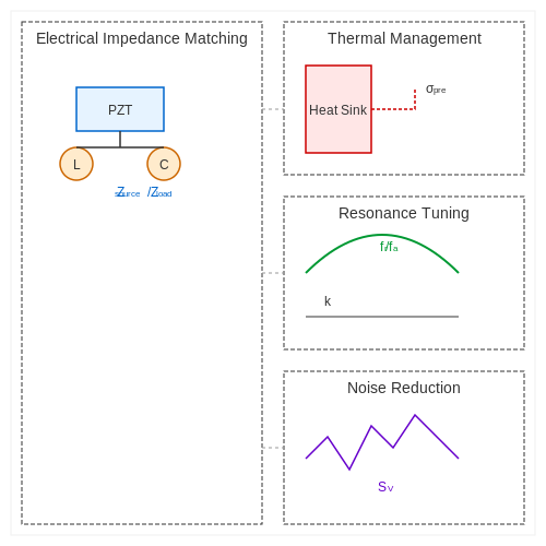
Compressive preloading improves linearity and prevents tensile failure. The optimal preload stress σpre follows:
where σc is the compressive strength (typically 400-600 MPa for PZT). Stack actuators benefit from Belleville washers maintaining 50-100 N/mm2 preload.
Electrical Impedance Matching
Power transfer maximizes when source and load impedances satisfy:
For a typical PZT element with capacitance Cp = 10 nF at 1 kHz, the reactive component dominates (XC ≈ 16 kΩ). Inductive matching networks can cancel this reactance:
Thermal Management
The heat generation rate Q̇ in cyclic operation is:
where tan δ is the loss tangent (0.01-0.03 for PZT). Active cooling maintains temperature below 80°C to prevent depoling. Thermal vias in multilayer designs reduce thermal resistance by 40-60%.
Resonance Tuning
The effective coupling coefficient keff at resonance depends on modal alignment:
where fr and fa are resonant and anti-resonant frequencies. Mass loading adjustments can shift resonance by ±15% while maintaining keff > 0.7.
Noise Reduction Methods
Voltage noise spectral density SV in sensor mode relates to:
where Rp is the leakage resistance (>1 GΩ for quality PZT). Charge amplifiers with Rf > 1 TΩ and Cf < 1 pF achieve noise floors below 1 μV/√Hz.
5. Interface Circuits for Piezoelectric Sensors
5.1 Interface Circuits for Piezoelectric Sensors
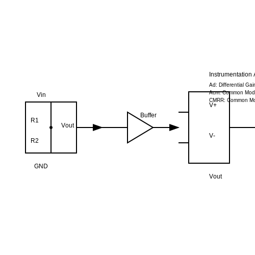
Piezoelectric sensors generate high-impedance charge signals in response to mechanical stress, necessitating specialized interface circuits to condition the output for measurement systems. The two primary approaches are charge amplifiers and voltage amplifiers, each with distinct advantages depending on application requirements.
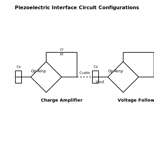
Charge Amplifier Configuration
The charge amplifier converts the sensor's generated charge into a proportional voltage while minimizing signal distortion. Its operation relies on an operational amplifier with capacitive feedback:
where Q is the generated charge and Cf is the feedback capacitance. The circuit's transfer function demonstrates its ability to maintain sensitivity independent of cable capacitance:
where A is the open-loop gain and β is the feedback factor. Practical implementations require:
- Ultra-low bias current op-amps (JFET or CMOS input stages)
- High-quality feedback capacitors with low dielectric absorption
- Parallel feedback resistor (typically 100MΩ-1GΩ) for DC stabilization
Voltage Follower Approach
For high-frequency applications where cable capacitance is negligible, a simple voltage follower may suffice. The output voltage relates directly to the piezoelectric element's inherent capacitance:
This configuration becomes problematic when Ccable approaches or exceeds Cp, causing significant signal attenuation. Modern solutions often incorporate:
- Impedance buffers with ultra-high input impedance (>1013Ω)
- Guard rings to minimize leakage currents
- Low-noise JFET input stages
Noise Considerations
The total noise equivalent charge (NEQ) of a piezoelectric measurement system combines contributions from:
where en is the voltage noise density, in is the current noise density, and Ctotal is the sum of sensor, cable, and amplifier input capacitances. Optimal noise performance requires:
- Minimizing parasitic capacitances in the signal path
- Selecting amplifiers with noise corners below the bandwidth of interest
- Using proper shielding techniques to reduce electromagnetic interference
Advanced Interface Techniques
Recent developments in interface electronics include:
- Digital charge converters with built-in sigma-delta ADCs for direct digital output
- Resonant tracking circuits for energy harvesting applications
- Adaptive bias networks that compensate for pyroelectric effects in multi-domain sensors
For high-channel-count systems, integrated solutions like the Analog Devices AD7768 or Texas Instruments PGA970 provide complete signal chains with programmable gain and filtering.
5.2 Driving Circuits for Piezoelectric Actuators
Piezoelectric actuators require specialized driving circuits to achieve precise control over displacement, force, and response time. The driving circuit must account for the actuator's capacitive nature, high-voltage requirements, and dynamic behavior under varying loads.
Voltage Requirements and Capacitive Load
Piezoelectric actuators typically operate at high voltages (50–1000 V) and present a capacitive load, with capacitance values ranging from nanofarads to microfarads. The required current I to drive the actuator at a given slew rate dV/dt is derived from:
where C is the actuator's capacitance. For a 100 nF actuator driven at 100 V/µs, the current demand is 10 mA. Insufficient current delivery leads to sluggish response, while excessive current can cause overheating.
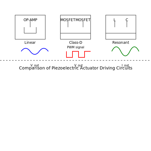
Linear Amplifier Circuits
Linear amplifiers provide low-noise, high-precision driving but suffer from low efficiency due to power dissipation in the output stage. A basic operational amplifier (op-amp) based high-voltage driver uses a push-pull configuration:
The circuit's bandwidth is limited by the op-amp's slew rate and the RC time constant formed by the actuator's capacitance and output impedance.
Switching (Class-D) Amplifiers
For high-efficiency applications, switching amplifiers modulate the output voltage using pulse-width modulation (PWM). A half-bridge or full-bridge topology generates bipolar voltages:
where D is the duty cycle. Switching frequencies typically range from 20 kHz to 1 MHz, with higher frequencies reducing ripple but increasing switching losses.
Resonant Drive Circuits
Resonant circuits minimize power dissipation by matching the driving frequency to the actuator's mechanical resonance. An LC tank circuit stores energy cyclically:
where L is an external inductor tuned to the actuator's capacitance C. This method is particularly effective for ultrasonic actuators operating at fixed frequencies.
Charge Control vs. Voltage Control
Traditional voltage control leads to hysteresis and creep due to the actuator's nonlinear capacitance. Charge control improves linearity by directly regulating the stored charge:
Charge pumps or switched-capacitor circuits implement this approach, though they require precise current monitoring and feedback.
Protection and Decoupling
High-voltage transients and back-EMF necessitate protection diodes and snubber circuits. Decoupling capacitors placed close to the actuator stabilize the supply voltage during rapid current transients.
Practical Considerations
- Grounding: Separate analog and power grounds to minimize noise coupling.
- Feedback: Strain gauges or capacitive sensors provide closed-loop control.
- Thermal Management: High-voltage drivers require heat sinks or active cooling.
5.3 Noise Reduction and Signal Processing Techniques
Sources of Noise in Piezoelectric Systems
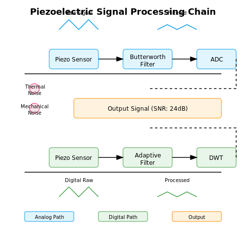
Piezoelectric sensors and actuators are susceptible to various noise sources, including thermal noise, mechanical vibrations, and electromagnetic interference (EMI). Thermal noise arises from Brownian motion of charge carriers and is modeled by the Johnson-Nyquist equation:
where kB is Boltzmann's constant, T is temperature, R is resistance, and Δf is bandwidth. Mechanical vibrations introduce spurious signals that can alias into the measurement bandwidth, while EMI couples capacitively or inductively into high-impedance piezoelectric circuits.
Analog Filtering Techniques
First-stage signal conditioning often employs passive or active analog filters to attenuate out-of-band noise. A Butterworth low-pass filter is commonly used for its maximally flat passband response. The transfer function of a second-order Butterworth filter is:
where ωc is the cutoff frequency. For piezoelectric systems operating in the 1-100 kHz range, Sallen-Key active filters using low-noise op-amps (e.g., AD797) achieve sub-nanovolt noise floors.
Digital Signal Processing Methods
After analog-to-digital conversion, several digital techniques further enhance signal quality:
- Adaptive filtering: LMS algorithms dynamically cancel noise correlated with reference signals
- Wavelet denoising: Thresholding in wavelet domains preserves transient features while removing noise
- Lock-in amplification: Synchronous detection extracts signals buried in 60 dB+ noise
The discrete wavelet transform (DWT) decomposition is particularly effective for non-stationary piezoelectric signals:
where ψ is the mother wavelet, a is the scale parameter, and b is the shift parameter.
Shielding and Grounding Strategies
Proper electromagnetic shielding reduces capacitive coupling of interference. A coaxial cable with driven guard (active shielding) maintains the shield at sensor potential, eliminating leakage currents. For high-impedance piezoelectric systems (>1 MΩ), guard rings on PCBs and triaxial cables provide 40-60 dB noise rejection.
Case Study: Ultrasonic Transducer Array
In a 64-element medical ultrasound array, combining analog filtering (8th-order Chebyshev at 15 MHz) with digital matched filtering improved the signal-to-noise ratio from 12 dB to 28 dB. The matched filter impulse response h[n] was designed as the time-reversed transmit pulse:
where s[n] is the known transmit waveform. This approach achieved 150 μm axial resolution at 5 MHz center frequency.
6. Emerging Applications in Biomedical Engineering
6.1 Emerging Applications in Biomedical Engineering
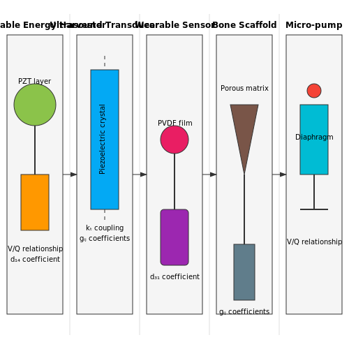
Energy Harvesting for Implantable Devices
Piezoelectric materials are increasingly being utilized to power implantable medical devices by converting biomechanical energy into electrical energy. The human body provides a rich source of mechanical energy from heartbeats, blood flow, and muscle movements. A piezoelectric energy harvester can be modeled using the constitutive equations:
where V is the generated voltage, gij is the piezoelectric voltage coefficient, σj is the applied stress, and t is the material thickness. For PZT-5H, typical values of g33 range from 19.7 to 24.8×10⁻³ Vm/N, making it suitable for low-power applications like pacemakers and neurostimulators.
Ultrasound Transducers for Imaging and Therapy
Piezoelectric transducers form the core of medical ultrasound systems. The transmit-receive response is governed by the electromechanical coupling factor kt:
where e33 is the piezoelectric stress constant, c33D is the elastic stiffness at constant electric displacement, and ϵ33S is the permittivity at constant strain. Modern transducers use PMN-PT single crystals with kt > 0.5, enabling higher resolution imaging and targeted drug delivery through ultrasonic cavitation.
Wearable Health Monitoring Systems
Flexible piezoelectric sensors based on PVDF or P(VDF-TrFE) copolymers are being integrated into wearable patches for continuous vital sign monitoring. The charge output Q from such sensors follows:
where d31 is the transverse piezoelectric coefficient, F is the applied force, and L, w, t are the sensor dimensions. These systems can detect arterial pulse waves with sensitivity exceeding 0.1 kPa-1, enabling continuous blood pressure monitoring without cuffs.
Bone Growth Stimulation
Piezoelectric scaffolds for bone tissue engineering exploit the endogenous piezoelectricity of collagen (≈0.2 pC/N). The applied electric field E generated under mechanical loading enhances osteoblast proliferation through:
where d14 is the shear piezoelectric coefficient, γ is the shear strain, and ϵ is the relative permittivity. Clinical studies show BaTiO3-based scaffolds can accelerate bone regeneration by 40% compared to non-piezoelectric controls.
Precision Drug Delivery
Piezoelectric micro-pumps enable controlled drug release through the relationship between flow rate Q and driving voltage V:
where r is the actuator radius, f is the driving frequency, and t is the diaphragm thickness. Systems using PZT diaphragms achieve dosing precision of ±2% at flow rates down to 0.1 μL/min, critical for chemotherapy and insulin delivery.
6.2 Energy Harvesting Using Piezoelectric Materials
Fundamentals of Piezoelectric Energy Harvesting
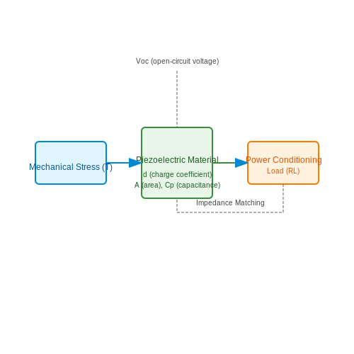
Piezoelectric energy harvesting converts mechanical vibrations or strain into electrical energy via the direct piezoelectric effect. The governing equation for the generated charge Q due to an applied stress T is:
where d is the piezoelectric charge coefficient (C/N) and A is the electrode area. The open-circuit voltage Voc is derived from:
where Cp is the capacitance, εr is the relative permittivity, and t is the material thickness.
Power Output Optimization
The maximum power transfer occurs when the load impedance matches the source impedance (RL = 1/ωCp). The power P harvested from sinusoidal vibrations of frequency ω and displacement y0 is:
where Y is Young’s modulus. For broadband energy harvesting, techniques like frequency up-conversion or multi-resonator arrays are employed.
Practical Considerations
- Material Selection: PZT-5H and PVDF are common, with PZT offering higher power density (~300 μW/cm3) but PVDF providing flexibility.
- Resonant vs. Non-resonant Operation: Resonant systems (e.g., cantilevers) maximize output at specific frequencies, while non-resonant designs (e.g., stacks) suit quasi-static loads.
- Power Conditioning: AC-DC converters with active rectification (e.g., synchronous switches) improve efficiency over passive diode bridges.
Applications
Piezoelectric harvesters power wireless sensor nodes (e.g., structural health monitoring), wearable electronics, and IoT devices. Case studies include:
- Footstep Energy Harvesting: Embedded PZT tiles in walkways generate 1–10 mW per step.
- Industrial Vibration Harvesting: MFC (Macro Fiber Composite) patches on machinery yield 0.5–5 mW/cm2 at 50–200 Hz.
Limitations and Research Frontiers
Challenges include low energy density (~1–10 mW/cm3), impedance mismatch, and fatigue in cyclic loading. Emerging solutions:
- Hybrid Harvesters: Combining piezoelectric with electromagnetic or triboelectric mechanisms.
- Advanced Materials: Single-crystal PMN-PT for higher d33 (>2000 pC/N).
- Adaptive Circuits: Maximum power point tracking (MPPT) algorithms for dynamic loads.
6.3 Innovations in Smart Structures and IoT
Energy Harvesting and Self-Powered Systems
Piezoelectric materials have enabled the development of self-powered IoT nodes by converting ambient mechanical vibrations into usable electrical energy. The power output P of a piezoelectric energy harvester can be derived from the constitutive equations:
where k is the electromechanical coupling coefficient, ω is the angular frequency of vibrations, F is the applied force, and Z is the mechanical impedance. Recent advances in low-power electronics have reduced the operational threshold to sub-milliwatt levels, making piezoelectric harvesters viable for wireless sensor networks.
Structural Health Monitoring
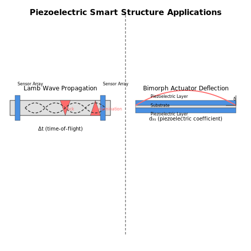
Embedded piezoelectric sensor arrays are revolutionizing structural health monitoring in civil and aerospace applications. By analyzing Lamb wave propagation through materials, defects such as cracks or delaminations can be detected with sub-millimeter resolution. The time-of-flight Δt of an acoustic wave between two piezoelectric transducers is given by:
where d is the distance between transducers, E is Young's modulus, ρ is material density, and ν is Poisson's ratio. Machine learning algorithms now enable real-time damage classification with >95% accuracy in composite materials.
Adaptive Morphing Structures
Piezoelectric actuators are enabling shape-changing aerodynamic surfaces with response times under 10 ms. The maximum deflection δ of a bimorph piezoelectric actuator is:
where d31 is the piezoelectric coefficient, V is applied voltage, L is length, and t is thickness. Boeing's Morphing Aerostructure demonstrator achieved 12° trailing edge deflection using this principle, reducing drag by 8% during flight tests.
Distributed Sensing Networks
Smart skin systems integrate thousands of piezoelectric micro-sensors (<1 mm2 footprint) with edge computing nodes. The signal-to-noise ratio (SNR) for such arrays follows:
where N is the number of elements, d33 is the piezoelectric coefficient, σ is applied stress, kB is Boltzmann's constant, T is temperature, R is resistance, and Δf is bandwidth. DARPA's SHIELD program demonstrated 5000-element arrays with 40 dB SNR at 1 kHz bandwidth.
5G-Enabled Piezoelectric Systems
The ultra-low latency of 5G networks (<1 ms) allows closed-loop control of piezoelectric actuators at kHz rates. The stability criterion for such systems requires:
where τcontrol is the total latency and fres is the mechanical resonance frequency. Nokia Bell Labs recently demonstrated a 5G-connected piezoelectric active noise cancellation system achieving 30 dB attenuation up to 800 Hz.
7. Key Research Papers and Books
7.1 Key Research Papers and Books
- PDF Piezoelectric sensors and actuators : fundamentals and applications - GBV — Contents 1 Introduction 1.1 Fundamentals of Sensors and Actuators 1.2 History of Piezoelectricity and Piezoelectric Materials
- Piezoelectric Sensors and Actuators - springerprofessional.de — This book introduces physical effects and fundamentals of piezoelectric sensors and actuators. It gives a comprehensive overview of piezoelectric materials such as quartz crystals and polycrystalline ceramic materials. Different modeling approaches and methods to precisely predict the behavior of piezoelectric devices are described. Furthermore, a simulation-based approach is detailed which ...
- (PDF) A Systematic Review of Piezoelectric Materials and Energy ... — The piezoelectric materials have shown key characteristics for engineering applications, such as in sensors and actuators for industrial use. Because of their excellent mechanical-to-electrical and vice versa energy conversion properties, piezoelectric materials with high piezoelectric charge and voltage coefficient have been tested in ...
- PDF Integration and Deployment of Thick Film Piezoelectric Actuators ... — Ultrasonic sensing systems typically consist of multiple piezoelectric elements which function as both actuators and sensors. The systems function by using one piezoelectric element to actuate a strain wave into th
- From synthesis to application: High-quality flexible piezoelectric ... — Her research aims at the synthesis and characterization of piezoelectric materials, piezo-mechatronic devices, energy harvesting, MEMS/NEMS, flexible electronic, sensors and actuators.
- (PDF) Piezoelectricity and Its Applications - ResearchGate — In addition, this article discusses the latest techniques for utilizing the piezoelectric materials in energy harvesters, sensors and actuators for various building systems.
- Simulation of Piezoelectric Sensor and Actuator Devices — Nowadays, computer simulations play a key role in the design, optimization, and characterization of piezoelectric sensor and actuator devices. The primary reason for this lies in the fact that simulations as an important step in computer-aided engineering (CAE) allow to predict the device behavior without fabricating expensive prototypes.
- Piezoelectric Materials: Properties, Advancements, and Design ... — The piezoelectric effect is that, upon an external load being posed on an object, electrical potential generates on its surface. Piezoelectric materials can serve as crucial units for energy-harvesting equipment or as active parts of sensors, and so on [2].
- Coupled field analysis of piezoelectric materials for sensor and ... — Piezoelectric materials are found in a variety of everyday gadgets, including automotive electronic devices, mobile phone parts, surface acoustic wave devices, and so on. Within various sensor modules are piezoelectric materials that accomplish the desired function.
- PDF thesis.dvi - Purdue University — The aim of this work is to study the behavior of a piezoelectric actuator in order to get a better understanding of various important dynamic phenomena associated with the actuator. The results of this work are to help in further research in pre-cisely modelling piezoelectric actuators either for simulation and open-loop feedfor-ward compensation or closed-loop feedback control when these ...
7.2 Online Resources and Tutorials
- Piezoelectric Sensors and Actuators | springerprofessional.de — Piezoelectric sensors and actuators make a substantial contribution in this respect. At the beginning of the opening chapter, we will discuss the fundamentals of sensors and actuators. Section 1.2 addresses the history of piezoelectricity and piezoelectric materials. ... Electronic ISBN 978-3-662-57534-5. Print ISBN 978-3-662-57532-1. DOI https ...
- PDF Piezoelectric sensors and actuators : fundamentals and applications - GBV — 2.1 Electromagnetics 7 2.1.1 Maxwell'sEquations 7 2.1.2 Electrostatic Field 9 2.1.3 Interface Conditions for Electric Field 10 2.1.4 LumpedCircuit Elements 12 2.2 Continuum Mechanics 15 ... Piezoelectric sensors and actuators : fundamentals and applications Subject: Berlin, Springer, 2019 Keywords:
- PDF Piezoelectric Transducers and Applications — with piezoelectric sensors and related applications (Chapters 1,3,5,12-14) and the other part focuses on ultrasonic transducers and systems and re-lated applications (Chapters 4,6, 15-18). Basic concepts of piezoelectricity are presented in Chap. 1 along with an introduction into the field of microgravimetric sensors; appendices A and
- PDF GLOBAL AUTOMATION TUTORIALS - pic project — GLOBAL AUTOMATION TUTORIALS WWW.GLOBALAUTOMATION.INFO FOR FREE MAGAZINES AND WHITEPAPERS, VISIT ... 6.2.4 Magnetic Field Sensors 82 6.3 Piezoelectric Devices 84 6.3.1 Time Measurements 86 6.3.2 Piezoelectric Sensors 87 6.3.3 PZT Actuators 88 6.4 Microelectromechanical Devices 88 6.4.1 Bulk Micromachining 89 6.4.2 Surface Micromachining 91
- PDF Stefan Johann Rupitsch Piezoelectric Sensors and Actuators — lies on piezoelectric ultrasonic transducers because they are most commonly used in applications like ultrasonic imaging and parking sensors. In this context, a nonre-active measurement approach will be detailed that allows sound field characteri-zation in various media. The book also deals with piezoelectric sensors and transducers in the large
- PDF Piezoaction in practice - Piezomechanik — 1. Piezo stack actuators: A survey 7 1.1 Basic game rules 7 1.2 Characterizing piezo stack actuators 9 Stroke (shift) - force balances - dynamics - performance limits 1.3 Actuator designs 11 2. Basic stack designs 12 2.1 The piezomechanical effect 12 2.2 High Voltage versus Low Voltage: a comparison 12 2.3 Stack configurations 14
- Simulation of Piezoelectric Sensor and Actuator Devices — In this chapter, we will study the fundamentals of the FE method, which are important for simulating the behavior of piezoelectric sensors and actuators. The focus lies on linear FE simulations. Section 4.1 deals with the basic steps of the FE method, e.g.,...
- PDF Fundamentals of Piezoelectric Sensorics — electric sensors, excellently described by Gustav Gautschi in the book G. Gautschi: ... Piezoelectric sensorics, published by Springer Verlag in 2002. Publication of this book has been inspired by Prof. Jan Tichý about 10 years ago, who is one of the authors of the original edition of the book J. Tichý, G. Gautschi: Piezoelektrische
- Simulate the Dynamic Behavior of Piezoelectric Actuators - Piezosystem — In the case of piezoelectrical transducers, the components of the theoretical networks are: the electrical free capacitance Cb, the mechanical elements compliance n (mechanical stiffness n-1), effective mass m and the intrinsic mechanical losses h.Due to the reciprocal network characteristic with the cupling factor y, the following relation can be given:
- PDF Piezo Engineering Tutorial - Aerotech — Piezo Engineering Tutorial Piezo Engineering Tutorial CONTINUED A few interesting characteristics become evident upon inspection of Figure 3. The piezo actuator's force and displacement increase as the applied voltage is increased. The maximum force output of a piezo actuator, or blocking force, occurs when the rated voltage is applied across the
7.3 Industry Standards and Datasheets
- EN IEC 63041-1:2018 - Piezoelectric sensors - iTeh Standards — EN IEC 63041-1:2018 - IEC 63041-1:2017(E) applies to piezoelectric sensors of resonator, delay-line and non‑acoustic types, which are used in physical and engineering sciences, chemistry and biochemistry, medical and environmental sciences, etc. The purpose of this document is to specify the terms and definitions for the piezoelectric sensors, and to make sure from a technological ...
- Piezoelectric_Standards - Electrosciences — This situation is reflected in the piezoelectric materials standards area, where there are strong groups in Europe (CENELEC) and America (IEEE-UFFC), but some of the most quoted standards have recently been withdrawn (IEEE 176-1987, IEEE 180-1986, MIL-STD 1376B (SH)). Standards organisations with Piezoelectric related standards. CENELEC
- Piezoelectric Sensors and Actuators - Springer — This book introduces physical effects and fundamentals of piezoelectric sensors and actuators. It gives a comprehensive overview of piezoelectric materials such as quartz crystals and polycrystalline ceramic materials. Different modeling approaches and methods to precisely predict the behavior of piezoelectric devices are described.
- Piezoelectric Sensors and Actuators | springerprofessional.de — This book introduces physical effects and fundamentals of piezoelectric sensors and actuators. It gives a comprehensive overview of piezoelectric materials such as quartz crystals and polycrystalline ceramic materials. Different modeling approaches and methods to precisely predict the behavior of piezoelectric devices are described. Furthermore, a simulation-based approach is detailed which ...
- PDF Piezoelectric sensors and actuators : fundamentals and applications - GBV — 9.4.3 Realized SensorArray 493 9.4.4 Characterization ofSensorArray 495 9.4.5 ExperimentalResults 501 References 505 10 PiezoelectricPositioning Systems and Motors 511 10.1 Piezoelectric Stack Actuators 512 10.1.1 Fundamentals 512 10.1.2 Effect ofMechanical Prestress on Stack Performance 516 10.1.3 Preisach Hysteresis Modeling for Prestressed ...
- Actuators | Special Issue : Piezoelectric Actuators and Transducers ... — Two damage indices based on Pearson correlation coefficient and normalized signal energy were implemented to evaluate the presence of damage and its severity. The experimental results demonstrate the ability of bondline-embedded d15 piezoelectric transducers to be used as actuators and sensors for ultrasonic health monitoring of bondline integrity.
- Piezoelectric Sensor - an overview | ScienceDirect Topics — Piezoelectric sensor. A piezoelectric sensor is one of the most demanding sensors which can be used in medical application, domestic application and self-power energy harvesting sensors (Guo et al., 2018; Xie et al., 2019; Tressler et al., 1998).So far, researchers able to fabricate next-generation piezoelectric sensors which are highly durable, efficient, lightweight and can be used as self ...
- Piezoelectric sensors and actuators : fundamentals and applications ... — Furthermore, the sensor exhibited a near-linear relationship between the piezoelectric response current and the strain within a displacement range of 40-100 µm, with a calculated response ...
- (PDF) Piezoelectric Actuators - Principles, Design, Experiments and ... — The studies of the role of USMs in Industry 4.0 scenario has never been done till now & this article fills that gap by analyzing the piezoelectric ultrasonic motors in depth & breadth in the ...
- PDF Fundamentals of Piezoelectric Sensorics — electric sensors, excellently described by Gustav Gautschi in the book G. Gautschi: ... Piezoelectric sensorics, published by Springer Verlag in 2002. Publication of this book has been inspired by Prof. Jan Tichý about 10 years ago, who is one of the authors of the original edition of the book J. Tichý, G. Gautschi: Piezoelektrische