Applied Clipping and Clamping Circuits
1. Definition and Purpose of Clipping
1.1 Definition and Purpose of Clipping
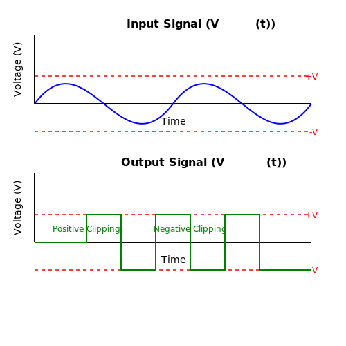
In the realm of signal processing, particularly within electronics and communication, understanding the mechanics of clipping is essential. Clipping occurs when an electronic circuit limits the amplitude of a signal, fundamentally altering the shape of the waveform. This action is typically implemented to protect sensitive components from excessive voltages or currents, ensuring circuit durability and functionality. To delve deeper, clipping can be characterized as the process of "truncating" a waveform, usually a sine wave, at a predefined threshold. When input signal amplitudes exceed this threshold, the circuit effectively "clips" the peaks. The most common form of clipping is hard clipping, where the signal amplitude is abruptly restricted, leading to a distinct alteration in the waveform's characteristics. Conversely, soft clipping allows for a more gradual roll-off, which can yield different harmonic content. The purpose of clipping extends beyond simple signal limitation. It finds extensive applications in various areas including audio processing, where it is used to create distortion effects, often sought after in electric guitar amplifiers. Here, clipping modifies the waveform to add harmonic content that enriches the sound, rendering it more perceptible and aesthetically appealing. Furthermore, clipping demonstrates significant importance in communication systems, where it helps prevent distortion from saturation in receivers, ensuring clear signal transmission and reception. Understanding how to implement clipping effectively requires a grasp of the mathematical fundamentals that govern this phenomenon. Let’s explore the mathematics of clipping. To visualize clipping, imagine a sine wave oscillating between its positive and negative peaks. When applying clipping, we can denote the input signal as \( V_{in}(t) = V_m \sin(\omega t) \), where \( V_m \) is the peak amplitude, and \( \omega \) is the angular frequency. When clipping is applied, the output signal \( V_{out}(t) \) can be mathematically expressed as: $$ V_{out}(t) = \begin{cases} V_{max} & \text{if } V_{in}(t) > V_{max} \\ V_{min} & \text{if } V_{in}(t) < V_{min} \\ V_{in}(t) & \text{otherwise} \end{cases} $$ Here, \( V_{max} \) and \( V_{min} \) represent the clipping thresholds. This piecewise function captures the essence of hard clipping, where the waveform beyond the thresholds does not convey any additional information and simply gets truncated. Visualizing this process, one can imagine the output waveform that retains its form until it reaches defined limits, above which it flatten out into horizontal lines, thus losing the smooth characteristics of the original sine wave. In practical electronics, clipping circuits can be as simple as a diode clipper, where a diode is connected in reverse bias to limit the output voltage to a certain level. Such a configuration effectively prevents the signal from surpassing the diode's forward threshold, thus performing the clipping action seamlessly. In conclusion, understanding clipping is paramount not only for circuit design but also for optimizing performance across various applications in electronics and audio engineering. The knowledge of how signals can be manipulated through clipping enriches both theoretical insights and practical implementations, paving the way for enhancing system robustness and functionality.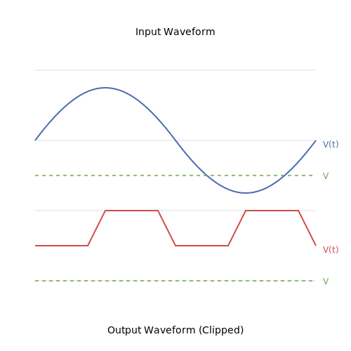
1.2 Types of Clipping Circuits
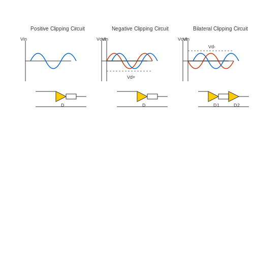
Clipping circuits, an essential aspect of electronic design, serve to limit the voltage levels of a signal to within a specific range, preventing distortion and maintaining signal integrity. There are several types of clipping circuits, each designed to meet particular requirements based on application demands. In this section, we will explore the different types of clipping circuits—specifically, positive clipping circuits, negative clipping circuits, and bilateral clipping circuits.
Positive Clipping Circuits
Positive clipping circuits are designed to clip the positive portion of an input signal while allowing the negative portion to pass unchanged. This is achieved by using a diode oriented to conduct only during the positive half-cycle of the input waveform. When the input voltage exceeds the diode's forward voltage drop, the diode becomes conductive and effectively short-circuits the output, limiting it to approximately zero volts or the diode's forward voltage.
For instance, consider a simple positive clipping circuit consisting of a diode connected in series with a load resistor. When the input voltage exceeds the threshold defined by the diode, the output voltage is clipped. This behavior can be modeled mathematically. If Vin is the input voltage and VD is the diode's forward voltage, the output voltage Vout can be defined as:
This type of circuit is commonly used in audio processing to prevent signal distortion by limiting the maximum amplitude of positive waveforms.
Negative Clipping Circuits
Negative clipping circuits function similar to positive clipping circuits but clip the negative portion of the input signal. Here, the diode is reversed in orientation, conducting during the negative half-cycle of the waveform. This setup allows the positive portion of the input to pass through without modification while limiting the negative component.
The behavior of a negative clipping circuit can also be mathematically modeled. In this case, the output voltage is:
Negative clipping is particularly useful in protecting sensitive electronic components from reverse voltage spikes, such as in relay driving circuits or protection in RF amplifiers.
Bilateral Clipping Circuits
Bilateral clipping circuits are designed to clip both the positive and negative halves of the input signal simultaneously. This configuration can be achieved using two diodes oriented in opposite directions. By clipping both halves, these circuits can be used in applications that require the elimination of signal peaks, such as in data encoding or transmission systems.
The output waveform of a bilateral clipping circuit can be expressed similarly. If we denote the forward voltages of the diodes as VD+ and VD- for the positive and negative diodes, respectively, then:
The practical uses of bilateral clipping circuits include waveform shaping in oscillators and defining voltage limits in signal conditioning applications.
In conclusion, understanding the various types of clipping circuits is vital for engineers and researchers. These circuits play a pivotal role in diverse applications, from audio processing to signal protection, by ensuring that signals remain within desired voltage levels without introducing significant distortion.
1.3 Applications of Clipping Circuits
Clipping circuits, often considered essential in signal processing, exhibit significant versatility across various applications within electronics and engineering. Their ability to selectively limit signal amplitudes without distortion of the waveform makes them invaluable tools in communication systems, audio processing, and even power electronics.Signal Conditioning and Protection
One of the primary applications of clipping circuits is in signal conditioning. Clipping is utilized to protect sensitive components from voltage spikes that could cause damage. For example, in communication systems, clips can prevent high-voltage signals from exceeding the maximum input rating of a receiver. In this context, clamping the signal ensures that any voltage exceeding a defined threshold is diverted or limited, thus preserving the integrity of the crucial components. A practical instance can be observed in the usage of *transient voltage suppressor (TVS) diodes* which clip voltage spikes caused by lightning or electromagnetic interference to protect sensitive equipment. These diodes effectively clamp high-voltage transients, maintaining a safe operating range for downstream components.Waveform Shaping in Audio Applications
In the realm of audio processing, clipping circuits are often employed for waveform shaping, particularly in the development of effects for electric guitars. Here, they can manipulate audio waveforms to enhance harmonic content by intentionally clipping the signal. When an audio waveform exceeds a certain level, clipping the peaks creates harmonic distortion, which can be desirable for producing rich, textured sounds in music. When considering the mathematical implications, a sinusoidal waveform can be expressed as:Integration in Frequency Modulated Systems
Clipping circuits find their applications even in more complex systems such as frequency modulation (FM). In these contexts, clipping can assist in generating a consistent frequency deviation while ensuring signal integrity. In an FM broadcast transmission, for example, clipping can prevent excessive deviations caused by strong audio inputs, ensuring the modulated signal remains within the frequency limits. In terms of modulation, the relationship between the modulating signal \( V_m(t) \) and the carrier signal \( V_c \) can be represented as:Control Systems and Automation
Lastly, clipping circuits are often employed in control systems for analog feedback loops. They are instrumental in preventing oscillation or instability that may arise when control actions exceed limits set by the system constraints. For instance, in automated lighting systems, clipping circuits can ensure that light intensity does not exceed set maximum levels, thus maintaining the system’s overall efficacy. In summary, clipping circuits play a vital role across multiple dimensions of modern electronics — from protecting sensitive components and shaping audio signals to ensuring modulation integrity and enhancing the performance of automated systems. Their diverse applications underscore the importance of understanding clipping behavior in the design and operation of electronic systems. As the technology advances, the integration of clipping circuits with newer digital techniques is likely to create even more sophisticated applications in the future.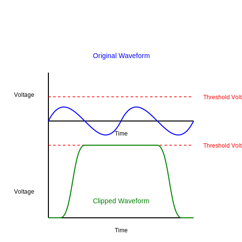
2. Understanding Clamping
2.1 Understanding Clamping
Clamping circuits are integral in the field of electronics, particularly in waveform shaping and protection mechanisms. They serve the essential purpose of transferring a signal's voltage range to a new fixed level, effectively 'clamping' either the positive or negative excursions of the waveform without altering the signal's frequency components. This section delves into the nuances of clamping, exploring its principles, configurations, and applications.
Principle of Clamping
At the core of a clamping circuit lies the distinct difference between clamping and clipping. While clipping circuits limit the voltage peaks of a waveform, often resulting in distortion, clamping circuits shift these peaks to a defined level, maintaining the integrity of the waveform shape but altering its DC level. The basic idea is to adjust the average value of the signal without changing its peak-to-peak value.
Types of Clamping Circuits
Typically, clamping circuits can be classified into two primary types based on the polarity of the operation: positive clamping and negative clamping.
- Positive Clamping: This type of circuit raises the lowest point of the waveform above zero. For instance, if you have an AC signal oscillating between -5V and +5V, a positive clamping circuit could shift this range to 0V to +10V.
- Negative Clamping: In contrast, negative clamping circuits pull the highest point of the waveform down. Using the same AC example, a negative clamp might shift the voltage levels down to -10V to 0V.
Clamping Circuit Configuration
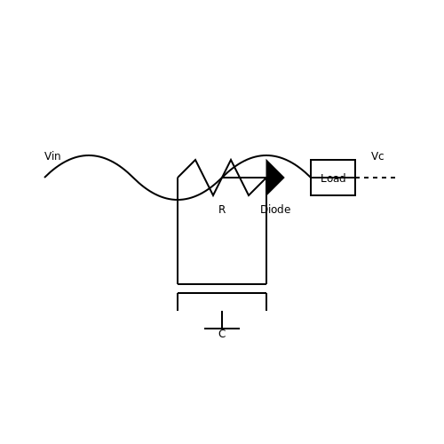
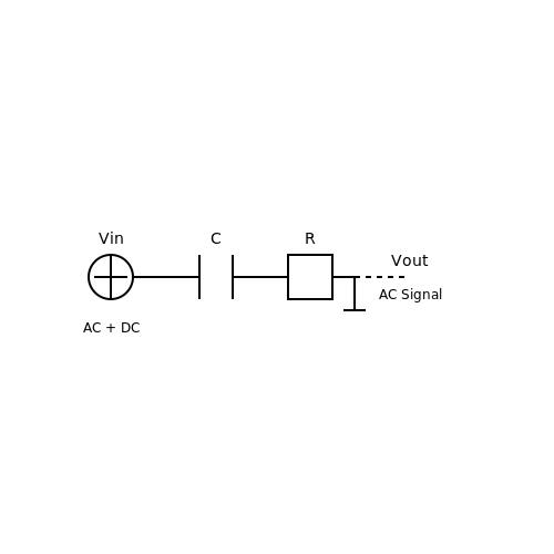
A fundamental configuration for a clamping circuit typically involves a diode, a resistor, and a capacitor. Here is a simplified step-by-step breakdown of the operation:
- The diode allows current to flow in only one direction. During the positive cycle of an input AC signal, the diode conducts and charges the capacitor.
- When the input voltage returns to zero, the capacitor holds its charge. This effectively raises the zero-voltage level of the signal.
- As the AC signal continues to fluctuate, the diode ensures that current can only flow in the intended direction, thus maintaining the desired DC offset while the input waveform retains its original frequency characteristics.
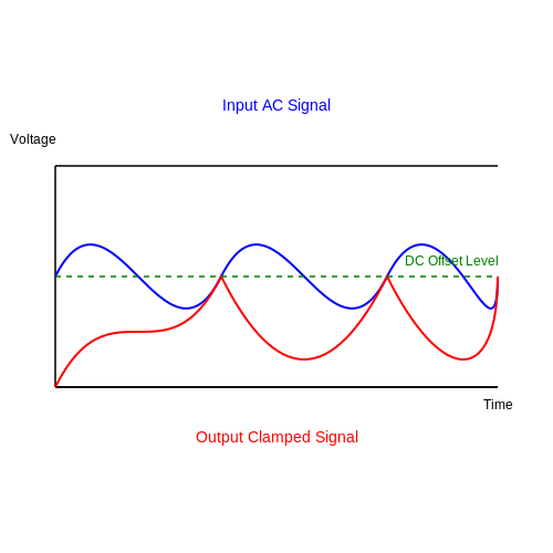
To better understand the functionality of a clamping circuit, consider the following typical waveforms:
Here, \( V_{DC} \) represents the DC level introduced by the clamping action. When applied, \( V_{in} \) oscillates between its inherent values, yet is shifted in the output to reflect a defined DC level.
Real-World Applications of Clamping Circuits
Clamping circuits are used extensively in various applications:
- Signal Conditioning: Used in sensors to ensure the output meets specific voltage levels for subsequent processing.
- Waveform Shaping: In audio or RF circuits, clamping is crucial to prevent high voltage spikes from damaging sensitive components.
- Protection Circuits: Employed in surge protection to inhibit excess voltage from reaching load components.
Overall, the ability of clamping circuits to maintain signal integrity while modulating DC levels is a powerful tool for electrical engineers addressing complex signal processing tasks.
2.2 Types of Clamping Circuits
Clamping circuits serve vital roles in electronics, primarily by shifting the DC level of an AC signal without altering its shape. This section will explore various types of clamping circuits, each with unique characteristics and applications, enhancing your understanding of how these circuits can be employed in practical scenarios.
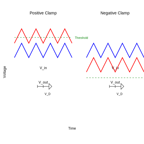
Positive Clamping Circuits
Positive clamping circuits elevate the lowest point of an input signal to a predefined higher voltage level. This functionality is crucial in circuits where negative voltages can cause damage to sensitive components or lead to unsatisfactory performance. Typically, a diode and a capacitor are used in conjunction to create a positive clamp.
In operation, the diode conducts and charges the capacitor when the input signal is positive. Once the capacitor is charged, the diode becomes reverse-biased when the input signal swings negative, holding the output at the desired clamped level. The phase shift isn't recommended for precise signal processing but is ideal for protecting devices from negative excursions.
The above equation illustrates that the output voltage is equal to the input voltage plus the forward voltage drop of the diode, \( V_{D} \). This simple relationship highlights the practical importance of the diode's characteristics in determining the clamped output level.
Negative Clamping Circuits
Negative clamping circuits essentially perform the opposite function of their positive counterparts. They ensure that the highest point of the input signal does not exceed a specific negative voltage level, thereby preventing the signal from dropping below this threshold.
Constructed similarly to the positive clamp, negative clamping circuits use a diode, but in this case, the diode's anode is connected to ground while the cathode is connected to the output. When the input goes beyond the negative threshold, the diode conducts to ground, clamping the output voltage.
This equation illustrates the output voltage of the negative clamp, demonstrating that it is equal to the input voltage minus the diode's forward voltage drop. Such circuits are invaluable in protecting amplifiers and other sensitive components from overranging negative potentials.
Biased Clamping Circuits
In certain scenarios, using a fixed clamping threshold capacitor alone may not suffice, particularly where dynamic adjustments are necessitated by varying input signals. Biased clamping circuits introduce an additional voltage reference, often sourced from another power supply voltage, effectively allowing for more precise control over the clamping level.
By connecting a resistor from the reference voltage to the diode, designers can control how the circuit behaves under various signal conditions. This feature is particularly useful in communication systems where the signal characteristics may fluctuate significantly, rendering standard clamps ineffective.
An Example Application: Signal Conditioning in Audio Processing
One practical application of biased clamping circuits is in audio processing, where maintaining signal integrity while preventing distortion is paramount. Here, they can be integrated into audio signal processing chains to ensure that the output levels are maintained within desired limits, enhancing sound clarity and preventing damage to speakers from overdriven signals.
Summary
The variety of clamping circuits—positive, negative, and biased—allowed designers to secure and manipulate signals effectively in various electronic applications. Understanding these circuits' operational principles is critical for any engineer aiming to master advanced electronics or design robust systems that require precision voltage management.
2.3 Use Cases for Clamping Circuits
In the realm of electronics, clamping circuits play a crucial role in protecting sensitive components and enabling signal processing strategies. These circuits, which limit the voltage to a specific range by "clamping" excess voltages to predefined levels, find extensive applications across various fields. Understanding their use cases not only emphasizes their importance but also provides insight into their design choices and operational efficacy.Signal Conditioning
One of the primary applications of clamping circuits is in signal conditioning. In systems where analog signals are prone to interference or noise, clamping circuits help in maintaining signal integrity. For example, in an analog-to-digital conversion process, clamping circuits can ensure that the input signal remains within the operational limits of the ADC, thus preventing distortion or inaccurate readings. These circuits are especially valuable in mixed-signal systems where digital and analog components coexist, as they can effectively isolate noisy segments.Voltage Protection
Clamping circuits are widely utilized for protecting sensitive devices and systems from voltage spikes, such as those produced by inductive loads or switching devices. In practical settings, transistors, integrated circuits, and microcontrollers can suffer severe damage if subjected to excessive voltages. By using clamping diodes in conjunction with inductive components, one can create a robust design that mitigates high-voltage transients, ensuring longevity and reliability in various applications, from automotive electronics to telecommunications.Waveform Shaping
Another intriguing use case for clamping circuits is waveform shaping. In signal processing applications, clamping circuits are often employed to modify the shape of a waveform for further processing or interfacing with other systems. For instance, in pulse-width modulation (PWM) systems, clamping circuits can adjust the duty cycle of a PWM signal by effectively limiting peak voltage levels. This capability is especially valuable in applications such as motor control or LED dimming, where an accurate modulation of voltage is required for optimum performance.Data Transmission and Communication
In communication systems, maintaining signal levels is essential for reliability and efficiency. Clamping circuits help preserve the integrity of transmitted signals by ensuring that they remain within the bandwidth limits of the communication channel. For instance, in high-speed data lines, voltage clamping can prevent signal degradation due to reflection or crosstalk, thus enhancing overall data transmission fidelity. This application is critical in fiber optic communications, where even slight voltage variations can lead to significant data loss.Interfacing with Sensors
Sensors, particularly those that generate low-level signals, require precise clamping to avoid damage from overvoltage conditions. Many sensors, such as thermocouples and photodetectors, provide analog output signals that fall within very specific electrical ranges. Utilizing clamping circuits allows engineers to safely interface these sensors with microcontroller inputs without risking damage. By doing so, clamping circuits provide an automatic safeguard mechanism that complements the design of sensor-based systems.Case Study: Overvoltage Protection in Automotive Electronics
A prime example of clamping circuits in a real-world application can be observed in the automotive industry. Vehicles today are loaded with electronic systems—from engine control units to advanced driver-assistance systems (ADAS)—that are sensitive to voltage levels. In these environments, sudden voltage spikes can arise due to load dump events or transient responses. Implementing clamping diodes within circuit designs protects critical components by redirecting excess voltage away from sensitive parts, thereby reducing failure rates and ensuring reliable car operation. The diversity of use cases for clamping circuits illustrates their fundamental role in modern electronic and electrical systems. As technology evolves, the continued integration of clamping circuits will be vital to ensuring the performance, durability, and safety of electronic devices across a wide array of industries.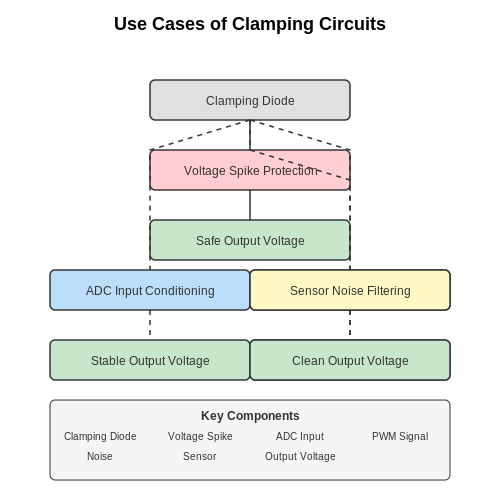
3. Diode Clipping Circuits
3.1 Diode Clipping Circuits
Diode clipping circuits are fundamental components in analog electronics, providing the ability to restrict the amplitude of a signal to a specific range. This process is crucial in preventing signal distortion and protecting components in various electronic applications. By understanding the operating principles of diode clipping circuits, engineers can effectively tailor signals for multiple purposes, including audio processing, signal modulation, and waveform shaping.
Principle of Operation
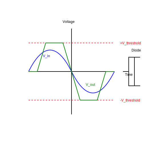
The fundamental principle behind a diode clipping circuit lies in the diode's inherent characteristics, notably its forward and reverse bias conditions. A diode allows current to flow predominantly in one direction, thereby "clipping" the waveform when the signal exceeds a set threshold. In essence, this behavior can be utilized to remove portions of the waveform outside a designated amplitude limit.
A simple diode clipping circuit typically consists of a diode connected in series or parallel with the load, influenced by its orientation:
- Positive clipping: When the input signal exceeds a specific positive voltage, the diode conducts and "clips" off the excess voltage.
- Negative clipping: Likewise, if the input signal goes below a defined negative voltage, the diode conducts in the reverse direction, clipping the lower portion of the waveform.
Mathematical Modelling
To further clarify how diode clipping works, we can analyze the voltage across the load, denoted as $$V_{out}$$. Assuming a sinusoidal input voltage $$V_{in}$$ described by:
where $$V_m$$ is the peak voltage and $$\omega$$ is the angular frequency. Let's denote the clipping threshold voltage as $$V_{threshold}$$. As the input varies with time, the output can be expressed as follows:
For positive clipping:
Similarly, for negative clipping:
Real-World Applications
Diode clipping circuits are employed in various real-world applications:
- Audio Processing: Clipping circuits are widely used in audio systems to prevent distortion and protect speakers from over-voltage conditions.
- Signal Conditioning: They are crucial in shaping signals in communication systems to ensure clean transitions and prevent interference.
- Voltage Protection: Diode clamps safeguard sensitive electronic components from voltage spikes, improving reliability in power management systems.
Understanding and designing effective diode clipping circuits can significantly enhance the performance and durability of many electronic devices. As technologies advance, the integration of these circuits into sophisticated electronics continues to evolve, providing exciting opportunities for innovation in signal processing and electronics.
3.2 Transistor-Based Clipping Circuits
Transistor-based clipping circuits are pivotal in shaping waveform signals within electronic systems. By utilizing transistors, these circuits can clip or limit the voltage peaks of an input signal, thus preventing distortion in subsequent analog and digital processing stages. This capability is vital in applications ranging from signal conditioning to creating audio waveforms in synthesizers.
At a fundamental level, clipping occurs when the signal exceeds a predefined threshold, resulting in a flattened waveform. When implemented through transistors, the clipping function can be finely tuned, allowing engineers to adjust the circuit’s response characteristics effectively.
Operational Principles
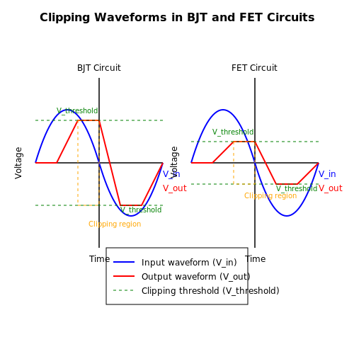
Transistor clipping circuits usually employ either BJTs (Bipolar Junction Transistors) or FETs (Field-Effect Transistors). The choice between these devices influences the circuit’s linearity, frequency response, and the amount of clipping achieved. In essence, the transistors operate as electronic switches that activate at certain input voltage levels.
BJT Clipping Circuit
In BJT-based clipping circuits, the configuration typically involves using transistors in a common emitter or common base arrangement. When the input voltage exceeds the base-emitter voltage threshold (approximately 0.7V for silicon BJTs), the transistor begins to conduct, effectively 'clipping' the positive peaks of the waveform. For negative peaks, a diode may be placed in reverse bias to limit the amplitude below ground potential.
This equation succinctly explains how voltage levels behave in a simple clipping circuit: V_{threshold} represents the set clipping threshold. This linear piecewise function showcases the circuit's ability to retain signal integrity below the threshold while clipping the higher amplitudes.
FET Clipping Circuit
When employing FETs, a similar principle applies, though the control of the gate voltage introduces additional flexibility. With JFETs (Junction Field Effect Transistors), for example, increasing the gate-source voltage allows for a better adaptation of the clipping limit. This can yield a much smoother transition as the gate bias interacts with the input waveform.
In the equation above, R_d represents the drain resistor, while R_g denotes the gate resistor. Adjusting these resistances alters the clipping threshold, thereby facilitating customized applications depending on the required performance. Such configurations are immensely useful in audio processing, where preserving fidelity despite signal level fluctuations is essential.
Applications and Practical Considerations
Transistor-based clipping circuits find their niche in various fields. In audio electronics, they serve to limit the amplitude of sound signals, preventing distortion that could result from high peaks. Similarly, in telecommunications, these circuits ensure signals remain within operable ranges before modulation and transmission.
The design of clipping circuits must also account for device saturation and signal integrity. Excessive clipping may lead to undesired harmonics, introducing distortion rather than mitigating it. Consequently, careful simulation and testing are often required to define optimal operating conditions.
In addition to analog signal processing, transistor clipping circuits are pivotal in digital systems, where pulsating signals must be kept within logic levels to avoid erroneous data interpretation. Employing precise and reliable transistor-based clipping circuits ensures the digital environment functions flawlessly in tandem with its analog counterparts.
To summarize, understanding the functional mechanics of transistor-based clipping circuits is crucial for engineers and researchers focused on signal processing. The ability to tailor these circuits not just makes them powerful tools but also enables engineers to explore innovative solutions within their projects.
3.3 Simulating Clipping Circuits using SPICE
In the realm of electronics, clipping circuits play a crucial role in shaping signals, particularly in audio processing and communication systems. These circuits limit the amplitude of a signal to a specific level, preventing distortion and saturation. With the advent of simulation tools such as SPICE (Simulation Program with Integrated Circuit Emphasis), engineers can model and analyze the behavior of clipping circuits more efficiently. This section aims to guide you through the process of simulating clipping circuits using SPICE, emphasizing both practical approaches and theoretical foundations.
Understanding Clipping in Circuit Design
Clipping occurs when the amplitude of an input signal exceeds the thresholds set by the circuit elements, leading to parts of the waveform being “clipped” off. In SPICE simulations, two common types of clipping circuits—hard clipping and soft clipping—can be easily constructed and tested. Hard clipping abruptly removes the peaks of the waveform, resulting in a rectangular output shape, while soft clipping smoothly transitions from linear to saturated output, creating a more gradual response.
Preparing the SPICE Simulation Environment
Before diving into the clipping circuit simulation, it is critical to set up the SPICE environment accurately. This includes defining the appropriate models for the components used, such as diodes, resistors, capacitors, and operational amplifiers. For instance, accurate diode models should be sourced from the SPICE library to simulate their forward voltage drop and reverse recovery time.
Implementing a Basic Hard Clipping Circuit
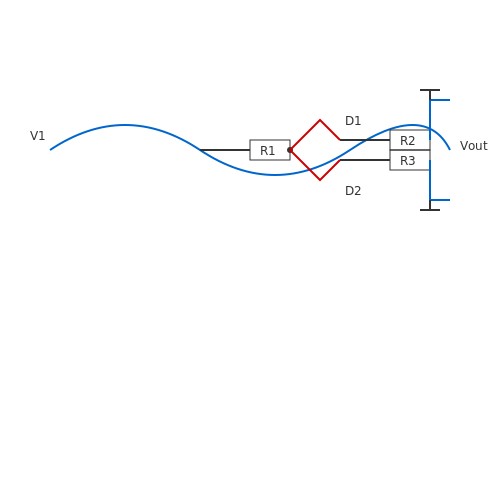
To create a simple hard clipping circuit using diodes and resistors, consider the circuit shown below. It consists of an input sine wave signal, connected to a resistor leading to two diodes oriented in opposite directions. Each diode clips the signal on either side of the zero voltage, effectively limiting it to a specific amplitude.
In this scenario, \(V_D\) is the forward voltage drop across the diode. The equation describes how the output voltage responds to varying input voltages, effectively modeling the action of a hard clipping circuit.
Example SPICE Code for Hard Clipping Circuit
* Hard Clipping Circuit in SPICE Simulation
V1 IN 0 SINE(0 1 1k)
R1 IN N1 1k
D1 N1 N2 D
D2 N1 N3 D
R2 N2 OUT 1k
R3 N3 OUT 1k
.model D D(IS=1e-12)
.tran 0 10ms
.end
In this SPICE code:
- V1: Defines a sine wave voltage source (1V amplitude, 1kHz frequency).
- R1: Resistor connected to the input.
- D1 and D2: Diodes for hard clipping.
- R2 and R3: Resistors that help to create the output path.
Analyzing the Output Waveform
After running the simulation, you can visualize the output waveform, which should demonstrate the characteristic clipped signal. Analyzing the output allows for parameter adjustments, including resistor values and diode characteristics to optimize performance depending on application requirements.
Soft Clipping Circuit Simulation
Soft clipping circuits can be simulated with a similar setup, but involving components such as operational amplifiers configured in feedback loops. The feedback network will determine the clipping characteristics to enhance signal integrity.
Simulation tools like SPICE provide the flexibility to play with component values and configurations in real time, leading to more efficient design iterations. This hands-on approach not only enhances understanding but also leads to practical implementations in real-world circuits.
As we dive deeper into SPICE simulations, the principles learned in this section will lay the groundwork for more complex circuit topologies involving clamping effects, dynamic range processing, and signal conditioning.
4. Diode Clamping Circuits
4.1 Diode Clamping Circuits
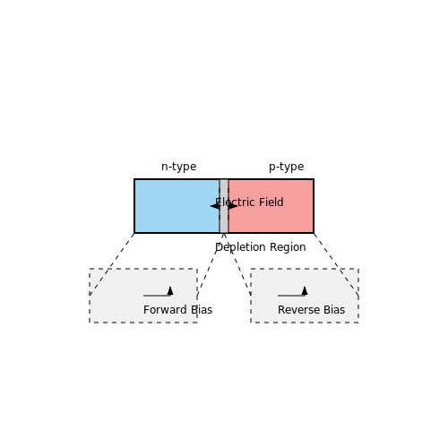
Diode clamping circuits play an essential role in electronic systems, particularly in signal processing and waveform shaping applications. At their core, diode clamping circuits allow the alteration of input waveforms by fixing a certain level of voltage, thereby "clamping" the waveform to a specified reference level. This functionality has numerous applications, such as protecting sensitive electronic components from voltage spikes and modifying signal levels for compatibility with other devices. To understand the fundamentals of diode clamping circuits, we first need to review the behavior of diodes in a forward and reverse-biased state. A diode permits current to flow predominantly in one direction, characterized by its forward voltage drop (typically around 0.7 V for silicon diodes). When reverse-biased, the diode blocks current flow until the reverse breakdown voltage is reached. This behavior is leveraged in clamping circuits to shape input waveforms. The primary types of diode clamping circuits include positive clamping and negative clamping configurations. Both utilize diodes but differ in their output characteristics.Positive Clamping Circuit
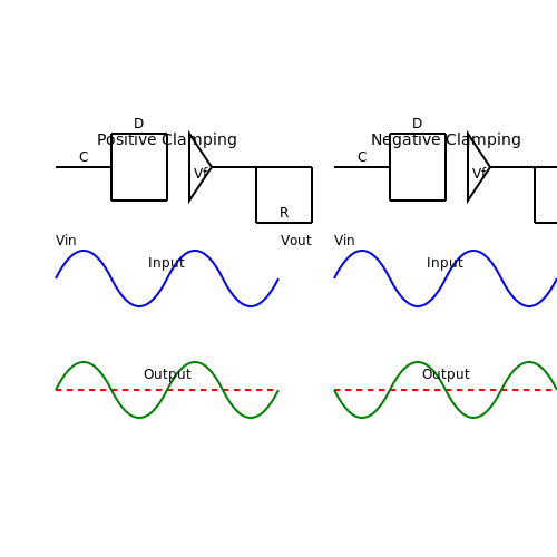
In a positive clamping circuit, a diode is forward-biased, allowing the output voltage to rise above the ground level. Typically, the circuit consists of a diode, a resistor, and a capacitor connected in series, with the input signal applied across the combination. When the input signal surpasses the diode's forward voltage, it clamps the output to a level approximately equal to the input voltage minus the diode's forward voltage drop. Let's define the circuit with an input voltage \( V_{in} \), a capacitor with capacitance \( C \), and a resistance \( R \). By analyzing the behavior of a simple positive clamping circuit through the following methods, we can derive its characteristics: 1. Initial Condition: When the input voltage is zero, the capacitor is uncharged, and the output voltage \( V_{out} \) is also zero. 2. Positive Cycle: As the input voltage rises, it exceeds the diode's forward voltage. When this occurs, the diode conducts, and the output voltage follows the input with a drop corresponding to the forward voltage \( V_f \). The relationship can be defined as: $$ V_{out} = V_{in} - V_f $$ In steady-state conditions, if the input is a sine wave, the output will be a sine wave clamped at \( V_f \).Negative Clamping Circuit
Conversely, a negative clamping circuit shifts the entire waveform downwards. Here, the diode operates in a reverse-biased mode while the capacitor captures the input signal levels. In this arrangement, the diode effectively 'clamps' the negative peaks of the input signal, holding the output voltage at a defined negative level. Following similar analytical steps as before, we can express the output voltage in this case as: 1. Negative Cycle: The diode becomes forward-biased when the input goes below a defined value (typically ground). The output can be determined as: $$ V_{out} = V_{in} + V_f $$ Consequently, the output level will now reflect lower levels of the input waveform, accommodating the negative shift.Practical Relevance and Real-World Applications
Diode clamping circuits are utilized in various applications, including:- Signal Protection: These circuits effectively prevent voltage transients from damaging sensitive electronic components.
- Signal Conditioning: They prepare signals for processing by ensuring appropriate levels before transmission in communication systems.
- Waveform Shaping: In generating pulse-width modulation (PWM) signals, clamped outputs allow for controlled waveform durations and amplitudes.
- Level Shifting: They enable shifting signals into the operational range of receiving circuitry, crucial in mixed-voltage environments.
4.2 Active Clamping Circuits
In electronic circuits, clamping techniques are essential for protecting components and ensuring signal integrity. Active clamping circuits take this further by leveraging active components to establish precise voltage thresholds while allowing for signal restoration. This subsection delves into the principles, implementations, and applications of active clamping circuits, highlighting their advantages over passive systems.Understanding Active Clamping Circuits
An active clamping circuit typically employs transistors or operational amplifiers to control the voltage levels in a circuit. Unlike passive clamping techniques, which rely on diodes, active circuits can be more finely tuned to respond to varying conditions. The core functionality hinges upon the feedback mechanisms of the active components, which allow the circuit to maintain desired output levels despite fluctuations in input signals.Basic Working Principle
The essence of an active clamping circuit lies in its ability to adjust the clamping voltage dynamically. This can be expressed mathematically. Let’s consider a simple active clamp configuration using an operational amplifier. The relationship between the input (V_in), output (V_out), and the feedback resistor (R_f) can be described using Ohm's law and the principles of feedback. For example, if a voltage is applied across a feedback resistor, the operational amplifier can react to limits set by its power supply and input thresholds. 1. Standard feedback mechanism gives: $$ V_{out} = \left( \frac{R_f}{R_f + R_{in}} \right) V_{in} $$ 2. In clamping mode, we set a reference voltage (V_ref) using zener diodes or similar components leading to: $$ V_{out} = V_{ref} + (V_{in} - V_{ref}) \cdot \text{gain} $$ This dependency showcases how voltage clamping can actively adjust based on input, offering a more effective solution than passive clamps.Key Advantages of Active Clamping
Active clamping circuits boast several benefits:- Dynamic Adjustment: They can adjust clamping levels based on the input rather than being fixed, as is often the case with passive designs.
- Increased Speed: Active components operate faster than passive ones, allowing for better handling of high-frequency signals.
- Precision: They can maintain tighter tolerances for clamping voltages, critical in sensitive applications.
- Versatility: Various circuit topologies can be adapted for different requirements—useful in power management and signal processing.
Applications of Active Clamping Circuits
The applications of active clamping circuits span a multitude of fields. Some notable examples include: 1. Transient Voltage Suppression: Active clamping circuits are essential in protecting sensitive electronics from voltage spikes caused by surges in electrical systems. 2. Signal Conditioning: Used in analog signal processing, these circuits ensure that signals remain within acceptable voltage levels, preventing distortion or loss of information. 3. Over-Voltage Protection in Power Circuits: Active clamps can dynamically adjust to protect circuit elements during over-voltage scenarios, which may occur in power distribution networks. 4. Data Communication: In communication systems, they help in stabilizing voltage levels, ensuring consistent performance and integrity of the transmitted data. The exploration of active clamping circuits provides significant insight into how modern electronic designs manage voltage and ensure reliability. As systems become more complex, the importance of such technology in safeguarding and optimizing performance continues to grow.4.3 Simulating Clamping Circuits using SPICE
Clamping circuits serve as essential tools in electronics for controlling signal levels and protecting sensitive components. This section will delve into the practical simulation of clamping circuits using SPICE, a widely used simulation tool in the engineering domain. SPICE provides an efficient and powerful platform for both analysis and visual interpretation of circuit behavior before physical implementation.
Understanding SPICE Simulation Basics
SPICE, an acronym for Simulation Program with Integrated Circuit Emphasis, is a cornerstone in electronics design, enabling engineers to simulate the behavior of analog and digital circuits under various conditions. With SPICE, users can model voltage, current, and various other metrics in an electronic circuit. Utilizing netlists, SPICE employs a high-level, textual representation of the circuit, which is parsed and simulated to reveal circuit responses.
Before diving into clamping circuit simulations, it’s pivotal to comprehend the basics of creating a SPICE netlist. A netlist works as a blueprint of your circuit, stating components and their interconnections. Each component in SPICE is identified by a unique node and has predefined models, like resistors (R), capacitors (C), diodes (D), and operational amplifiers (U).
Designing a Simple Clamping Circuit
Let’s consider a simple clamping circuit that shifts the voltage level of an input sine wave signal. In this particular example, we will use a diode as the clamping device to shift the signal upwards, essentially clamping it at a specific DC level.
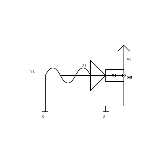
The schematic of the circuit consists of:
- A sinusoidal voltage source (e.g., V1).
- A diode (e.g., D1).
- A resistor to limit current through the diode (e.g., R1).
- A DC voltage source to adjust the clamping level (e.g., V2).
SPICE Netlist Example
The following is a standard netlist for the described clamping circuit:
* Simple clamping circuit simulation
V1 in 0 SIN(0 5 1k)             ; Sine wave source: 5V amplitude, 1kHz frequency
D1 in out D                     ; Diode model
R1 out 0 1k                     ; Resistor value of 1k ohm
V2 out 0 2                      ; DC voltage source: 2V upshift

.model D D(IS=1e-14)            ; Diode characteristics
.tran 0.1ms 5ms                ; Transient analysis from 0 to 5ms
.end
This netlist defines a simple clamping circuit in which a sine wave voltage source is clamped at 2 volts. The diode model specified includes saturation current characteristics to provide realistic behavior during simulation. The transient analysis command simulates the wave's behavior over time, allowing us to verify the circuit's functionality.
Running the Simulation
To execute the simulation, load the netlist into your SPICE environment and run the transient analysis. Observe the output waveform at the node defined by out. You should see the input sine wave adjusted such that its minimum value aligns with the clamping level imposed by the DC voltage source.
This process not only validates the operational principles of a clamping circuit but also allows for design refinements based on simulation behavior. Engineers often leverage this ability to iteratively design and troubleshoot circuits before deployment in real-world applications, ranging from audio processing to signal conditioning in sensors.
Conclusion
Simulating clamping circuits using SPICE provides a hands-on experience that fosters deeper understanding and mastery of electronic design principles. As clamping circuits have numerous real-world applications—from protecting amplifiers from voltage spikes to shaping signal levels—a solid grasp of their behavior through simulation underpins effective engineering practice. As you explore further, consider the implications of different component choices and the interplay between circuit dynamics and system performance.
5. Component Selection and Specifications
5.1 Component Selection and Specifications
In the realm of applied clipping and clamping circuits, the selection of components is pivotal in achieving desired performance metrics. Each component in these circuits serves a specific purpose, influencing factors like voltage levels, current handling, and overall circuit robustness.Understanding Component Roles
To efficiently design clipping and clamping circuits, we must first understand the roles of key components. The fundamental building blocks generally include diodes, resistors, capacitors, and operational amplifiers (op-amps). Each component’s specifications directly correlate with circuit outcomes, particularly in terms of speed (response time), efficiency, and thermal stability.Diodes: The Heart of Clipping Circuits
Diodes are critical in determining the clipping levels of a circuit. When selecting a diode, consider the following specifications:- Forward Current Rating (IF): This indicates the maximum current the diode can handle without degradation. For clipping applications, ensure your diodes exceed the peak current experienced in your circuit.
- Reverse Voltage Rating (VR): This defines the maximum voltage the diode can withstand in the reverse bias condition. It should be higher than the maximum expected reverse voltage in the circuit.
- Speed (trr): The recovery time of the diode is crucial in high-frequency applications. Schottky diodes offer lower forward voltage drop and quicker recovery times than standard PN junction diodes, making them excellent for rapid switching.
Resistors and Current Limiting
Resistors play a crucial role in shaping circuit characteristics. Key points include:- Resistance Value (R): The resistance value determines the amount of current flowing through the circuit during operation. Choose values to meet desired performance without exceeding power ratings.
- Power Rating (PR): Ensure the resistor can dissipate heat generated due to current flow. The power rating can be calculated with \( P = I^2R \), where I is the circuit current.
Capacitors: Stabilization and Energy Storage
Capacitors are essential for stabilizing voltage levels and providing energy storage. Consider the following:- Capacitance Value (C): The capacitance in microfarads (µF) affects response time. Higher values can respond to low-frequency signals, but may introduce delay to high-frequency signals.
- Voltage Rating (VC): Similar to diodes, ensure your capacitor can withstand maximum circuit voltages without breakdown.
Operational Amplifiers: Precision Control
Op-amps, typically employed in advanced clamping applications, enable precise voltage manipulation. While selecting op-amps, focus on:- Offset Voltage (VOS): A lower offset voltage enhances accuracy in applications where precision is vital.
- Gain Bandwidth Product (GBP): This defines how well the op-amp can respond to high-frequency signals. Higher values are advantageous for circuits processing rapid signal changes.
Conclusion
In summary, the selection of components for applied clipping and clamping circuits significantly impacts the functionality and reliability of the circuit. Understanding the key specifications and characteristics of each component will enable engineers and researchers to design effective solutions tailored to specific applications. This thoughtful approach to component selection lays the groundwork for successful circuit performance across various domains, from signal processing to power management.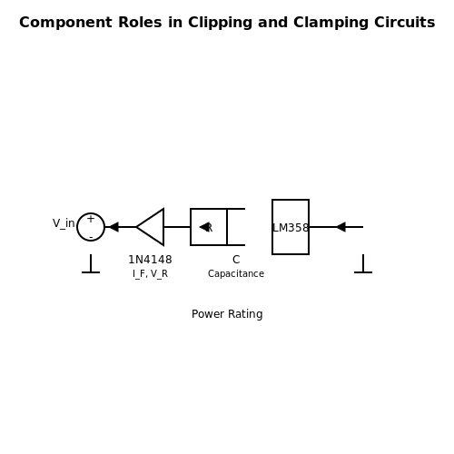
5.2 Troubleshooting Common Issues in Clipping and Clamping Circuits
Clipping and clamping circuits play critical roles in signal conditioning, particularly in protecting sensitive components and managing signal levels. However, like any circuit, they can present challenges when not performing as expected. Understanding common issues and their resolutions can save time and increase the reliability of your applications.
Understanding Circuit Behavior
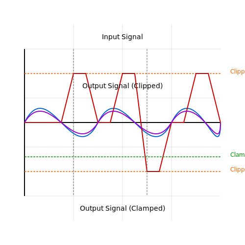
Before diving into troubleshooting, it is essential to have a solid grasp of how clipping and clamping circuits operate. Clipping circuits limit the voltage levels of a waveform by cutting off (or "clipping") parts of the signal that exceed a predefined threshold. Conversely, clamping circuits shift the waveform vertically without altering its shape, ensuring it remains within desired voltage bounds. Each circuit's performance heavily relies on component selection, configuration, and surrounding conditions.
Common Issues and Their Solutions
Here are some prevalent issues encountered in clipping and clamping circuits, along with practical solutions:
- Insufficient Clipping: If the circuit fails to clip sufficiently, the threshold may need adjustment. Verify that the zener diodes or operational amplifiers are within their rated specifications. For zener diodes, ensure that the breakdown voltage is correctly chosen and matches your design parameters.
- Hyper Clipping: Conversely, too much clipping can distort the waveform excessively. In such cases, review your resistor and capacitor values as well as the power supply levels. Adjustments here can help position the clipping threshold more appropriately in relation to the input signal.
- Noise Issues: Excessive noise can introduce fluctuations in the base level of the output signal, particularly problematic with clamping circuits. Minimize noise by evaluating the layout and considering components with lower noise ratings. Employing bypass capacitors on power feeds can also mitigate noise-induced variations.
- Slow Response Time: Slow circuit response can occur due to large capacitive elements or high resistance values. To troubleshoot, consider lowering capacitance or resistance until you find a suitable balance between performance and expected behavior, keeping in mind the impact on the overall circuit behavior and phase shift.
Practical Testing Techniques
To effectively diagnose issues, utilize tools such as oscilloscopes and multimeters. Firstly, observe the output waveform. An oscilloscope allows you to visualize clipping levels and dynamic shifts in output voltage. Compare the input versus the output to identify discrepancies that reveal circuit behavior. You can take measurements at various points including the input, the output, and the key nodes around your clipping or clamping components.
Always check voltages using a multimeter to ensure they align with expected thresholds. For clamping circuits, confirm that the reference voltage aligns with theoretical designs, ensuring you account for component tolerances that can influence circuit performance.
Case Study: Real-world Application
A practical demonstration of troubleshooting can be linked to its application in audio processors. In signal processors, improper clipping can lead to harsh distortion or an overly soft dynamic range. By carefully adjusting the clipping levels and utilizing real-time testing with an oscilloscope during live audio processing, engineers can achieve optimal performance and preserve signal integrity while preventing damage to equipment.
In summary, while clipping and clamping circuits can present various challenges, understanding their mechanics and employing systematic troubleshooting techniques greatly enhances the reliability and performance of these circuits in real-world applications.
5.3 Testing and Validation Methods
In the realm of applied clipping and clamping circuits, rigorous testing and validation are imperative to ensure performance consistency and reliability in real-world applications. These circuits serve crucial purposes in signal processing, protection against voltage transients, and waveform shaping, making their accurate functionality vital for engineers and designers.
Fundamentally, the testing and validation of clipping and clamping circuits revolve around specific methodologies that assess both the electrical characteristics and performance under varied operating conditions. We will delve into three principal testing and validation methods: visual inspection, functional testing, and performance evaluation.
Visual Inspection
Visual inspection serves as the initial stage of the validation process. This method involves a thorough examination of the physical components of the circuit, including:
- Component Integrity: Checking for signs of damage, corrosion, or incorrect soldering of components.
- Layout Verification: Ensuring the circuit aligns with the schematic design and adheres to best practices in PCB layout.
- Grounding and Shielding: Verifying appropriate grounding and shielding techniques are in place to minimize interference.
Although visual inspection cannot fully validate circuit performance, it plays a critical role in identifying potential issues that may affect functionality.
Functional Testing
After visual verification, functional testing aims to observe how well the clipping and clamping circuits perform under expected operating conditions. This involves:
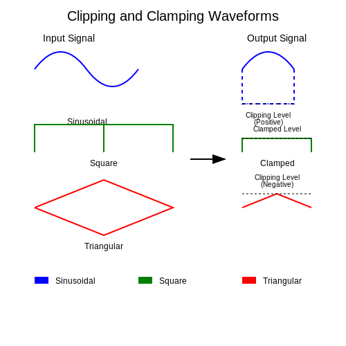
- Input Signal Testing: Generating known input signals (sinusoidal, square, triangular) to evaluate how the circuit responds. A function generator is often employed for this purpose.
- Output Measurement: Using an oscilloscope to observe output waveforms, comparing them against theoretical expectations based on the circuit's design.
Functional testing can reveal whether the circuit effectively clips or clamps signals as intended. Pay special attention to parameters such as clipping levels and distortion—parameters that can impact signal integrity.
Performance Evaluation
Performance evaluation assesses the circuit's behavior concerning various environmental factors, including temperature, frequency, and load conditions. This method can be broken down into the following:
- Temperature Testing: Ensuring that the circuit operates effectively within its specified temperature range. Components may differ in performance at temperature extremes.
- Frequency Response Testing: Evaluating how clipping and clamping circuits behave over a range of frequencies ensures they maintain performance in a real-world context.
- Load Conditions: Testing the circuit under varying load conditions to ascertain stability and robustness in practical applications.
To document the findings from performance evaluations, engineers often utilize standard testing equipment, encompassing multimeters, oscilloscopes, and specialized signal analyzers. Following performance evaluation, comparative analysis against theoretical models or simulations can provide insights into discrepancies and areas for improvement.
In summary, effective testing and validation methods for applied clipping and clamping circuits are critical not only in ensuring component reliability but also in verifying the operational integrity under various conditions. By adhering to these methodologies, engineers can achieve a more robust and dependable design, ultimately enhancing the circuit's application in complex electronic systems.
6. Integrating Clipping and Clamping Circuits in Applications
6.1 Integrating Clipping and Clamping Circuits in Applications
In modern electronics, clipping and clamping circuits play an indispensable role in signal processing and waveform shaping. Their effective integration into various applications enables engineers and researchers to manipulate signals in ways that enhance performance and functionality. ### Understanding Clipping and Clamping Before diving into applications, it's crucial to clarify the meanings of clipping and clamping. Clipping circuits are essential for limiting the amplitude of a signal, effectively cutting off parts of the waveform that exceed a certain voltage level. This is frequently performed using diodes, which conduct current in one direction and prevent it from exceeding specified limits, acting as voltage clamps at the output. On the other hand, clamping circuits shift the entire waveform up or down without altering its shape, introducing a DC offset. This function is typically accomplished with the help of capacitors and diodes, which temporarily hold the charge during the signal's transition, effectively altering the baseline voltage of the output signal. ### Real-World Applications The practical applications of clipping and clamping circuits are both numerous and varied, spanning across different fields of technology. Below are several key examples: #### 1. Signal Conditioning in Audio Equipment In audio processing, clipping circuits are routinely integrated to avoid distortion that can occur when audio signals exceed the maximum capabilities of amplification stages. By utilizing diode-based clipping, engineers can ensure signals remain within acceptable levels without losing essential musical details. #### 2. Voltage Regulation in Power Supplies Clamping circuits find extensive use in power supply systems, especially in transient voltage suppression. By using clamp circuits to divert excess voltage to ground (or another path), sensitive components are protected from voltage spikes that could cause catastrophic failures. #### 3. Data Transmission In communication systems, clamping is crucial for aligning signal levels before transmission to maintain reliability. For instance, clamping circuit techniques are beneficial in pulse signal systems (like UART), where it is essential to maintain a standard logic level relative to ground. #### 4. Waveform Shaping in Oscillators For oscillator circuits, clipping can create square waves from sine waves, transforming output waveforms in a manner suitable for digital electronics. This transformation is vital in frequency generation and clock signal creation in microcontrollers and digital systems. ### Mathematical Modeling To illustrate how these circuits can be quantitatively assessed, let us derive the behavior of a simple diode clipping circuit. Consider a steady input voltage \( V_{in} \) applied to a diode. When the input exceeds a certain threshold voltage \( V_{D} \) (the diode's forward voltage drop), the output waveform \( V_{out} \) can be modeled as: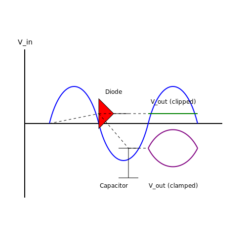
6.2 Influence of Load Conditions on Circuit Performance
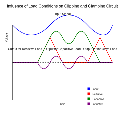
In the context of applied clipping and clamping circuits, understanding how load conditions affect circuit performance is crucial for optimizing signal integrity and achieving desired output characteristics. These circuits serve critical functions in signal processing, such as protecting sensitive components from voltage spikes, shaping waveforms, and maintaining operational stability under varying conditions. The performance of a clipping or clamping circuit is significantly influenced by the nature of the load connected to it, which can be resistive, capacitive, or inductive. Each type of load presents unique challenges and opportunities, affecting factors such as output voltage levels, frequency response, and distortion.Resistive Loads
When a resistive load is connected to a clipping or clamping circuit, the primary considerations include Ohm's Law and the resulting voltage division across the load. For a basic clipping circuit, the output voltage \( V_{out} \) can be expressed as:Capacitive Loads
In circuits with capacitive loads, the dynamics change considerably due to the frequency-dependent behavior of capacitors. A significant concern is the phase shift introduced in the signal waveform, causing potential timing issues in applications such as pulse modulation or signal shaping. The output voltage across a capacitor can be described by the equation:Inductive Loads
Inductive loads present yet another challenge due to their tendency to oppose changes in current, which can cause significant lagging effects in the output voltage. This behavior is described by the inductance formula:Summary of Load Effects
The influence of load conditions on clipping and clamping circuits can be summarized as follows:- Resistive Loads: Directly correlate to Ohm's Law, affecting the output voltage and potential distortion.
- Capacitive Loads: Introduce phase shifts impacting the timing and fidelity of signals.
- Inductive Loads: Cause lagging effects that complicate response times and interaction with input signals.
6.3 Future Trends in Clipping and Clamping Technologies
The advancement of clipping and clamping technologies is at a pivotal juncture, influenced by both rapid scientific progress and the evolving needs of high-tech industries. As we delve into the future trends in these technologies, we observe an intersection of digitalization, miniaturization, and enhanced performance demands across various applications, from communication systems to industrial automation.Integration of Smart Materials
One of the most significant trends is the integration of smart materials into clipping and clamping circuits. These materials can respond dynamically to their environment, enabling circuits to adjust their performance in real-time. For instance, piezoelectric materials can change resistance based on an applied mechanical stress, allowing for adaptive clamping levels. This adaptability can enhance the efficiency of protection circuits in high-frequency applications, such as RF transmitters, mitigating the risk of signal distortion.Miniaturization and Efficiency Enhancement
With the ongoing trend toward miniaturization, the design of clipping and clamping circuits is becoming increasingly compact while still maintaining, or even improving performance. Techniques such as Integrated Circuit (IC) design are paving the way for smaller, more efficient clippers and clampers that offer higher precision control over voltage levels. This is particularly crucial in portable electronic devices where space is limited, and reliability is paramount.High-Speed Clipping Circuits
Another key area of development is in high-speed clipping circuits that cater to modern digital communication technologies. With the explosion of data rates in communication systems (like 5G and beyond), traditional clipping methods, which may introduce delay and distortion, are being replaced by high-frequency designs. These circuits use advanced semiconductors that can switch faster, thus maintaining signal integrity under rapidly changing conditions.Implementation of Artificial Intelligence (AI)
The inclusion of Artificial Intelligence (AI) in circuit design and operation is a burgeoning field. AI algorithms can analyze real-time data from clipping and clamping circuits to optimize their performance continually. For instance, machine learning-based adaptations can tune parameters autonomously based on the operating environment, significantly enhancing circuit robustness and operational efficiency.Case Study: AI in Signal Processing
A noteworthy application of AI is seen in signal processing systems where AI algorithms predict potential clipping occurrences. By anticipating peaks in input voltage beyond acceptable limits, these intelligent circuits can proactively engage clamping mechanisms, thereby preserving system integrity and prolonging component life.Environmentally Friendly Solutions
Sustainability is becoming a central theme in all technological advancement, including clipping and clamping technologies. The shift towards green electronics focuses on developing components with lower environmental impact throughout their lifecycle. This includes using recyclable materials and designing circuits that consume less power, particularly in battery-powered devices.Future-Proofing with Recyclable Components
Manufacturers are increasingly exploring the use of recyclable components within circuit designs to minimize waste and promote sustainability. This evolution not only addresses environmental concerns but also aligns with regulatory frameworks aimed at reducing the ecological footprint of electronic devices.Conclusion: Paving the Path Ahead
In summary, the future of clipping and clamping circuits holds considerable promise driven by the integration of smart materials, miniaturization, the application of AI, and a commitment to sustainable practices. As our needs continue to evolve, so too will the technology that supports them, making it essential for engineers and researchers to remain in tune with these advancements. The ability to adapt and innovate in response to these trends will define the next generation of clipping and clamping solutions in our increasingly connected world.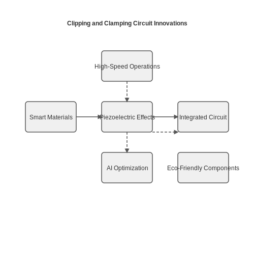
7. Key Textbooks on Electronics
7.1 Key Textbooks on Electronics
For those delving deeply into the nuances of applied clipping and clamping circuits, a comprehensive understanding of electronics as a whole is essential. This encompasses both the fundamental principles and the intricate details that pertain to advanced applications. Below is a curated list of textbooks that cater to advanced-level readers, such as engineers, physicists, researchers, and graduate students. These textbooks not only cover the basics but also provide mathematical rigor and real-world applications, ensuring a holistic understanding of electronics.- The Art of Electronics — Written by Paul Horowitz and Winfield Hill, this book is a cornerstone of electronics literature. It offers in-depth coverage of both analog and digital electronics, with practical insights and updated content in its third edition.
- Electronic Devices and Circuit Theory — Authored by Robert L. Boylestad, this text is renowned for its comprehensive approach to electronic devices and circuit performance. It includes detailed explanations and mathematical formulas essential for any advanced-level reader.
- Microelectronic Circuits — By Adel S. Sedra and Kenneth C. Smith, this book provides a detailed analysis of circuits, encouraging a solid grasp of the principles and their applications in real-life scenarios. It also encompasses appendices on mathematical methods, useful for derivations.
- Analog Integrated Circuit Design — Authored by Tony Chan Carusone, David Johns, and Kenneth Martin, this text offers a sophisticated treatment of analog integrated circuits, focusing on modern design strategies and addressing current technological trends and applications.
- Foundations of Electric Circuits — Reuben Lee takes a methodical approach to the study of electric circuits, integrating both theoretical perspectives and practical applications that are crucial for advanced learners seeking depth in their understanding.
- Electronics and Circuit Analysis Using MATLAB — By John Okyere Attia, this book bridges electronics theory and MATLAB computational skills, useful for real-world applications and simulations, making it invaluable for those interested in applying computational methods alongside theoretical frameworks.
- Introduction to Modern Electronics — J. S. Ragsdale offers a modern take on electronics, emphasizing contemporary technology and providing thorough examples of electronic systems, ideal for those looking to connect foundational knowledge with emerging trends.
7.2 Research Papers and Articles
- Analysis and Synthesis of Clipping and Clamping Circuits — This paper published by IEEE provides an in-depth theoretical and practical analysis of various clipping and clamping circuit designs, offering insights into their essential functions and applications in electronics.
- Study on Clipping Circuits in Power Electronics — This research paper delves into the usage of clipping circuits in power electronic systems, discussing their importance in protecting components from voltage spikes and noise.
- Applications of Clipping and Clamping Techniques in Renewable Energy Systems — This article addresses how clipping and clamping techniques are implemented in renewable energy systems to enhance safety and efficiency, highlighted through various case studies.
- Novel Clamping High Voltage Devices — Offered by IEEE, the paper explores innovative clamping solutions for high voltage devices, emphasizing enhanced protection methods and practical design challenges in modern applications.
- Modern Developments in Clamping Circuit Design — This journal article explains recent advances in clamping circuit designs, focusing on improved techniques for safeguarding integrated circuits from electrical transients.
- Nonlinear Dynamics of Clipping Circuits — Offering a deep dive into the nonlinear behavior of clipping circuits, this paper provides a mathematical study essential for researchers interested in circuit dynamics and modeling.
- Impact of Clamping Technologies on Digital Systems — This article investigates the role of clamping technologies in the evolution of digital systems, emphasizing strategies to mitigate electronic interference in complex circuit architectures.
7.3 Online Resources and Tutorials
- EDN Network: Clipping and Clamping Techniques in Analog Circuits — This article provides a thorough examination of clipping and clamping techniques in analog circuits, focusing on practical application and circuit designs to control signal waveforms.
- All About Circuits: Clamper Circuits — Offers an insightful exploration of various clamper circuits, discussing the theory of operation and typical applications in signal processing.
- Electronics Tutorials: Diode Clamper Circuits — Provides comprehensive tutorials on diode clamping circuits, explaining their function, types, and real-world applications with supportive diagrams.
- Electronics Tutorials: Clippers — This page explores the structure and function of various clipping circuits, offering detailed explanations of how they shape AC waveforms.
- Learn About Electronics: Clipping and Clamping Circuits — Discusses a range of oscillator designs and how clipping and clamping circuits can modify signal amplitude and waveform shapes.
- Circuit Digest: Simple Clipper Circuit — A practical tutorial on building simple clipper circuits, providing schematic diagrams and explanations of their parts and operation.
- Radio-Electronics: Diode Clipping & Clamper Circuits — A detailed guide that explains both clipping and clamping circuits using diodes, complete with analysis of their behavior in signal processing applications.
- Tutorials Point: Clipping Circuits — Offers exhaustive tutorials on clipping circuits, pertaining both theory and practical approaches to implement these into electronic designs.